
AIC1721/1721D
3-pin Low Dropout Linear Regulator
Analog Integrations Corporation
4F, 9, Industry E. 9th Rd, Science Based Industrial Park, Hsinchu Taiwan, ROC
www.analog.com.tw
DS-1721-01
TEL: 886-3-5772500
FAX: 886-3-5772510
1
FEATURES
Low Dropout Voltage of 130mV at 100mA Output
Current (5V Output Version).
Guaranteed 150mA/300mA Output Current.
Internal 1.3
P-MOSFET Draws no Base Current.
Low Ground Current at 55
µA.
1% Accuracy Output Voltage of 3.3V/5V.
Input Voltage Range up to 12V (5V Output
Version).
Extremely Tight Load and Line Regulation.
Fast Transient Response.
Needs only 1
µF for Stability.
Current and Thermal Limiting.
APPLICATIONS
Voltage Regulator for LAN Cards.
Wireless Communication Systems.
Battery Powered Systems.
DESCRIPTION
The AIC1721/1721D is the enhanced CMOS
version of the LP2950. The superior
characteristics of the AIC1721/1721D include
zero base current loss, very low dropout voltage,
and 1% accuracy output voltage. Typica-l ground
current remains approximately 55
µA, from no
load to maximum loading conditions. Dropout
voltage at 100mA output current is significantly
lower than its bipolar counterpart: 130mV for the
AIC1721-5/1721D-5, and 180mV for the
AIC1721/ 1721D. Output current limiting and
thermal limiting are built in to provide maximal
protection to the AIC1721/ 1721D against fault
conditions.
While pin-to-pin compatible with the LP2950 and
the industry industry standard 78XX series of
voltage regulators, the AIC1721/1721D comes in
the popular3-pin SOT-89 or TO-92 packages.
TYPICAL APPLICATION CIRCUIT
+
+
AIC1721/
AIC1721D
10
µF
C
OUT
V
OUT
VOUT
GND
VIN
1
µF
C
IN
V
IN
Negative Voltage Regulator

AIC1721
2
ORDERING INFORMATION
ORDER NUMBER
AIC1721CX
AIC1721-5CX
AIC1721DCX
AIC1721D-5CX
(SOT-89)
AIC1721CZ
AIC1721-5CZ
AIC1721DCZ
AIC1721D-5CZ
(TO-92)
PIN CONFIGURATION
FRONT VIEW
1: VOUT
2: GND
3: VIN
AIC1721X-XXX
1
2
3
1
2
3
PACKAGING TYPE
X: SOT-89
Z: TO-92
TEMPERATURE RANGE
C: 0
∞C~+70∞C
OUTPUT VOLTAGE
DEFAULT: 3.3V
5: 5.0V
OUTPUT CURRENT
DEFAULT: 150mA
D: 300mA
TOP VIEW
1: VOUT
2: GND
3: VIN
ABSOLUTE MAXIMUM RATINGS
Input Supply Voltage ......................................................................................... -0.3~12V
Operating Junction Temperature Range ................................................... -40
∞C~ 125∞C
Storage Temperature Range
................................................................... -65
∞C~150∞C
Power Dissipation
SOT-89 Package ........................... 0. 80W
TO-92
Package ............................. 0.78W
TEST CIRCUIT
Refer to the TYPICAL APPLICATION CIRCUIT

AIC1721
3
ELECTRICAL CHARACTERISTICS
(Ta=25
∞
∞
∞
∞C, C
IN
=1
µ
µ
µ
µF, C
OUT
=10
µ
µ
µ
µF, unless
otherwise specified.)
PARAMETER
TEST CONDITIONS
MIN.
TYP.
MAX.
UNIT
Output Voltage
No Load
AIC1721/1721D-5
AIC1721/1721D
V
IN
=5.5~12V
V
IN
=3.6~12V
4.950
3.267
5.0
3.3
5.050
3.333
V
Output Voltage
Temperature
Coefficiency
(Note 1)
50
150
PPM/
∞C
Line Regulation
I
L
=1mA
AIC1721/1721D-5
AIC1721/1721D
V
IN
=5.5~12V
V
IN
=3.6~12V
3
3
10
10
mV
Load Regulation
(Note 2)
AIC1721-5
AIC1721D-5
AIC1721
AIC1721D
V
IN
=7V, I
L
=0.1~150mA
V
IN
=7V, I
L
=0.1~300mA
V
IN
=5V, I
L
=0.1~150mA
V
IN
=5V, I
L
=0.1~300mA
7
7
7
7
15
25
15
25
mV
Current Limit
(Note 3)
AIC1721-5
AIC1721
AIC1721D-5
AIC1721D
V
IN
=7V, V
OUT
=0V
V
IN
=5V, V
OUT
=0V
V
IN
=7V, V
OUT
=0V
V
IN
=5V, V
OUT
=0V
320
320
320
320
440
440
440
440
mA
Dropout Voltage
(Note 4)
AIC1721/1721D
AIC1721-5
AIC1721
AIC1721D-5
AIC1721D
I
L
=0.1mA
I
L
=150mA
I
L
=150mA
I
L
=300mA
I
L
=300mA
0.2
200
270
400
540
10
300
370
500
640
mV
Ground Current
I
O
=0.1mA~I
MAX
AIC1721/1721D-5
AIC1721/1721D
V
IN
=5.5~12V
V
IN
=4~12V
55
55
80
80
µA
Note 1:
Guaranteed by design.
Note 2:
Regulation is measured at constant junction temperature, using pulse testing with a low ON time.
Note 3:
Current limit is measured by pulsing a short time.
Note 4:
Dropout voltage is defined as the input to output differential at which the output voltage drops
100mV below the value measured with a 1V differential.
AIC1721
4
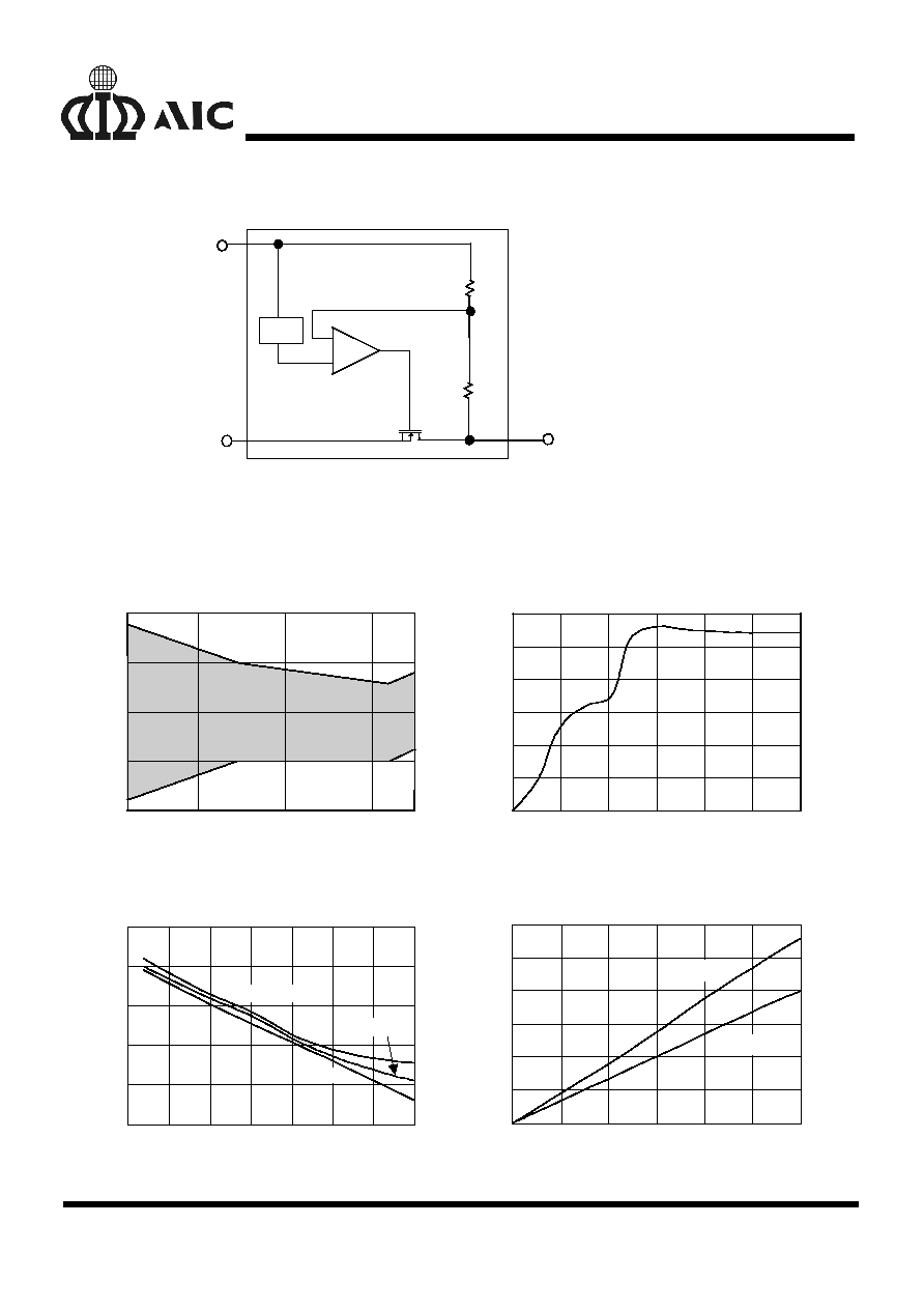
BLOCK DIAGRAM
+
VOUT
VIN
GND
-
+
-
V
REF
TYPICAL PERFORMANCE CHARACTERISTICS
Output Voltage vs. Temperature
Nor
m
ali
z
e
d
O
u
t
p
ut
Vo
l
t
a
g
e
(
%
)
Temperature (
∞C)
0
50
100
98
99
100
101
102
0
-40
125
Ground Current vs. Input Voltage
G
r
ou
nd Cu
r
r
ent
(µ
A)
Input Voltage (V)
0
10
20
30
40
50
60
0
2
4
6
8
10
12
Ground Current vs. Temperature
G
r
o
u
n
d
C
u
r
r
e
n
t (
µ
A)
Temperature(
∞C)
125
0
25
50
75
100
-25
-50
50
52
54
56
58
60
I
L
=0.1mA
I
L
=150mA
I
L
=300mA
Dropout Voltage vs Load Current
Dr
opout
V
o
lta
ge (
m
V
)
Load Current (mA)
600
0
50
100
150
200
250
300
0
100
200
300
400
500
V
OUT
=3.3V
V
OUT
=5V

AIC1721
5
TYPICAL PERFORMANCE CHARACTERISTICS
(Continued)
Temperature(∞C)
Dropout Voltage vs Temperature
D
r
o
p
ou
t
V
o
l
t
ag
e
(
m
V
)
0
25
50
75
100
125
-25
-50
0
100
200
300
400
500
600
I
L
=0.1mA
V
OUT
=5V
I
L
=150mA
I
L
=300mA
Temperature (
∞C)
Short Circuit Current vs. Temperature
S
h
or
t Ci
r
c
ui
t C
u
r
r
e
n
t (
m
A
)
0
25
50
75
100
125
-25
-50
200
300
400
500
AIC1721D
AIC1721
Line Transient Response
Time (mS)
I
n
pu
t
V
o
l
t
ag
e
(V
)
O
u
t
put
V
o
l
t
ag
e
(
m
V,
AC
)
0
0.1
0.2
0.3
0.4
0.5
0.6
0.7
0.8
0.9
1.0
100
50
0
-50
8
6
C
OUT
=1µF
I
L
=1mA
V
OUT
=5V
Load Transient Response
Time (mS)
Load C
u
r
r
en
t
(
m
A)
O
u
t
p
u
t
V
o
l
t
a
g
e
(
m
V
)
150
0.1
100
0
-100
-200
0
0.5
1.0
1.5
2.0
2.5
3.0
3.5
4.0
4.5
5.0
C
OUT
=1
µF
V
OUT
=5V
Load Transient Response
Time (mS)
L
oad C
u
r
r
ent
(m
A
)
O
u
t
put
V
o
l
t
age
(
m
V,
AC
)
0
0.5
1.0
1.5
2.0
2.5
3.0
3.5
4.0
4.5
5.0
20
0
-20
150
0.1
C
OUT
=10
µF
V
OUT
=5V
-40
-60