
AIC1721/1721D
150mA/300mA Low Dropout Linear Regulator
with 1% Output Accuracy
Analog Integrations Corporation
4F, 9 Industry E. 9th Rd, Science-Based Industrial Park, Hsinchu, Taiwan
DS-1721-01 032502
TEL: 886-3-5772500
FAX: 886-3-5772510
www.analog.com.tw
1
n
FEATURES
l
Low Dropout Voltage of 130mV at 100mA Output
Current (5V Output Version).
l
Guaranteed 150mA/300mA Output Current.
l
Internal 1.3
P-MOSFET Draws no Base Current.
l
Low Ground Current: 55
µ
A.
l
1% Accuracy Output Voltage of 3.3V/5V.
l
Input Voltage Range up to 12V (5V Output
Version).
l
Extremely Tight Load and Line Regulation.
l
Fast Transient Response.
l
Needs only 1
µ
F Output Capacitor for Stability.
l
Current Limiting and Thermal Protection.
n
APPLICATIONS
l
Voltage Regulator for LAN Cards.
l
Wireless Communication Systems.
l
Battery Powered Systems.
n
DESCRIPTION
The AIC1721/1721D is the enhanced CMOS
version of the LP2950. The superior
characteristics of the AIC1721/1721D include
zero-base current loss, very low dropout voltage,
and 1% accuracy output voltage. Typical ground
current remains approximately 55
µ
A, under the
output condition of from zero up to the maximum
Load. Dropout voltage at 100mA output current is
significantly lower than its bipolar counterpart:
130mV for the AIC1721-50/1721D-50, and
180mV for the AIC1721/ 1721D. Output current
limiting and thermal protections are built to
protect AIC1721/1721D against fault condition.
AIC1721 and AIC1721D come with SOT-89 and
TO-92 packages of 3-pins, whose definitions are
the same as those of LP2950 and standard 78XX.
n
TYPICAL APPLICATION CIRCUIT
+
+
AIC1721/
AIC1721D
10
µ
F
C
OUT
V
OUT
VOUT
GND
VIN
1
µ
F
C
IN
V
IN
Low Dropout Linear Regulator

AIC1721/1721D
2
n
ORDERING INFORMATION
PACKING TYPE
TR: TAPE & REEL
BG: BAG
PACKAGE TYPE
X: SOT-89
Z: TO-92
OUTPUT VOLTAGE
DEFAULT: 3.3V
50: 5.0V
OUTPUT CURRENT
DEFAULT: 150mA
D: 300mA
AIC1721X-XXCXXX
Example: AIC1721CXTR
ý
150mA, 3.3V Version, in SOT-89
Package & Tape & Reel Packing Type
SOT-89
FRONT VIEW
1. VOUT
2. GND
3. VIN
1
2
3
1
2
3
PIN CONFIGURATION
TO-92
FRONT VIEW
1. GND
2. VIN
3.
VOUT
n
ABSOLUTE MAXIMUM RATINGS
Input Supply Voltage .................................... ... ... ... ......... ... ................................ -0.3~12V
Operating Junction Temperature Range ................. ........ ... ..... .... .............. -40
∞
C~ 125
∞
C
Storage Temperature Range
................................. .... ... ... ........................ -65
∞
C~150
∞
C
Power Dissipation
SOT-89 Package ..... .... ... .... ........... 0. 80W
TO-92 Package .......... ... .... ............ 0.78W
n
TEST CIRCUIT
Refer to the TYPICAL APPLICATION CIRCUIT

AIC1721/1721D
3
n
ELECTRICAL CHARACTERISTICS
(T
J
=25
∞
C, C
IN
=1
µ
F, C
OUT
=10
µ
F, unless
otherwise specified.)
PARAMETER
TEST CONDITIONS
MIN.
TYP.
MAX.
UNIT
Output Voltage
AIC1721/1721D-50
AIC1721/1721D
V
IN
=5.5~12V, I
OUT
=0mA
V
IN
=3.6~12V, I
OUT
=0mA
4.950
3.267
5.0
3.3
5.050
3.333
V
Output Voltage
Temperature
Coefficiency
(Note 1)
50
150
PPM/
∞
C
Line Regulation
I
OUT
=1mA
AIC1721/1721D-50
AIC1721/1721D
V
IN
=5.5~12V
V
IN
=3.6~12V
3
3
10
10
mV
Load Regulation
(Note 2)
AIC1721-50
AIC1721D-50
AIC1721
AIC1721D
V
IN
=7V, I
OUT
=0.1~150mA
V
IN
=7V, I
OUT
=0.1~300mA
V
IN
=5V, I
OUT
=0.1~150mA
V
IN
=5V, I
OUT
=0.1~300mA
7
7
7
7
15
25
15
25
mV
Current Limit
(Note 3)
AIC1721-50
AIC1721
AIC1721D-50
AIC1721D
V
IN
=7V, V
OUT
=0V
V
IN
=5V, V
OUT
=0V
V
IN
=7V, V
OUT
=0V
V
IN
=5V, V
OUT
=0V
300
300
300
300
440
440
440
440
mA
Dropout Voltage
(Note 4)
AIC1721-50
AIC1721
AIC1721D-50
AIC1721D
I
OUT
=150mA
I
OUT
=150mA
I
OUT
=300mA
I
OUT
=300mA
200
270
400
540
300
370
500
640
mV
Ground Current
I
OUT
=0.1mA~I
MAX
AIC1721/1721D-50
AIC1721/1721D
V
IN
=5.5~12V
V
IN
=4~12V
55
55
80
80
µ
A
Note 1:
Guaranteed by design.
Note 2:
Regulation is measured at constant junction temperature, using pulse testing with a low ON time.
Note 3:
Current limit is measured by pulsing a short time.
Note 4:
Dropout voltage is defined as the input to output differential at which the output voltage drops
100mV below the value measured with a 1V differential.
AIC1721/1721D
4
n
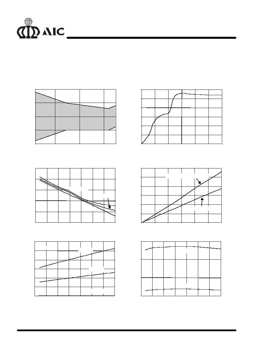
TYPICAL PERFORMANCE CHARACTERISTICS
Fig. 1 Output Voltage vs. Temperature
Normalized Output
Voltage (%)
Temperature (
∞
C)
0
50
100
96
98
100
103
104
0
-40
125
Fig. 2 Ground Current vs. Input Voltage
G
round Current (
µ
A)
Input Voltage (V)
0
10
20
30
40
50
60
0
2
4
6
8
10
12
Fig. 3 Ground Current vs. Temperature
Ground Current (
µ
A)
Temperature (
∞
C)
125
0
25
50
75
100
-25
-50
50
52
54
56
58
60
I
L
=300mA
I
L
=150mA
I
L
=0.1mA
Fig. 4 Dropout Voltage vs. Load Current
Dropout Voltage (mV)
Load Current (mA)
600
0
50
1 00
150
2 00
2 50
3 00
0
100
200
300
400
500
V
OUT
=5.0V & 5.2V
V
OUT
=3.3V, 3.5V, 3.7V & 3.8V
Temperature(
∞
C)
Fig. 5 Dropout Voltage vs Temperature
Dropout
Voltage(mV)
0
25
50
75
100
125
-25
-50
0
100
200
300
400
500
600
I
L
=0.1mA
V
OUT
=5V
I
L
=150mA
I
L
=300mA
Temperature (
∞
C)
Fig. 6 Short Circuit Current vs. Temperature
Short Circuit Current (
mA)
0
25
50
75
100
125
-25
-50
200
300
400
500
AIC1721D
AIC1721

AIC1721/1721D
5
n
TYPICAL PERFORMANCE CHARACTERISTICS
(Continued)
Fig. 7 Line Transient Response
Time (mS)
Input Voltage
(V)
Output Voltage
(
mV, AC)
0
0.1
0.2
0.3
0.4
0.5
0.6
0.7
0.8
0.9
1.0
100
50
0
-50
8
6
C
OUT
=1
µ
F
I
L
=1mA
V
OUT
=5V
Fig. 8 Load Transient Response
Time (mS)
Load Current
(
mA)
Output Voltage
(
mV, AC)
150
0.1
100
0
-100
-200
0
0.5
1.0
1.5
2.0
2.5
3.0
3.5
4.0
4.5
5.0
C
OUT
=1
µ
F
V
OUT
=5V
Fig. 9 Load Transient Response
Time (mS)
Load Current
(
mA)
Output Voltage
(
mA, AC)
0
0.5
1.0
1.5
2.0
2.5
3.0
3.5
4.0
4.5
5.0
20
0
-20
150
0.1
C
OUT
=10
µ
F
V
OUT
=5V
-40
-60
n
BLOCK DIAGRAM
V
REF
1.235V
GND
VOUT
VIN
ERROR
AMP
+
-
THERMAL
LIMITING
-
+
CURRENT
LIMITING