AIC1733
500mA, Low Dropout Linear Regulator with Shutdown
Analog Integrations Corporation
Si-Soft Research Center
DS-1733P-03 092304
3A1, No.1, Li-Hsin Rd. I , Science Park , Hsinchu 300, Taiwan , R.O.C.
TEL: 886-3-5772500
FAX: 886-3-5772510
www.analog.com.tw
1
FEATURES
Active Low Shutdown Control.
Very Low Quiescent Current.
Very Low Dropout Voltage of 650mV at 500mA
Output Current (3.0V Output Version)
1.5V, 1.8V, 2.5V, 2.8V, 3.0V, 3.3V Output Voltage.
Short Circuit and Thermal Protection.
±2% Output Tolerance.
Miniature Package: SOT-23-5
APPLICATIONS
PDA
DSC
Notebook
Pagers
Personal Communication Equipment
Cordless Telephones
Portable Instrumentation
Portable Consumer Equipment
Battery Powered Systems
DESCRIPTION
AIC1733 is a 500mA low noise, low dropout
linear regulator, and is housed in small SOT-23-5
package. The device is in the "ON" state when
the SHDN pin is set to logic high level. An
internal P-MOSFET pass transistor is used to
achieve 650mV low dropout voltage at 500mA
load current. It offers high precision output
voltage of
±2%. The quality of low quiescent
current and low dropout voltage makes this
device ideal for battery power applications. The
internal reverse bias protection eliminates the
requirement for a reverse voltage protection
diode. The high ripple rejection and low noise of
AIC1733 provide enhanced performance for
critical applications. The noise bypass pin can be
connected an external capacitor to reduce the
output noise level.
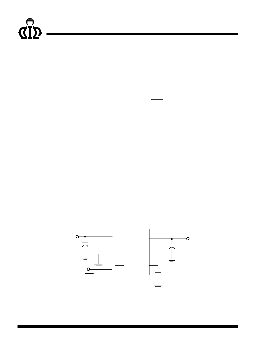
TYPICAL APPLICATION CIRCUIT
C
IN
1
µF
V
IN
BP
VOUT
SHDN
GND
VIN
AIC1733
C
OUT
1
µF
C
BP
0.1
µF
V
SHDN
V
OUT
+
+
Low Noise Low Dropout Linear Regulator
AIC1733
ORDERING INFORMATION
PACKING TYPE
TR: TAPE & REEL
BG: BAG
PACKAGE TYPE
V: SOT-23-5
C: COMMERCIAL
P: LEAD FREE COMMERCIAL
OUTPUT VOLTAGE
15:
1.5V
18:
1.8V
25:
2.5V
28:
2.8V
30:
3.0V
33:
3.3V
AIC1733-XXXXXX
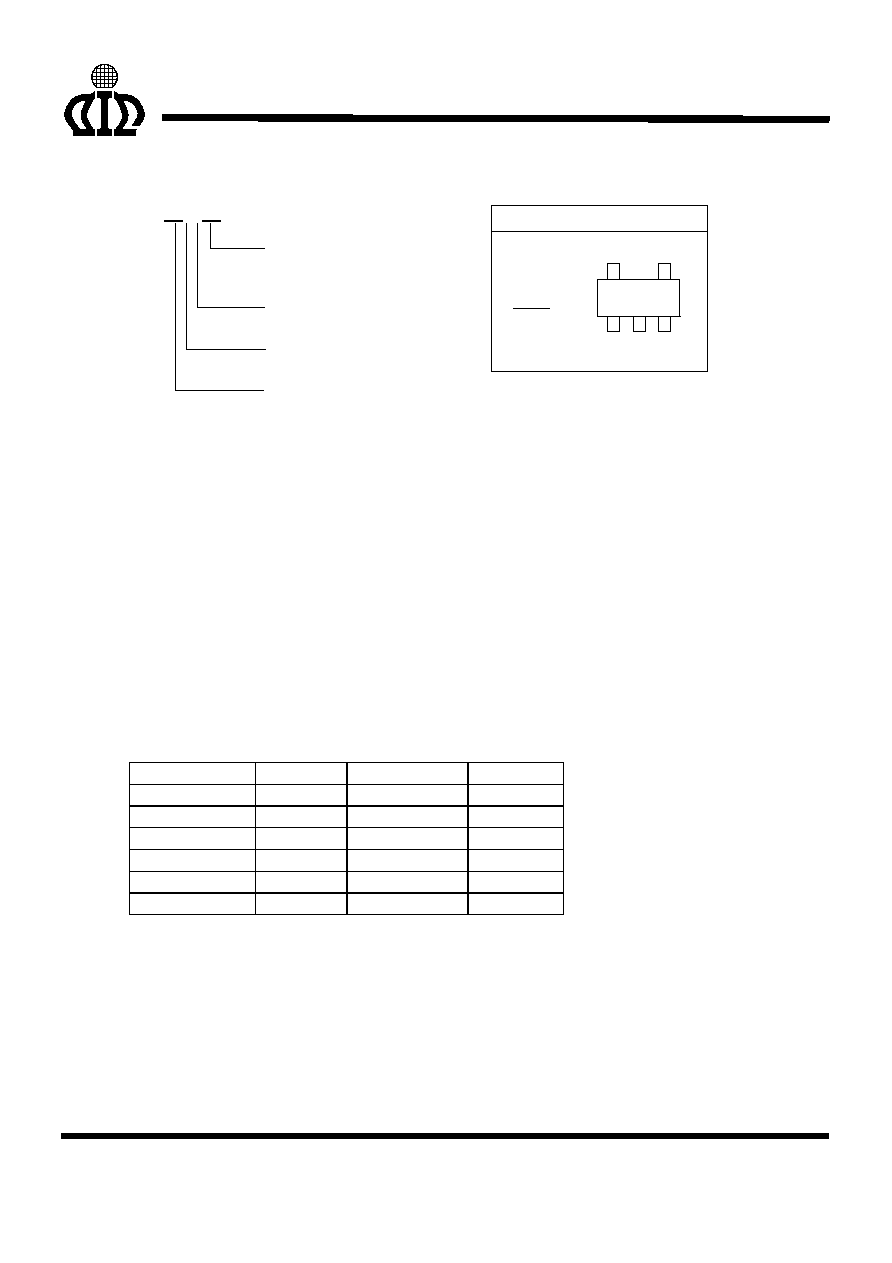
PIN CONFIGURATION
SOT-23-5 (CV)
TOP VIEW
1: VIN
2: GND
3: SHDN
4: BP
5: VOUT
3
2
1
4
5
(Of a unit of 0.1V within the voltage range from 1.5V to 3.3V, additional
voltage versions for this product line may be available on demand with
prior consultation with AIC.)
Example: AIC1733-18CVTR
1.8V Version, in SOT-23-5 Package & Tape & Reel
Packing Type
AIC1733-18PVTR
1.8V Version, in SOT-23-5 Lead Free Package & Tape &
Reel Packing Type
∑
SOT-23-5 Marking
Part No.
Marking
Part No.
Marking
AIC1733-15CV EE15 AIC1733-15PV
EE15P
AIC1733-18CV EE18 AIC1733-18PV
EE18P
AIC1733-25CV EE25 AIC1733-25PV
EE25P
AIC1733-28CV EE28 AIC1733-28PV
EE28P
AIC1733-30CV EE30 AIC1733-30PV
EE30P
AIC1733-33CV EE33 AIC1733-33PV
EE33P
2
AIC1733
ABSOLUTE MAXIMUM RATINGS
Supply Voltage
................................................................................................12V
Shutdown Terminal Voltage ...............................................................................12V
Noise Bypass Terminal Voltage
............................................................................5V
Operating Temperature Range
...............................................................-40∫C~85∫C
Maximum Junction Temperature
125
∞C
Storage Temperature Range
...................................................................-65∫C~150∫C
Lead Temperature (Soldering, 10 sec)
260
∞C
Thermal Resistance (Junction to Case) SOT-23-5
........................................130
∞C /W
Thermal Resistance Junction to Ambient SOT-23-5 ........................................220
∞C /W
(Assume no ambient airflow, no heatsink)
Absolute Maximum Ratings are those values beyond which the life of a device may be impaired.
TEST CIRCUIT
Refer to TYPICAL APPLICATION CIRCUIT.
3
AIC1733
ELECTRICAL CHARACTERISTICS
(C
IN
=1
µF, C
OUT
=4.7
µF, T
J
=25
∞C, unless otherwise specified)
PARAMETER
TEST CONDITIONS
SYMBOL MIN. TYP. MAX.
UNIT
Quiescent Current
I
OUT
= 0mA, V
IN
= 3.6~7V
I
Q
40
55
µA
Standby Current
V
IN
= 3.6~7V, output OFF
I
STBY
0.1
µA
GND Pin Current
I
OUT
= 0.1~500mA
I
GND
30
50
µA
Continuous Output Current
V
IN
= 5V
I
OUT
500
mA
Output Current Limit
V
IN
= 5V, V
OUT
= 0V
I
IL
500 600
mA
Output Voltage Tolerance
V
IN
= 5V, no load
V
OUT
-2 2 %
Temperature Coefficient
TC
50
150
ppm/∫C
Line Regulation
V
IN
= V
OUT(TYP)
+ 1V to 7V
V
LIR
3 10 mV
Load Regulation
V
IN
= V
OUT
+ 1.2V (Vout 2.5V)
V
IN
= V
OUT
+ 1.8V (Vout 2.4V)
I
OUT
= 0.1~500mA
V
LOR
20 40 mV
Dropout Voltage
I
L
=500mA
3.0V
V
OUT
3.3V
2.5V
V
OUT
2.9V
2.0V
V
OUT
2.4V
1.5V
V
OUT
1.9V
V
DROP
650
780
1100
1400
1050
1180
1500
1800
mV
Noise Bypass Terminal Voltage
V
REF
1.23
V
Output Noise
C
BP
= 0.1
µF, f = 1KHz,V
IN
= 5V
n
0.46
Hz
V
µ
Ripple Rejection
f = 1KHz, Ripple = 0.5V
P-P
,
C
BP
= 0.1
µF
RR 55 dB
4
AIC1733
ELECTRICAL CHARACTERISTICS
(Continued)
PARAMETER
TEST CONDITIONS
SYMBOL MIN. TYP. MAX.
UNIT
SHUTDOWN TERMINAL SPECIFICATIONS
Shutdown Pin Current
I
SHDN
0.1
µA
Shutdown Pin Voltage (ON)
Output ON
V
SHDN
(ON)
1.6 V
Shutdown Pin Voltage (OFF)
Output OFF
V
SHDN
(OFF)
0.6 V
Shutdown Exit Delay Time
C
BP
= 0.1
µF, C
OUT
= 1
µF,
I
OUT
=30mA
t 300 µS
THERMAL PROTECTION
Thermal Shutdown Temperature
T
SD
155 ∫C
Note 1: Specifications are production tested at TA=25
∞C. Specifications over the -40∞C to 85∞C operating
temperature range are assured by design, characterization and correlation with Statistical Quality
Controls (SQC).
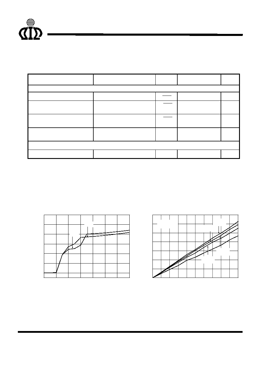
TYPICAL PERFORMANCE CHARACTERISTICS
0
1
2
3
4
5
6
7
0
10
20
30
40
50
60
Fig. 1 Quiescent Current vs. V
IN
3.3V
1.5V
Q
u
iesc
ent current
(
µ
A
)
V
IN
(V)
Fig. 2 V
DROP
vs. I
LOAD
V
DR
O
P
(mV)
I
LOAD
(V)
0
50
100
150
200
250
300
350
400
450
500
0
100
200
300
400
500
600
700
AIC1733-33
T=50
∞C
T=80
∞C
T=-40
∞C
T=200
∞C
5
AIC1733
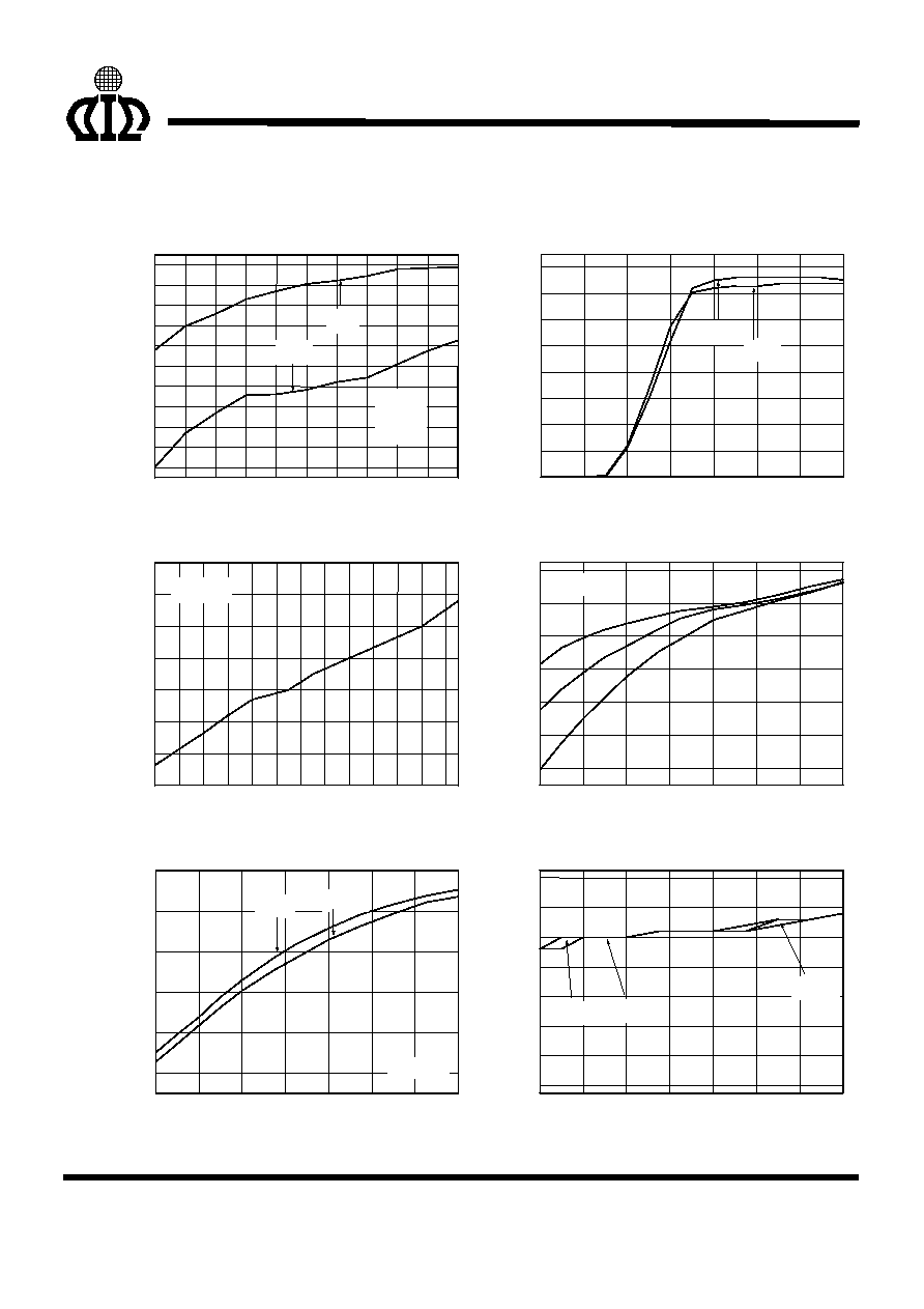
TYPICAL PERFORMANCE CHARACTERISTICS
(Continued)
Fig. 3 Ground Current vs. I
LOAD
Grou
nd C
u
rren
t
(
µ
A)
I
LOAD
(V)
0
50
100
150
200
250
300
350
400
450
500
39.0
39.5
40.0
40.5
41.0
41.5
42.0
42.5
43.0
43.5
44.0
V
IN
=5V
T=25
∞C
3.3V
1.5V
Fig. 4 Input Voltage vs. Short Circuit Current
Sh
ort C
i
r
c
uit C
u
r
r
en
t
(m
A)
Input Voltage(V)
0
1
2
3
4
5
6
7
0
100
200
300
400
500
600
700
800
1.5V
3.3V
Fig. 5 V
DROP
vs. Temperature
V
DROP
(V)
Temperature (
∞C)
-40
-30
-20
-10
0
10
20
30
40
50
60
70
80
1.36
1.38
1.40
1.42
1.44
1.46
1.48
1.50
AIC1733-15
Fig. 6 Ground Current vs. Temperature
Grou
nd C
u
rren
t
(
µ
A)
Temperature (
∞C)
-40
-20
0
20
40
60
80
100
39
40
41
42
43
44
45
AIC1733-33
150mA
300mA
500mA
Fig. 7 Quiescent
vs. Temperature
Qui
e
sce
nt Curren
t (V)
Temperature (
∞C)
-40
-20
0
20
40
60
80
100
36
38
40
42
44
46
V
IN
=
5V
3.3V
1.5V
Fig. 8 Current Limit vs. Temperature
Current Limi
t
(m
A
)
Temperature (
∞C)
-40
-20
0
20
40
60
80
100
560
600
640
680
720
760
800
840
V
IN
=7V
V
IN
=6V
V
IN
=5V
6
AIC1733
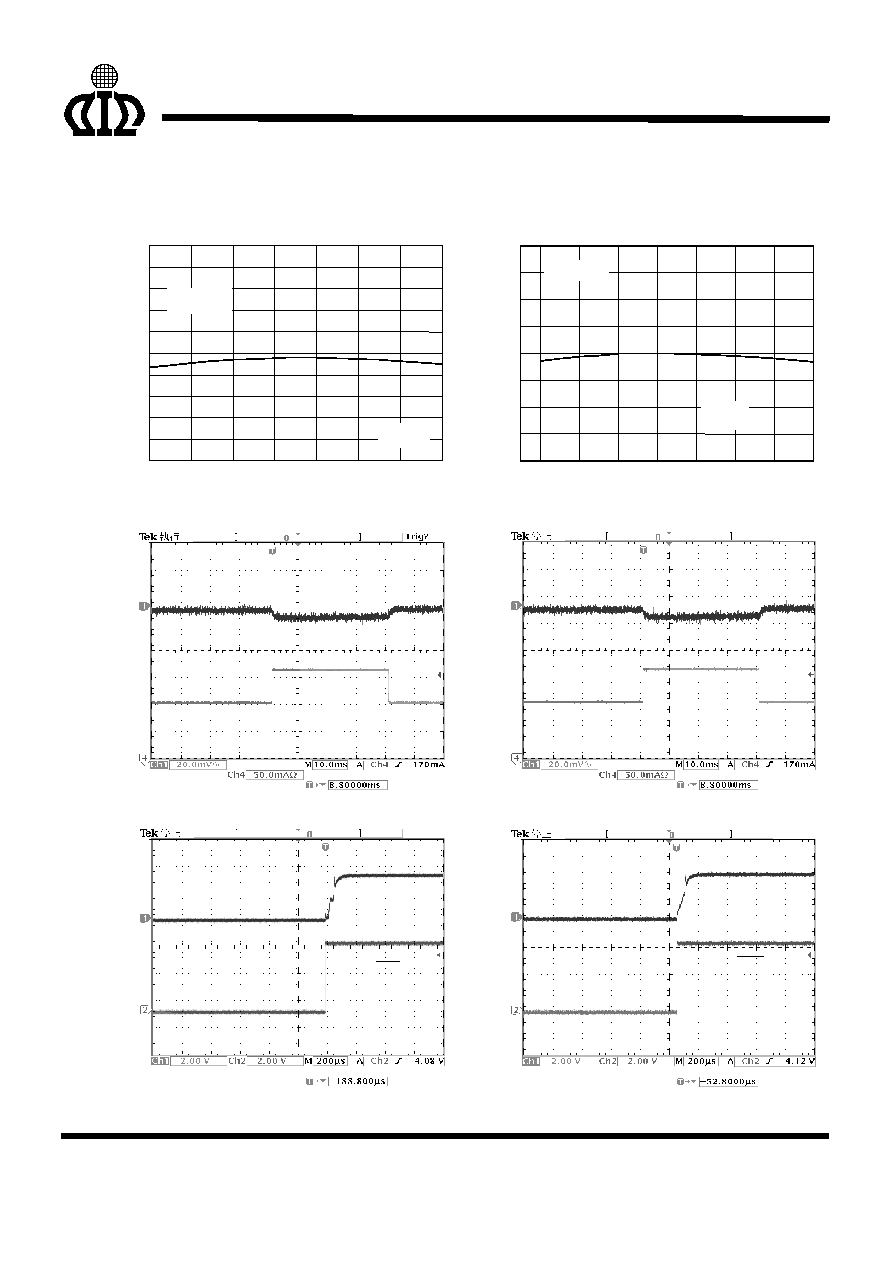
TYPICAL PERFORMANCE CHARACTERISTICS
(Continued)
Fig. 9 V
OUT
vs. Temperature
Out
put V
o
lt
age
(V)
Temperature (
∞C)
-40
-20
0
20
40
60
80
100
1.40
1.42
1.44
1.46
1.48
1.50
1.52
1.54
1.56
1.58
1.60
V
IN
=
5V
AIC1733-15
Fig. 10 V
OUT
vs. Temperature
Out
put V
o
lt
age
(V)
Temperature (
∞C)
-40
-20
0
20
40
60
80
100
3.10
3.15
3.20
3.25
3.30
3.35
3.40
3.45
3.50
V
IN
=5V
AIC1733-33
Fig. 11 Load Transient Response
C
OUT
=4.7
µF
C
BP
=0.1
µF
I
OUT
=120mA
I
OUT
=180mA
V
OUT
Fig. 12 Load Transient Response
C
OUT
=1
µF
C
BP
=0.1
µF
I
OUT
=120mA
I
OUT
=180mA
V
OUT
Fig. 13 Shutdown Exit Time
I
OUT
=30mA
C
BP
=0.1
µF,C
OUT
=1
µF
V
SHDN
V
OUT
Fig. 14 Shutdown Exit Time
I
OUT
=30mA
C
BP
=0.1
µF
C
OUT
=4.7
µF
V
SHDN
V
OUT
7
AIC1733
TYPICAL PERFORMANCE CHARACTERISTICS
(Continued)
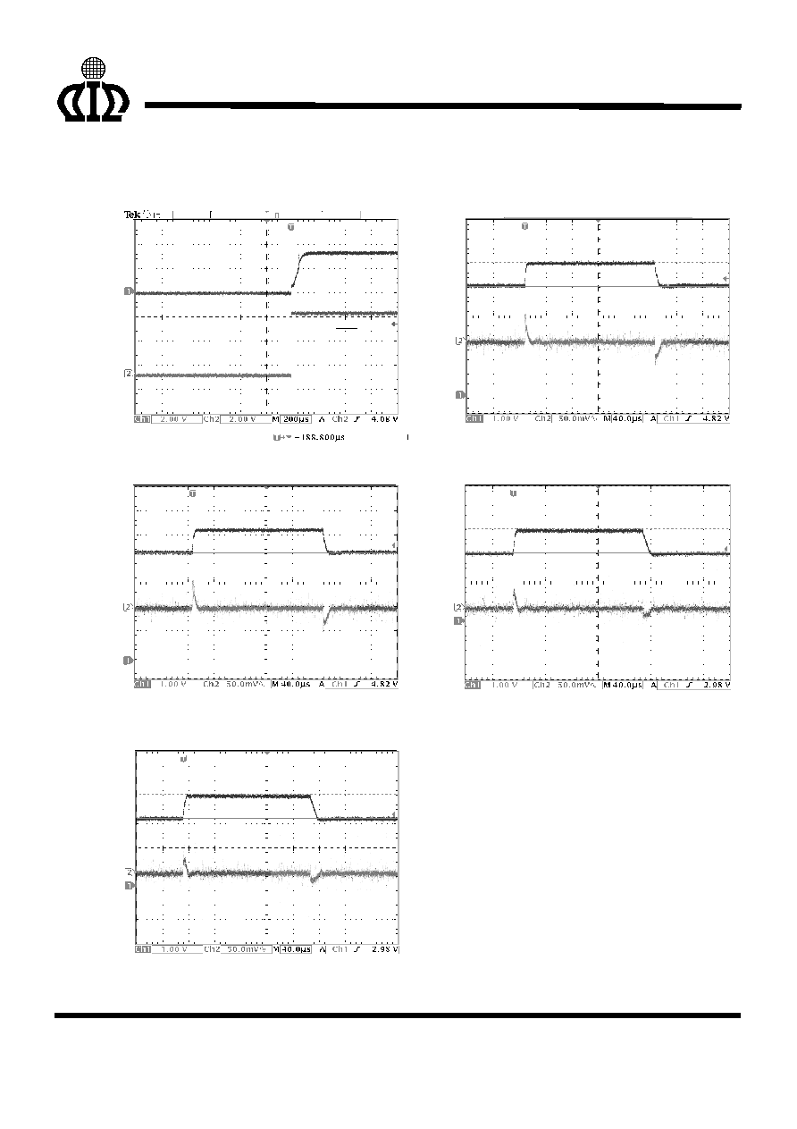
Fig. 15 Shutdown Exit Time
I
OUT
=30mA
C
BP
=0.1
µF,C
OUT
=10
µF
V
SHDN
V
OUT
Fig. 16 Line Transient Response
V
OUT
=3.3V
C
IN
=1
µF, C
OUT
=1
µF
C
BP
=0.1
µF
Iout=50mA
Vin=V
OUT
+1V
Vin=V
OUT
+2V
Fig. 17 Line Transient Response
V
OUT
=3.3V
C
IN
=1
µF, C
OUT
=4.7
µF
C
BP
=0.1
µF
Iout=50mA
Vin=V
OUT
+1V
Vin=V
OUT
+2V
Fig. 18 Line Transient Response
V
OUT
=1.5V
C
IN
=1
µF, C
OUT
=1
µF
C
BP
=0.1
µF
Iout=50mA
Vin=V
OUT
+1V
Vin=V
OUT
+2V
Fig. 19 Line Transient Response
V
OUT
=1.5V
C
IN
=1
µF, C
OUT
=4.7
µF
C
BP
=0.1
µF
IIout=50mA
Vin=V
OUT
+1V
Vin=V
OUT
+2V
8
AIC1733
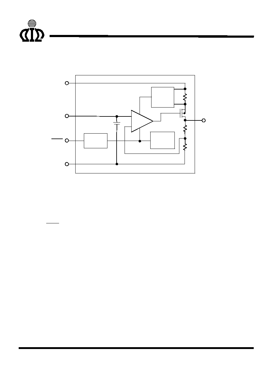
BLOCK DIAGRAM
Current
Limiting
Error
Amp.
-
+
Thermal
Limiting
VOUT
Power
Shutdown
BP
VIN
V
REF
1.23V
GND
SHDN
PIN DESCRIPTIONS
PIN 1 : VIN - Power supply input pin. Bypass
with a 1
µF capacitor to GND
PIN 2 : GND - Ground pin.
PIN 3 :
SHDN
- Active-Low shutdown input pin.
PIN 4 : BP - Noise bypass pin. An external
bypass capacitor connected to
BP pin reduces noises at the
output.
PIN 5 : VOUT - Output pin. Sources up to 500
mA.
DETAILED DESCRIPTIONS OF TECHNICAL TERMS
DROPOUT VOLTAGE (V
DROP
)
The dropout voltage is defined as the difference
between the input voltage and output voltage at
which the output voltage drops 100mV. Below
this value, the output voltage will fall as the input
voltage reduces. It depends on the load current
and junction temperature.
LINE REGULATION
Line regulation is the ability of the regulator to
maintain a constant output voltage as the input
voltage changes. The line regulation is specified
as the input voltage changes from V
IN
= V
OUT
+
1V to V
IN
= 7V and I
OUT
= 1mA.
LOAD REGULATION
Load regulation is the ability of the regulator to
maintain a constant output voltage as the load
current changes.
A pulsed measurement with an
input voltage set to V
IN
= V
OUT
+ V
DROP
can
minimize temperature effects.
The load regulation
is specified by the output current ranging from
0.1mA to 500mA.
9
AIC1733
CURRENT LIMIT (I
IL
)
AIC1733 includes a current limiting, which
monitors and controls the maximum output
current if the output is shorted to ground. This
can protect the device from being damaged.
THERMAL PROTECTION
Thermal sensor protects device when the
junction temperature exceeds T
J
= +155∫C. It
signals shutdown logic, turning off pass transistor
and allowing IC to cool down. After the IC's
junction temperature cools by 15∫C, the thermal
sensor will turn the pass transistor back on.
Thermal protection is designed to protect the
device in the event of fault conditions. For a
continuous operation, do not exceed the absolute
maximum junction-temperature rating of T
J
=
150∫C, or damage may occur to the device.
APPLICATION INFORMATION
INPUT-OUTPUT CAPACITORS
Linear regulators require input and output
capacitors to maintain stability. Input capacitor at
1
µF with a 4.7uF aluminum electrolytic output
capacitor is recommended. To avoid oscillation,
ceramic capacitor is rejected.
NOISE BYPASS CAPACITOR
0.1
µF bypass capacitor at BP pin reduces output
voltage noise. And the BP pin has to connect a
capacitor to GND.
POWER DISSIPATION
The maximum power dissipation of AIC1733
depends on the thermal resistance of its case
and circuit board, the temperature difference
between the die junction and ambient air, and
the rate of airflow. The rate of temperature rise is
greatly affected by the mounting pad
configuration on the PCB, the board material,
and the ambient temperature. When the IC
mounting with good thermal conductivity is used,
the junction temperature will be low even when
large power dissipation applies.
The power dissipation across the device is
P = I
OUT
(V
IN
-V
OUT
).
The maximum power dissipation is:
)
R
(R
)
T
(T
P
BA
JB
A
J
MAX
+
-
=
Where T
J
-T
A
is the temperature difference
between the die junction and the surrounding air,
R
JB
is the thermal resistance of the package,
and R
BA
is the thermal resistance through the
PCB, copper traces, and other materials to the
surrounding air.
As a general rule, the lower temperature is, the
better reliability of the device is. So the PCB
mounting pad should provide maximum thermal
conductivity to maintain low device temperature.
GND pin performs a dual function of providing
an electrical connection to ground and
channeling heat away. Therefore, connecting
the GND pin to ground with a large pad or
ground plane would increase the power
dissipation and reduce the device temperature
10
AIC1733
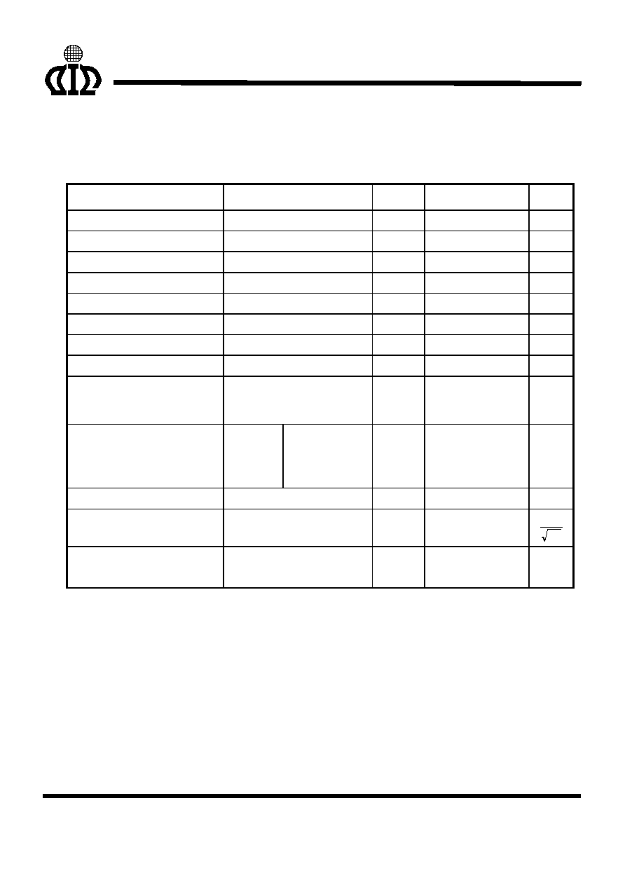
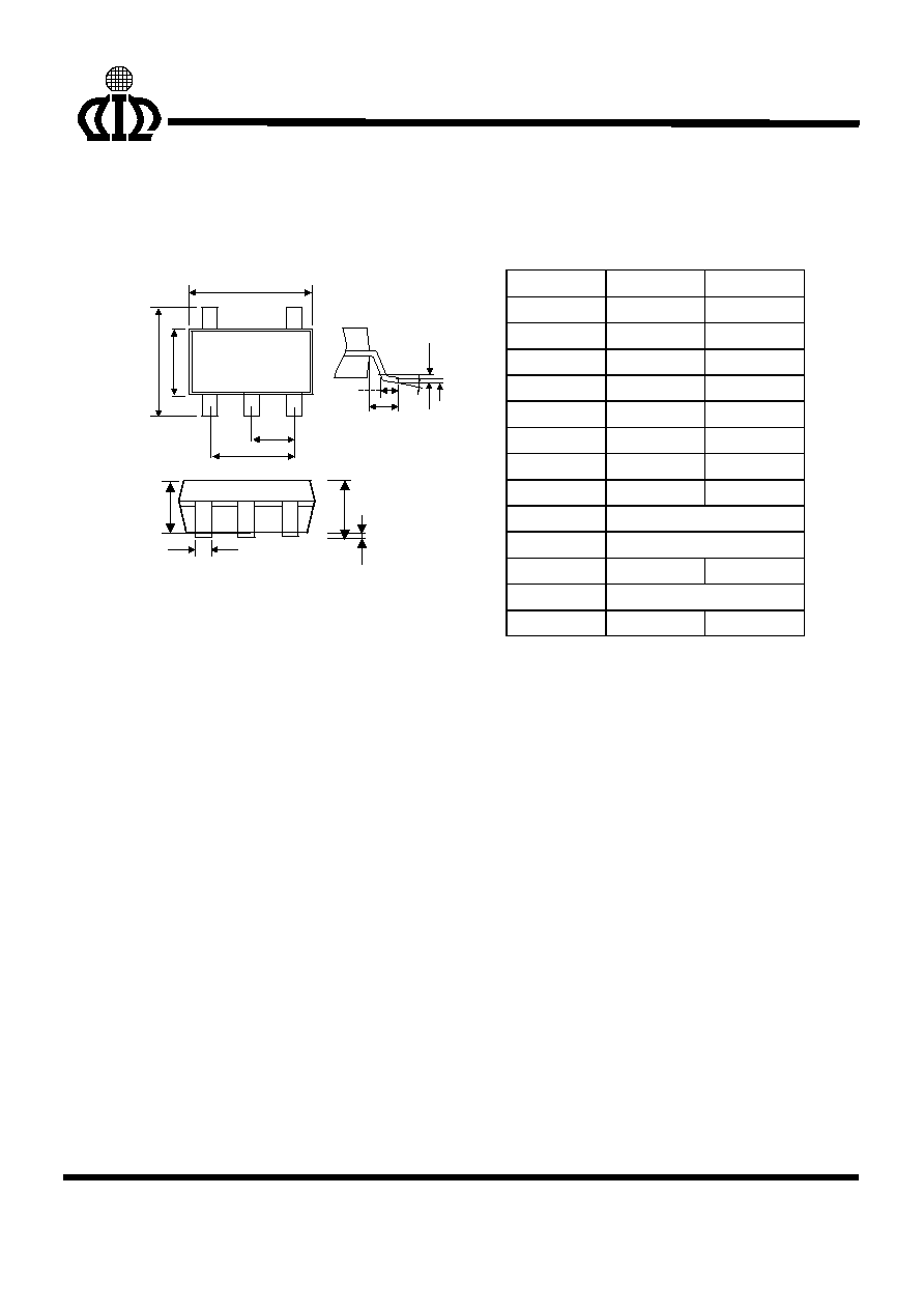
PHYSICAL DIMENSIONS
SOT-23-5 (unit: mm)
SYMBOL MIN MAX
A 0.95
1.45
A1 0.05 0.15
A2 0.90 1.30
b 0.30
0.50
c 0.08
0.22
D 2.80
3.00
E 2.60
3.00
E1 1.50 1.70
e 0.95
BSC
e1 1.90
BSC
L 0.30
0.60
L1 0.60
REF
E1
e1
D
E
e
A1
A
A2
b
0.25
L1
L
c
0
∞
8
∞
Note:
Information provided by AIC is believed to be accurate and reliable. However, we cannot assume responsibility for use of any
circuitry other than circuitry entirely embodied in an AIC product; nor for any infringement of patents or other rights of third parties
that may result from its use. We reserve the right to change the circuitry and specifications without notice.
Life Support Policy: AIC does not authorize any AIC product for use in life support devices and/or systems. Life support devices or
systems are devices or systems which, (I) are intended for surgical implant into the body or (ii) support or sustain life, and whose
failure to perform, when properly used in accordance with instructions for use provided in the labeling, can be reasonably
expected to result in a significant injury to the user.
11