
AIC1803
Three-Cell Lithium-Ion Battery Protection IC
Analog Integrations Corporation
4F, 9 Industry E. 9th Rd, Science-Based Industrial Park, Hsinchu, Taiwan
DS-1803-02 012102
TEL: 886-3-5772500
FAX: 886-3-5772510
www.analog.com.tw
1
n
FEATURES
l
Ultra-Low Quiescent Current at 13
µ
A (V
CELL
=3.5V).
l
Ultra-Low Power-Down Current at 1.3
µ
A (V
CELL
=2.3V)
l
Wide Supply Voltage Range: 2V to 18V.
l
Precision Overcharge Protection Voltage:
4.35V
±
30mV for the AIC1803A
4.30V
±
30mV for the AIC1803B
4.25V
±
30mV for the AIC1803C
4.20V
±
30mV for the AIC1803D
l
Externally Set Overcharge,
Overdischarge and
Overcurrent Delay Time.
l
Built-in Cell-balancing Bleeding Network under
Overcharge Condition.
l
Three Detection Levels for Overcurrent Protection.
n
APPLICATIONS
l
Protection IC for Three-Cell Lithium-Ion Battery Pack.
n
DESCRIPTION
The AIC1803 is designed to protect the lithium-
ion battery from damage or degrading the lifetime
due to overcharging, overdischarging and
overcurrent for three-cell lithium-ion battery
powered systems such as notebook PCs. It can
also provide the cell-balancing "bleeding" function
to automatically discharge the overcharged cell
until the overcharge condition is released.
Safe and full utilization charging is ensured by
the accurate
±
30mV overcharge detection. Four
different specification values for overcharge
protection voltage are provided for various
protection requirements. The very low standby
current drains little current from the cell while in
storage.
n
TYPICAL APPLICATION CIRCUIT
1K
1M
BATT+
FUSE
R8
R4
R1 2K
1K
0.1
µ
F
C4
VC1
AIC1803
UD1
VCC
OC
CS
OD
3
2
1
16
15
14
1M
BAT1
0.1
µ
F
NC
4
VC2
VC3
UD3
GND
UD2
11
10
9
13
12
NC
TI
6
TC
7
8
TD
5
R6
R5
BATT-
R7
33K
R3
BAT3
1M
BAT2
C1
Q1
M2
M1
2K
R2
0.1
µ
F
C2
0.1
µ
F
C3
C
TD
C
TI
C
TC
82nF
2.2nF
82nF
Protection Circuit for Three-Cell Lithium-Ion Battery Pack

AIC1803
2
n
ORDERING INFORMATION
AIC1803-XCXXX
PACKING TYPE
TR: TAPE & REEL
TB: TUBE
PACKAGE TYPE
S: SOP-8
OVERCHARGE
PROTECTION VOLTAGE
A: 4.35V
B: 4.30V
C: 4.25V
D: 4.20V
Example: AIC1803-ACSTR
ý
4.35V version, in SO-16 Package & Tape &
Reel Packing Type
PIN CONFIGURATION
TOP VIEW
CS
OD
TC
NC
1
3
4
2
OC
TI
5
6
7
8
VCC
VC1
16
15
TD
UD2
UD1
VC2
VC3
14
12
11
13
UD3
GND
10
9
NC
n
ABSOLUTE MAXIMUM RATINGS
Supply Voltage ................................................... ... ... ... ... ... ....................................... 18V
DC Voltage Applied on other Pins ............ ... ... ... ... ... ... ..... ....................................... 18V
Operating Temperature Range............................... ... ... ... ... ... ......................... -20
∞
C~70
∞
C
Storage Temperature Range ................................ ... ..... ... ... ..................... - 65
∞
C ~125
∞
C
n
TEST CIRCUIT
1K
I
OC
S1
R
OC
1M
V
OC
V
CS
R8
VC1
AIC1803
VCC
OC
CS
2
1
UD1
14
I
UD3
V
C3
R3 33K
0.1
µ
F
C3
VC3
UD3
GND
I
C3
11
10
9
I
UD2
R2 2K
0.1
µ
F
C2
VC2
UD2
12
V
O
D
NC
OD
3
4
TI
TD
6
7
TC
NC
8
5
I
CC
I
C1
I
UD1
V
C1
R4
R1 2K
1K
0.1
µ
F
C4
0.1
µ
F
C1
16
15
I
C2
V
C2
13
CTD
CTI
CTC
82nF
2.2nF
82nF

AIC1803
3
n
ELECTRICAL CHARACTERISTICS
(T
A
=25
∞
C, unless otherwise specified.)
PARAMETER
TEST CONDITIONS
SYMBOL
MIN.
TYP.
MAX.
UNIT
VCC Pin Input Current in Normal
Mode
V
CELL
=3.5V
I
CC
13
20
µ
A
VC1 Pin Input Current in Normal
Mode
V
CELL
=3.5V
I
C1
0.4
1.0
µ
A
VC2 Pin Input Current in Normal
Mode
V
CELL
=3.5V
I
C2
0.4
1.0
µ
A
VC3 Pin Input Current in Normal
Mode
V
CELL
=3.5V
I
C3
0.2
0.5
µ
A
Vcc Pin Input Current in Power-
Down Mode
V
CELL
=2.3V
I
CC(PD)
1.3
2
µ
A
VC1,VC2,VC3 Input Current in
Power-Down Mode
V
CELL
=2.3V
I
C(PD)
0.01
0.15
µ
A
AIC1803A
4.32
4.35
4.38
AIC1803B
4.27
4.30
4.33
AIC1803C
4.22
4.25
4.28
Overcharge Protection Voltage
AIC1803D
V
OCP
4.17
4.20
4.23
V
Overcharge Hysteresis Voltage
V
HYS
150
200
250
mV
Overdischarge
Protection Voltage
V
ODP
2.27
2.40
2.53
V
Overdischarge Release Voltage
V
ODR
2.85
3.00
3.15
V
Overcurrent Protection Voltage
V
CELL
=3.5V
V
OIP
135
150
165
mV
Overcharge Delay Time
V
CELL1
=
V
OCP
-
30
mV
V
OCP
+
30
mV
V
CELL2
= V
CELL3
=3.5V ,
C
TC
=1nF
T
OC
10
21
32
mS
Overdischarge Delay Time
V
CELL1
= 2.5V
2.3V
V
CELL2
=
V
CELL3
=3.5V
,
C
TD
=1nF
T
OD
10
21
32
mS

AIC1803
4
n
ELECTRICAL CHARACTERISTICS
(Continued)
PARAMETER
TEST CONDITIONS
SYMBOL
MIN.
TYP.
MAX.
UNIT
Overcurrent Delay Time (1)
V
CELL
= 3.5V
0.15V<V
CC
- V
CS
<0.3V,
C
TI
=2.2nF
T
OI1
7
15
23
mS
Overcurrent Delay Time (2)
V
CELL
=3.5V,
0.3V<V
CC
-V
CS
<1.0V
T
OI2
2
4
6
mS
Overcurrent Delay Time (3)
V
CELL
=3.5V
V
CC
≠ V
CS
>1.0V
T
OI3
150
300
450
µ
S
OC Pin Sink Current
V
CELL1
=4.4V,
V
CELL2
=
V
CELL3
=3.5V,
OC Pin Short to V
CC
I
OC
2.0
2.8
3.6
mA
OD Pin Output "H" Voltage
V
DH
V
CC
-0.15V
V
CC
-0.03V
V
OD Pin Output "L" Voltage
V
DL
0.01
0.15
V
Charge Detection Threshold
Voltage
V
CELL
=2.3V
V
CH
V
CC
+0.4
V
CC
+0.55
V
UD1 Pin Cell-Balancing Bleeding
Current
V
CELL1
=4.4V,
V
CELL2
=
V
CELL3
=3.5V
I
UD1
5.9
8.4
10.9
mA
UD2 Pin Cell-Balancing Bleeding
Current
V
CELL2
=4.4V,
V
CELL1
=
V
CELL3
=3.5V
I
UD2
6.1
8.7
11.3
mA
UD3 Pin Cell-Balancing Bleeding
Current
V
CELL3
=4.4V,
V
CELL1
=
V
CELL2
=3.5V
I
UD3
6.4
9.2
12.0
mA
Note:
V
CELL
means the battery cell voltage. Therefore,
V
CELL1
= V
C1
≠ V
C2
V
CELL2
= V
C2
≠ V
C3
V
CELL3
= V
C3

AIC1803
5
n
TYPICAL PERFORMANCE CHARACTERISTICS
7.8
8.4
9.0
9.6
10.2
10.8
11.4
12.0
11
12
13
14
15
Fig. 1 Vcc Pin Input Current vs. Supply Voltage
Vcc Pin Input Current (
µ
A)
Supply Voltage (V)
T
A
=25
∞
C
0.8
0.9
1.0
1.1
1.2
1.3
4.5
4.8
5.1
5.4
5.7
6.0
6.3
6.6
6.9
Fig. 2 Vcc Pin Power-Down Current vs. Supply Voltage
Vcc Pin Power-Down Current (
µ
A)
Supply Voltage (V)
T
A
=25
∞
C
10
11
12
13
14
15
16
-20
-10
0
10
20
30
40
50
60
70
Fig. 3 Vcc Pin Input Current vs. Temperature
Vcc Pin Input Current (
µ
A)
V
CELL
=3.5V
Temperature (
∞
C)
0.8
1.0
1.2
1.4
1.6
1.8
2.0
Fig. 4 Vcc Pin Power-Down Current vs. Temperature
Vcc Pin Power-Down Current (
µ
A)
-20
-10
0
10
20
30
40
50
60
70
V
CELL
=2.3V
Temperature (
∞
C)
4.20
4.22
4.24
4.26
4.28
4.30
Fig. 5 Overcharge Protection Voltage vs. Temperature
Overcharge Protection Voltage (V)
-20
0
20
40
60
70
AIC1803C
Temperature (
∞
C)
2.36
2.37
2.38
2.39
2.40
2.41
2.42
-20
-10
0
10
20
30
40
50
60
70
Fig. 6 Overdischarge Protection Voltage vs. Temperature
Overdischarge Protection Voltage (V)
Temperature (
∞
C)
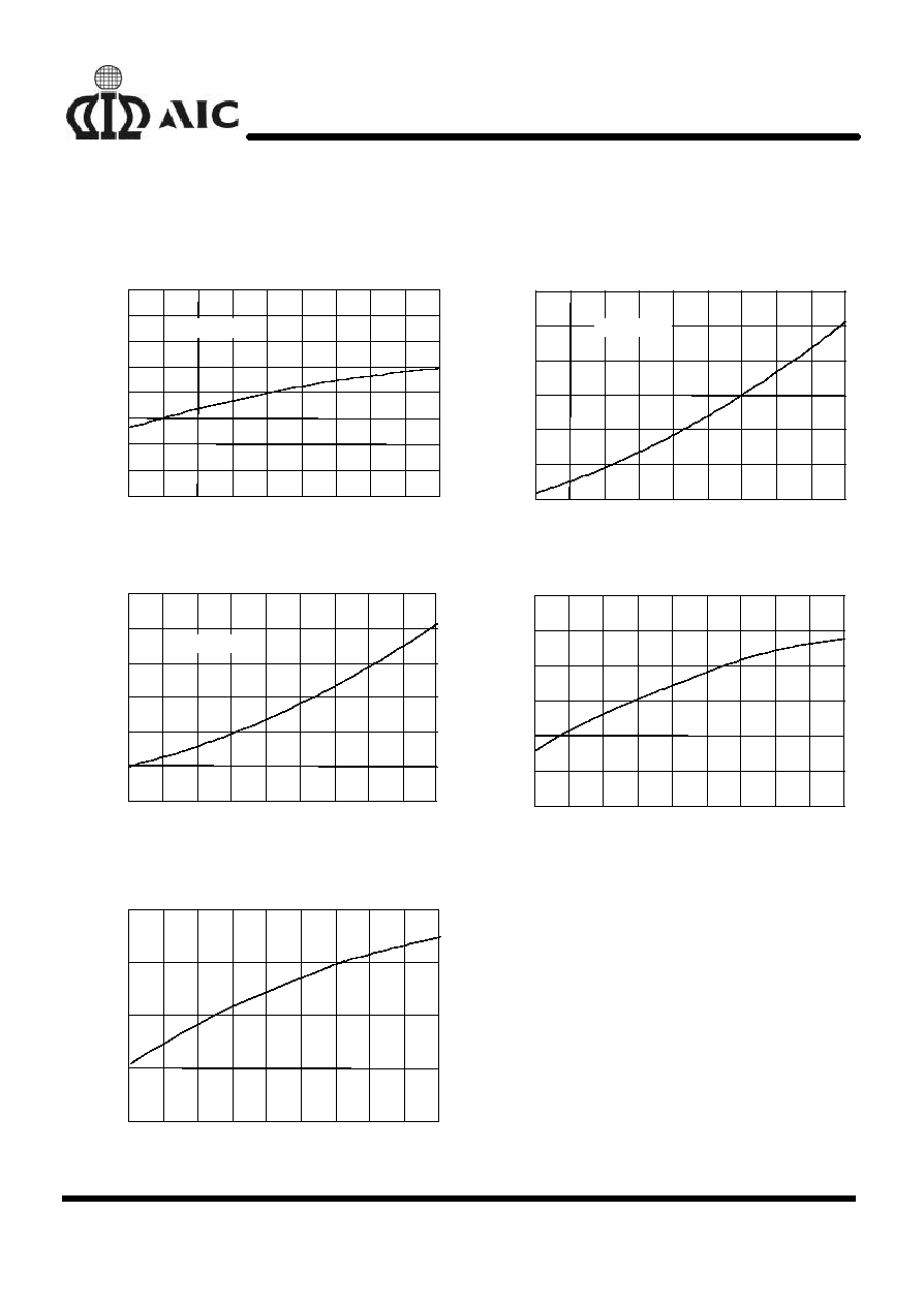
AIC1803
6
n
TYPICAL PERFORMANCE CHARACTERISTICS
(Continued)
148.0
148.5
149.0
149.5
150.0
150.5
151.0
151.5
152.0
Fig. 7 Overcurrent Protection Voltage vs. Temperature
Overcurrent Protection Voltage (V)
-20
-10
0
10
20
30
40
50
60
70
Temperature(
∞
C)
V
CELL
=3.5V
14
16
18
20
22
24
26
Fig. 8 Overcharge/Overdischarge Delay Time vs.
Temperature
-20
-10
0
10
20
30
40
50
60
70
C
TC
/C
TD
=1nF
Overcharge/Overdischarge Delay Time (
m
S)
Temperature(
∞
C)
-20
-10
0
10
20
30
40
50
60
70
10
12
14
16
18
20
22
V
CELL
=3.5V
Fig. 9 Overcurrent Delay Time 1 vs. Temperature
Overcurrent Delay Time 1 (
m
S)
Temperature (
∞
C)
Temperature (
∞
C)
-20
-10
0
10
20
30
40
50
60
70
4.02
4.03
4.04
4.05
4.06
4.07
4.08
Fig. 10 Overcharge Release Voltage vs. Temperature
Overcharge Release Voltage (V)
-20
-10
0
10
20
30
40
50
60
70
2.97
2.98
2.99
3.00
3.01
Fig. 11 Overdischarge Release Voltage vs. Temperature
Overdischarge Release Voltage (V)
Temperature (
∞
C)

AIC1803
7
n
BLOCK DIAGRAM
450
400
350
11
VC3
13
VC2
9
10
12
14
15
UD2
UD3
UD1
GND
VC1
Wake-up
Control
16
2
6
1
3
OC
OD
VCC
7
TC
TI
VCC-1V
VCC-0.3V
VCC-0.15V
VCC+0.4V
Power-Down
Control
1.2V
Overcharge
Delay Circuit
Overdischarge
Delay Circuit
Overcurrent
Delay Circuit
CS
5
TD
Battery
Voltage
Sense
Circuit

AIC1803
8
n
PIN DESCRIPTIONS
PIN 1: OC-
NMOS open drain output
for
control of the charge control
MOSFET M2. When overcharge
occurs, this pin sinks current to
switch the
external PNP Q1 on,
and charging is inhibited by
turning off the charge
control
MOSFET M2.
PIN 2: CS-
Input pin for current sensing.
Using the drain-source voltage of
the discharge control
MOSFET
M1 (voltage between
VCC and CS),
it senses
discharge current
during
normal mode and detects
whether charging current is
present
during power-down
mode.
PIN 3: OD -
Output pin for control of
discharge control MOSFET M1.
When overdischarge occurs, this
pin goes high to turn off the
discharge control MOSFET M1
and discharging is inhibited.
PIN 4: NC -
No connection
PIN 5: TD
-
Overdischarge delay time setting
pin.
PIN 6: TI
-
Overcurrent
delay
time setting
pin.
PIN 7: TC
-
Overcharge
delay time setting
pin.
PIN 8: NC
-
No connection.
PIN 9: GND
-
Ground pin. This pin is to be
connected to the negative
terminal of the battery cell BAT3.
PIN10: UD3 -
This pin is to be connected to the
positive terminal of the battery
cell BAT3 for cell-balancing
bleeding function under
overcharge condition.
PIN11: VC3-
Input pin for battery BAT3
voltage sensing. This pin is to be
connected to the positive
terminal of the battery cell BAT3.
PIN12: UD2 - This pin is to be connected to the
positive terminal of the battery
cell BAT2 for cell-balancing
bleeding function under
overcharge condition.
PIN13: VC2-
Input pin for battery BAT2
voltage sensing. This pin is to be
connected to the positive
terminal of the battery cell BAT2.
PIN14: UD1-
This pin is to be connected to the
positive terminal of the battery
BAT1 for cell-balancing
bleeding function under
overcharge condition.
PIN15: VC1-
Input pin for battery BAT1
voltage sensing. This pin is to be
connected to the positive
terminal of the battery cell BAT1.
PIN16: VCC -
Power supply pin. This pin is to
be connected to the positive
terminal of the battery cell BAT1.
n
APPLICATION INFORMATIONS
l
THE OPERATION
Initialization
On initial power-up, such as connecting the
battery pack for the first time to the AIC1803 , the
AIC1803 enters the power-down mode . A charger
must be applied to the AIC1803 circuit to enable
the pack.
Overcharge Protection
When the voltage of either of the battery cells
exceeds the overcharge protection voltage (V
OCP
)
beyond the overcharge delay time (T
OC
) period,
charging is inhibited by the turning-off of the
charge control MOSFET M2. The overcharge

AIC1803
9
delay time is set by the external capacitor C
TC
Inhibition of charging is immediately released
when the voltage of the overcharged cell becomes
lower than overcharge release voltage (V
OCR
or
V
OCP
-V
HYS
) through discharging.
Overdischarge Protection
When the voltage of either of the battery cells falls
below the overdischarge protection voltage (V
O D P
)
beyond the overdischarge delay time (T
OD
) period,
discharging is inhibited by the turning-off of the
discharge control MOSFET M1. The
overdischarge delay time is set by the external
capacitor C
T D
.
Inhibition of discharging is
immediately released when the voltage of the
overdischarge cell becomes higher than the
overdischarge release voltage (V
O D R
) through
charging.
Overcurrent Protection
In normal mode, the AIC1803 continuously
monitors the discharge current by sensing the
voltage of CS pin. If the voltage V
C C
-V
C S
exceeds
the overcurrent protection voltage (V
O I P
) beyond
the overcurrent delay time (T
O I
)
period, the
overcurrent protection circuit operates and
discharging is inhibited by the turning-off of the
discharge control MOSFET M1. Discharging must
be inhibited for at least 256mS after overcurrent
takes place to avoid damage to external control
MOSFETs due to rapidly switching transient
between BATT+ and BATT- terminals. The
overcurrent condition returns to normal mode
when the load is released and the impedance
between the BATT+ and BATT- terminals is
20M
or higher.
The AIC1803 is provided with the three
overcurrent detection levels (0.15V, 0.3V and
1.0V) and the three overcurrent delay time (T
O I 1
,
T
O I 2
and T
O I 3
) corresponding to each overcurrent
detection level. T
OI1
is set by the external capacitor
C
TI
. T
OI2
and T
OI3
default to 4mS and 300
µ
s
respectively, and can not be adjusted due to
protection of external MOSFETs
Cell-Balancing Bleeding after Overcharge
When either of the battery cells is overcharged,
the AIC1803 provides the cell-balancing bleeding
function to discharge the overcharged cell at
about 9mA until the voltage of the overcharged
cell decreases to overcharge release voltage
(V
OCR
or V
O C P
-V
H Y S
). This function is
accomplished by connecting UD1, UD2, UD3 pins
to the positive terminals of battery cells BAT1,
BAT2, BAT3 respectively. The bleeding current
can be decreased by inserting resistors along
UD1 pin to BAT1 positive terminal path and UD3
pin to BAT3 positive terminal path.
Power-Down after Overdischarge
When overdischarge occurs, the AIC1803 will go
into power-down mode, turning off all the timing
generation and detection circuitry to reduce the
quiescent current to about 1.3
µ
A (V
CC
=6.9V). In
the unusual case where one battery cell is
overdischarged while another one under
overcharge condition, the AIC1803 will turn off all
the detection circuitry except the overcharge
detection circuit for the cell under overcharge
condition.
Charge Detection after Overdischarge
When overdischarge occurs, the discharge control
MOSFET M1 turns off and discharging is inhibited.
However, charging is still permitted through the
parasitic diode of M1. Once the charger is
connected to the battery pack, the AIC1803
immediately turns on all the timing generation and
detection circuitry and goes into normal mode.
Charging is determined to be in progress if the CS

AIC1803
10
pin voltage is higher than VCC + 0.4V (charge
detection threshold voltage V
C H
).
∑
DESIGN GUIDE
Setting the Overcharge and Over-
discharge Delay Time
The overcharge delay time is set by the external
capacitor C
T C
and the overdischarge delay time is
set by the external capacitor C
TD
.
The relationship
between capacitance of the external capacitors
and delay time is tabulated as below.
C
TC
,C
T D
(F)
1n
5n
10n
22n
33n
T
OC
,T
OD
(S)
21m
52m
132m
253m
347m
C
TC
,C
T D
(F)
47n
68n
82n
100n
T
OC
,T
OD
(S)
617m
748m
1004m
1630m
The delay time can also be approximately
calculated by the following equations (if C
T C
, C
TD
82nF) :
T
OC
(mS)
=
11.8 x C
TC
(nF)
T
OD
(mS)
=
11.8 x C
TD
(nF)
Setting the Overcurrent Delay Time 1
The overcurrent delay time 1 (T
O I 1
) at 0.15V
<
V
C C
-
V
C S
< 0.3V is set by the external capacitor
C
TI
, while the overcurrent delay time 2 and 3 (T
O I 2
and T
O I 3
) is fixed by IC internal circuit.The
relationship between capacitance of the external
capacitor and delay time is tabulated as below.
C
TI
(F)
1n
2.2n
3.3n
5n
6.8n
10n
T
OI
(mS)
4.8
15.0
18.8
23.6
31.0
61.8
Selection of External Control MOSFETs
Because the overcurrent protection voltage is
preset, the threshold current for overcurrent
detection is determined by the turn-on resistance
of the discharge control MOSFET M1. The turn-on
resistance of the external control MOSFETs can
be determined by the equation: R
ON
= V
O I P
/ I
T
(I
T
is the overcurrent threshold current). For example,
if the overcurrent threshold current I
T
is designed
to be 5A, the turn-on resistance of the external
control MOSFETs must be 30m
. Users should
be aware that turn-on resistance of the MOSFET
changes with temperature variation due to heat
dissipation. It changes with the voltage between
gate and source as well. (Turn-on resistance of a
MOSFET increases as the voltage between gate
and source decreases). Once the turn-on
resistance of the external MOSFET changes, the
overcurrent threshold current will change
accordingly.
Suppressing the Ripple and Disturbance
from Charger
To suppress the ripple and disturbance from
charger, connecting R1 to R4 and C1 to C4 is
recommended.
Controlling the Charge Control MOSFET
R5, R6, R7 and NPN transistor Q1 are used to
switch the charge control MOSFET M2. If
overcharge does not occur, no current flows into
OC pin and Q1 is turned off, then M2 is turned on.
When overcharge occurs, current flows into OC
pin and Q1 is turned on, which turns off M2 in turn.
Protection at CS Pin
R8 is used for protection of IC when charger is
connected in reverse. The charge detection
function after overdischarge is possibly disabled
by larger value of R8. Resistance of 1K
is
recommended.

AIC1803
11
n
TIMING DIAGRAM
l
Overcharge and Overdischarge Protection (V
CS
=V
CC
)
OD
T
0V
0V
BAT3
BAT2
BAT1
V
V
V
CELL
OD
<T
OC
<T
T
OC
Hi-Z
Hi-Z
V
V
OC
V
OD
CC
V
OCP
V
ODP
V
ODR
V
HYS
V
OCP
V
-
l
Overcurrent Protection (V
CELL
=3.5V)
V
CC
0V
CC
V
0V
- 1V
- 0.3V
- 0.15V
OI1
T
V
CC
CC
V
CC
V
OC
V
OD
V
CS
V
<256ms
<256ms
256ms
Hi-Z
<T
OI1
OI3
<T
OI2
>256ms
T

AIC1803
12
n
PHYSICAL DIMENSIONS
l
16 LEAD PLASTIC SO (150 mil) (unit: mm)
SYMBOL
MIN
MAX
A
1.35
1.75
A1
0.10
0.25
B
0.33
0.51
C
0.19
0.25
D
9.80
10.00
E
3.80
4.00
e
1.27 (TYP)
H
5.80
6.20
L
0.40
1.27
E
e
D
B
C
A
A1
L
H