MC34063A
Industrial Standard, Universal DC/DC Converter
Analog Integrations Corporation
4F, 9 Industry E. 9th Rd, Science-Based Industrial Park, Hsinchu, Taiwan
DS-34063A-01 012102
TEL: 886-3-5772500
FAX: 886-3-5772510
www.analog.com.tw
1
n
FEATURES
l
3V to 30V Input Voltage Operation.
l
Internal 1.6A Peak Current Switch.
l
Internal
�
1.8% Reference.
l
Low Quiescent Current at 1.6mA.
l
Frequency Operation from 100Hz to 100KHz.
l
Current Limiting.
n
APPLICATIONS
l
Saver for Cellular phones
l
DC-DC Converter Module
n
DESCRIPTION
The MC34063A by Analog Integrations
Corporation, an improved second source over the
industrial standard MC34063A, is a monolithic
control circuit containing the primary functions
required for DC/DC converters. The device
consists of an internal temperature compensated
reference, comparator, controlled duty cycle
oscillator with an active current limit circuit, driver
and high current output switch. This device is
specifically designed to be incorporated in step-
down, step-up and voltage-inverting applications
with a minimum number of external components.
The
�
1.8% internal reference and low quiescent
current of 1.6mA are among the improvements of
the device over the competition.
n
TYPICAL APPLICATION CIRCUIT
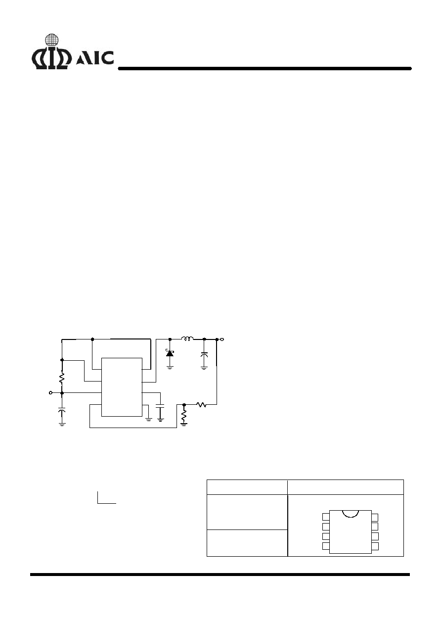
MC34063A
IPK
8
7
6
5
4
3
2
1
FB
VCC
DRI
SC
SE
TC
GND
V
IN
L
200
�
H
RB
33K
C1
D1
1N5819
CT
470pF
RA
5.6K
*RS
V
OUT
8.6V SAVER
*:Io=0.3/RS
+
100
�
F
220
�
F
C
O
+
Saver Circuit for Cellular Phone
n
ORDERING INFORMATION
MC34063A CX
ORDER NUMBER
MC34063ACN
(PLASTIC DIP)
PIN CONFIGURATION
MC34063ACS
(PLASTIC SO)
TOP VIEW
VCC
DRI
SE
TC
GND
IPK
FB
SC
1
3
4
2
8
6
5
7
PACKAGE TYPE
N: PLASTIC DIP
S: SMALL OUTLINE

MC34063A
2
n
ABSOLUTE MAXIMUM RATINGS
Supply Voltage
......................................................... ... ... ... .....................................
30V
Comparator Input Voltage Range
..................................... ... ... ... .................... -0.3V~30V
Switch Collector Voltage
.......................................... ... ... ... ... ......................................30V
Switch Emitter Voltage
..................................... ... ... ... ... .............................................30V
Switch Collector to Emitter Voltage
........................ ... ... ... ..........................................30V
Driver Collector Voltage
.................................... ... ... ... ... ............................................30V
Switch Current
............................................... ... ... ... ... ..............................................1.6A
Power Dissipation and Thermal Characteristics
DIP Package
T
A
= 25
�
C
.................................. ... ... ... .............................1.0W
Thermal Resistance .................... ... ... .......................100
�
C /W
SO Package
T
A
= 25
�
C
.................................... ... ... ... ... .......................625mW
Thermal Resistance .................... ... ... .......................160
�
C /W
Operating Junction Temperature ................................... ... ... ... ..... .............................125
�
C
Operating Ambient Temperature Range .................... ... ...... ...............................0
�
C~70
�
C
Storage Temperature Range ........................ ... ... ... ... ....... ........................... - 65
�
C~150
�
C

MC34063A
3
n
ELECTRICAL CHARACTERISTICS
(VCC= 5V, T
A
=25
�
C, unless otherwise
specified.)
PARAMETER
TEST CONDITIONS
SYMBOL MIN. TYP. MAX. UNIT
Oscillator
Charging Current
5.0V
VCC
30V
I
CHG
10
25
40
�
A
Discharge Current
5.0V
VCC
30V
I
DISCHG
100
150
200
�
A
Voltage Swing
PIN 3
V
OSC
0.6
V
Discharge to Charge Current
Ratio
V
IPK(SENSE)
=VCC
I
DISCHG/
I
CHG
6.0
Current Limit Sense Voltage
I
CHG
=I
DISCHG
V
IPK(SENSE)
250
300
350
mV
Output Switch
Saturation Voltage,
Darlington Connection
I
SW
=1.0A;
V
C(DRIVER)
=V
C(SWITCH)
V
CE(SAT)
1.0
1.3
V
Saturation Voltage
I
SW
=1.0A; I
C(DRIVER)
=50mA
(Forced
20)
V
CE (SAT)
0.4
0.7
V
DC Current Gain
I
SW
=1.0A; V
CE
=5.0V
h
FE
35
120
Collector Off-State Current
V
CE
=30V
I
C(OFF)
10
nA
Comparator
Threshold Voltage
Threshold Voltage
T
A
=25
�
C
0
�
C
T
A
70
�
C
V
FB
1.227
1.21
1.25
1.273
1.29
V
Threshold Voltage Line
Regulation
3.0V
VCC
30V
REG
LINE
0.1
0.3
mV/V
Input Bias Current
V
IN
=0V
I
IB
0.4
1
�
A
Supply current
V
IPK(SENSE)
=VCC
V
PIN 5
>V
FB
5.0V
VCC
30V
C
T
=0.001
�
F, PIN 2=GND
Remaining pins open
I
CC
1.6
3
mA
MC34063A
4
n
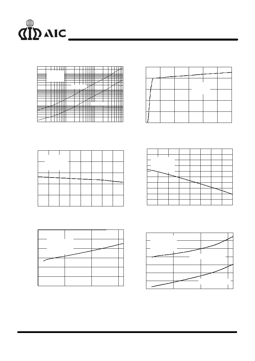
TYPICAL PERFORMANCE CHARACTERISTICS
C
T
, Oscillator Timing Capacitor (nF)
t
ON
-OFF
Output Switch ON-OFF Time
Fig. 1 Output Switch ON-OFF Time vs. Oscillator
Timing Capacitor
0.1
1
10
100
1
10
OFF TIME
VCC=5V
V
IPK
=VCC
PIN
5=GND
100
1000
ON TIME
0
5
10
15
20
25
30
0
0.4
0.8
1.2
1.6
2
C
T
=1nF
V
IPK
= VCC
PIN 2=GND
VCC, Supply Voltage (V)
I
CC
, Suppl
y C
u
rrent (
mA)
Fig. 2 Standby Supply Current vs. Supply Voltage
Fig. 3 V
FB
, Threshold Voltage vs. Temperature
0
10
20
30
40
50
60
70
80
1.2
1.
22
1.24
1.26
1.28
1.3
VCC = 5V
C
T
=1nF
Pin 2= GND
Temperature (
�
C)
V
FB
, Threshold Voltage (V)
250
260
270
280
290
300
310
320
330
340
350
Fig. 4 IPK Threshold Voltage vs. Temperature
Temperature (
�
C)
V
IPK
, Threshold
Voltage (mV)
0
10
20
30
40
50
60
70
80
VCC = 5V
C
T
=1nF
Pin 5= GND
Fig. 5 Emmiter-Follower Configuration Output
Switch Saturation Voltage vs. Emmiter Current
I
E
, Emitter Current (A)
1.2
1.3
1.4
1.5
1.6
1.7
1.8
V
CE(
SAT)
Saturation
Voltage (V)
0
0.5
1
1.5
VCC = 5V
Pin 1, 7, 8=VCC
Pin 3, 5= GND
I
C
, Collector Current (A)
1.5
Fig. 6 Common-Emitter Configuration Output
Switch Saturation Voltage vs. Collector Current
0
0.2
0.4
0.6
0.8
1.0
1.2
1.4
0
0.5
1
Forced Beta = 20
V
CE(
SAT)
Saturation Voltage (V)
Darlington Connection
VCC = 5V
Pin 1, 7, 8=VCC
Pin 3, 5= GND
MC34063A
5
n
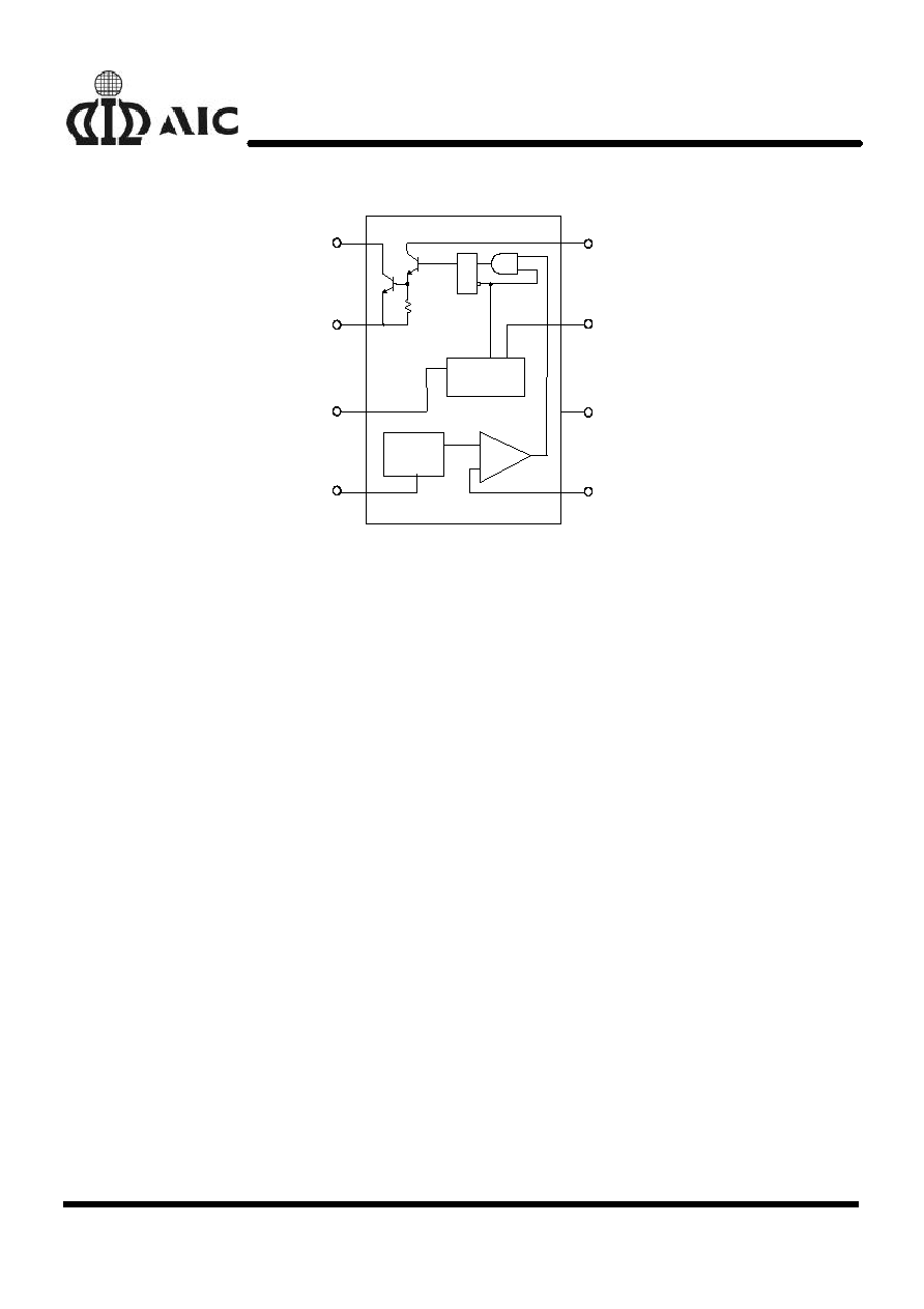
BLOCK DIAGRAM
Q
R
S
8
7
6
5
4
3
2
1
Q1
IS
CT
-
+
Q2
80
DRI
IPK
VCC
FB
GND
TC
SC
SE
Oscillator
Comparator
1.25V
Reference
Voltage
n
PIN DESCRIPTIONS
PIN 1: SC
- The switch collector is 1.6A.
PIN 2: SE
- Darlington switch emitter
PIN 3: TC
- Oscillator timing capacitor
PIN 4: GND - Power GND
PIN 5: FB
- Feedback comparator inverting input
PIN 6: VCC - Power supply input
PIN 7: IPK - Highside current sense input,
VCC - V
IPK
=300mV
PIN 8: DRI - Drive collector

MC34063A
6
n
APPLICATION INFORMATION
�
DESIGN FORMULA TABLE
CALCULATION
STEP-DOWN
STEP-UP
VOLTAGE-INVERTING
OFF
ON
t
t
V + V
V
- V - V
OUT
F
IN(MIN)
SAT
OUT
V + V
V
V
- V
OUT
F
IN(MIN)
IN(MIN)
SAT
-
V
+ V
V - V
OUT
F
IN
SAT
(t
ON
+ t
OFF
)
MAX
1
F
MIN
1
F
MIN
1
F
MIN
C
T
4x10
-5
t
ON
4 x 10
-5
t
ON
4 x 10
-5
t
ON
I
C (SWITCH)
2I
OUT(MAX)
2I
OUT(MAX)
(
)
t + t
t
ON
OFF
OFF
2I
OUT(MAX)
(
)
t + t
t
ON
OFF
OFF
RS
0.33/I
C(SWITCH)
0.33/ I
C (SWITCH)
0.33/ I
C (SWITCH)
L(MIN)
(
)
V
- V - V
I
t
IN(MIN)
SAT
OUT
C(SWITCH)
ON(MAX)
(
)
V
- V
I
t
IN(MIN)
SAT
C(SWITCH)
ON(MAX)
(
)
V
- V
I
t
IN(MIN)
SAT
C(SWITCH)
ON(MAX)
Co
I
(t + t
8V
C ( SWITCH)
ON
OFF
RIPPLE (P - P )
)
I t
V
OUT
ON
RIPPLE(P - P)
I t
V
OUT
ON
RIPPLE(P - P)
V
SAT
- Saturation voltage of the output switch.
V
F
- Forward voltage drop of the ringback
rectifier
The following power supply characteristics must
be chosen:
V
IN
-
Nominal input voltage.
V
OUT
-
Desired output voltage,
V
OUT
=1.25 (1 + RB/RA)
I
OUT
-
Desired output current.
F
MIN
-
Minimum desired output switching
frequency at the selected values for V
IN
and I
OUT
.
V
RIPPLE (P-P)
-
Desired peak-to-peak output ripple
voltage. In practice, the calculated value
will need to be increased due to the
capacitor equivalent series resistance and
board layout. The ripple voltage should be
kept to a low value since it will directly
effect the line and load regulation.
MC34063A
7
n
APPLICATION EXAMPLES
MC34063A
8
7
6
5
4
3
2
1
DRI
IPK
FB
VCC
SC
SE
TC
GND
L
200
�
H
RB
3K6
C1
C
O
470
�
F
D1
1N5821
CT
470pF
RA
1K2
RS
0.25
V
OUT
V
IN
5V/500mA
+
100
�
F
+
10~20V
Line Regulation
V
IN
= 10V ~20V @ I
O
=500mA
40mV
Load Regulation
V
IN
= 15V, @ I
O
=10mA ~ 500mA
5mV
Short Circuit Current
V
IN
=15V, @ R
L
= 0.1
1.3A
Fig. 1 Step-Down Converter
7
6
5
4
3
2
1
8
RS
0.22
C1
100
�
F
+
RA
RB
CT
470pF
R2
R1
1K
Q1
L
Co
+
D1
MC34063A
DRI
IPK
FB
VCC
SC
SE
TC
GND
V
OUT
5V/500mA
V
IN
470
10~22V
1K2
3K6
1N5821
470
�
F
200
�
H
Fig. 2 Step-Down Converter with External PNP Saturation Switch

MC34063A
8
n
APPLICATION EXAMPLES
(Continued)
D1
8
7
6
5
4
3
2
1
L
200
�
H
RB
47K
RA
2.2K
C1
C
O
220
�
F
CT
100pF
RS
0.22
28V/200mA
GS SS14
100
�
F
+
+
R1
100
MC34063A
DRI
IPK
FB
VCC
SC
SE
TC
GND
V
OUT
V
IN
8~16V
Line Regulation
V
IN
= 8V ~16V @ I
O
=200mA
100mV
Load Regulation
V
IN
= 12V, @ I
O
=80mA ~ 200mA
5mV
Fig. 3 Step-Up Converter
8
7
6
5
4
3
2
1
+
RS
C1
+
R2
RA
CT
RB
R1
Q1
L
C
O
D1
MC34063A
DRI
IPK
FB
VCC
SC
SE
TC
GND
V
OUT
V
IN
Fig. 4 Step-Up Converter with External NPN Switch

MC34063A
9
n
APPLICATION EXAMPLES
(Continued)
D1
1N5819
RB
8.2K
RA
953
C1
100
�
F
C
O
470
�
F
CT
680pF
S
RS
0.25
8
7
6
5
4
3
2
1
-12V/100mA
4.5V~6V
+
+
L
100
�
H
MC34063A
SC
SE
GND
TC
DRI
IPK
VCC
FB
V
OUT
V
IN
Line Regulation
V
IN
= 4.5V ~6V @ I
O
=100mA
20mV
Load Regulation
V
IN
= 5V, @ I
O
=10mA ~ 100mA
100mV
Fig.5 Inverting Converter
8
7
6
5
4
3
2
1
+
+
RS
C1
R2
RB
CT
RA
R1
Q1
L
CO
D1
MC34063A
DRI
IPK
FB
VCC
SC
SE
TC
GND
V
OUT
V
IN
Fig 6. Voltage Inverting Converter with PNP Saturated Switch

MC34063A
10
n
PHYSICAL DIMENSIONS
l
8 LEAD PLASTIC SO (unit: mm)
SYMBOL
MIN
MAX
A
1.35
1.75
A1
0.10
0.25
B
0.33
0.51
C
0.19
0.25
D
4.80
5.00
E
3.80
4.00
e
1.27(TYP)
H
5.80
6.20
L
0.40
1.27
D
H
e
A
B
A1
C
E
L
l
8 LEAD PLASTIC DIP (unit: mm)
SYMBOL
MIN
MAX
A1
0.381
--
A2
2.92
4.96
b
0.35
0.56
C
0.20
0.36
D
9.01
10.16
E
7.62
8.26
E1
6.09
7.12
e
2.54 (TYP)
eB
--
10.92
b
e
L
A2
A1
eB
E
C
E1
D
L
2.92
3.81