 | –≠–ª–µ–∫—Ç—Ä–æ–Ω–Ω—ã–π –∫–æ–º–ø–æ–Ω–µ–Ω—Ç: TL431ACS | –°–∫–∞—á–∞—Ç—å:  PDF PDF  ZIP ZIP |

AIC431/TL431A/TL431
Adjustable Precision Shunt Regulators
Analog Integrations Corporation 4F, 9, Industry E. 9th Rd, Science Based Industrial Park, Hsinchu Taiwan, ROC
www.analog.com.tw
DS-431-06 May 31, 01
TEL: 886-3-5772500 FAX: 886-3-5772510
1
n
FEATURES
l
Unconditionally Stable.
l
Precision Reference Voltage.
AIC431
:2.495V
±
0.5%
TL431A :2.495V
±
1.0%
TL431
:2.495V
±
1.6%
l
Sink Current Capability: 200mA.
l
Minimum Cathode Current for Regulation: 250
µ
A.
l
Equivalent Full-Range Temperature Coefficient:
50 ppm/
∞
C.
l
Fast Turn-On Response.
l
Low Dynamic Output Impedance: 0.08
.
l
Adjustable Output Voltage.
l
Low Output Noise.
l
Space Saving SOT-89, SOT-23, TO-92 and SO8
packages.
n
TYPICAL APPLICATION CIRCUIT
V
IN
AIC431
+
V
OUT
R1
R2
+
V
OUT
=(1+R1/R2)V
REF
Precision Regulator
n
DESCRIPTION
The AIC431/TL431A/TL431 are 3-terminal ad-
justable precision shunt regulators with guar-
anteed temperature stability over the applica-
ble extended commercial temperature range.
The output voltage may be set at any level
greater than 2.495V (V
REF
) up to 30V merely
by selecting two external resistors that act as
a voltage divider network. These devices have
a typical output impedance of 0.08
. Active
output circuitry provides a very sharp turn-on
characteristics, making these devices excel-
lent improved replacements for zener diodes
in many applications.
The precise
±
0.5% reference voltage toler-
ance of the AIC431 makes it possible in
many applications to avoid the use of a vari-
able resistor, consequently saving cost and
eliminating drift and reliability problems asso-
ciated with it.

AIC431/TL431A/TL431
2
n
ORDERING INFORMATION
ORDER NUMBER
PIN CONFIGURATION
AIC431 CX
TL431A CX
TL431
CX
PACKAGING TYPE
S: SMALL OUTLINE
U: SOT-23
X: SOT-89
Z: TO-92
AIC431CX
TL431ACX
TL431CX
(SOT-89)
FRONT VIEW
1: VREF
2: ANODE
3: CATHODE
1
2
3
1
2
3
AIC431CZ
TL431ACZ
TL431CZ
(TO-92)
FRONT VIEW
1: VREF
2: ANODE
3: CATHODE
ANODE
REF
ANODE
NC
ANODE
ANODE
NC
CATHOD
1
3
4
2
8
6
5
7
AIC431CS
TL431ACS
TL431CS
(SO-8)
TOP VIEW
AIC431CUN
TL431ACUN
TL431CUN
(SOT-23)
FRONT VIEW
1: CATHODE
2: VREF
3: ANODE
1
3
2
AIC431CUS
TL431ACUS
TL431CUS
(SOT-23)
FRONT VIEW
1: VREF
2: CATHODE
3: ANODE
3
1
2
n
ABSOLUTE MAXIMUM RATINGS
Cathode Voltage ........... ... ... ... ... .................. ... ... ... ... ..... ... ... ...............................30V
Continuous Cathode Current ...................... ... ... ... .... ... ...................... -10mA ~ 250mA
Reference Input Current Range
.......... ... ... ... ........... ... ............. ... ... ... ... ... ... ... 10mA
Operating Temperature Range .......... ... ... ... ............ ... ... ............ ... ... ... ... . -40
∞
C ~ 85
∞
C
Lead Temperature .......... ... ... ... ..................... ... ... ... ... ... ..... ... ... ... ... ... ... ... ... . 260
∞
C
Storage Temperature .......... ... ... ... ..................... ... ... ... ... ..... ... ... ... ... .. -65
∞
C ~ 150
∞
C
Power Dissipation (Notes 1, 2)
SOT-89 Package ............ ... ... ... ...... 0.80W
TO-92 Package ... .......... ... ... ... ....... 0.78W
Note 1: TJ, max = 150
∞
C.
Note 2: Ratings apply to ambient temperature at 25
∞
C.
AIC431/TL431A/TL431
3
n
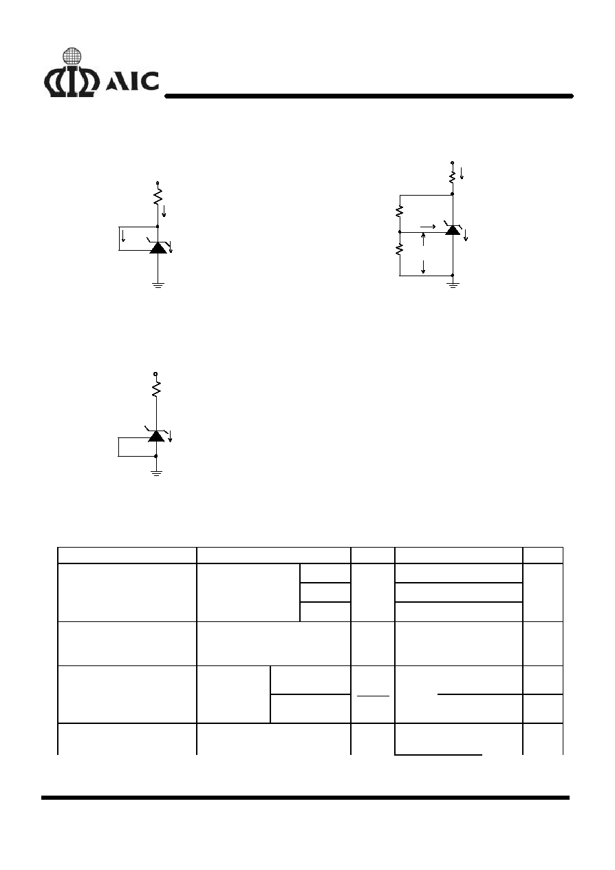
TEST CIRCUITS
V
REF
I
REF
I
Z
V
Z
I
L
IN
AIC431
R2
R1
V
REF
I
REF
I
Z
V
Z
IN
I
L
AIC431
Note: V
Z
=V
REF
(1+R1/R2)+I
REF
xR1
Fig. 1 Test Circuit for V
Z
=V
REF
Fig. 2 Test circuit for V
Z
>V
REF
IN
V
Z
I
Z(OFF)
AIC431
Fig. 3 Test circuit for off-state Current
n
ELECTRICAL CHARACTERISTICS
(Ta=25
∞
C, unless otherwise specified.)
PARAMETER
TEST CONDITIONS
SYMBOL
MIN.
TYP.
MAX.
UNIT
V
Z
=V
REF
,
AIC431
2.482
2.495
2.508
IL =10mA (Fig. 1)
TL431A
2.470
2.495
2.520
Reference Voltage
TL431
V
REF
2.455
2.495
2.535
V
Deviation of Reference
Input Voltage Over
Temperature (Note 3)
V
Z
= V
REF
, I
L
=10mA,
Ta
= 0
∞
C~ +85
∞
C (Fig. 1)
V
DEV
9.0
20
mV
Ratio of the Change in Refer-
ence Voltage to
I
Z
=10mA
V
Z
=10V-V
REF
-0.5
-2.0
mV/V
the Change in Cathode volt-
age
(Fig. 2)
V
Z
=30V-10V
V
REF
V
Z
-0.35
-1.5
mV/V
Reference Input Current
R1
=10K
, R2=
,
I
L
=10mA (Fig. 2)
I
REF
0.8
3.5
µ
A
AIC431/TL431A/TL431
4
Deviation of Reference Input
Current over Temperature
R1
=10K
, R2=
,
I
L
=10mA
Ta
=-20
∞
C ~ +85
∞
C (Fig. 2)
I
REF
0.3
1.2
µ
A

AIC431/TL431A/TL431
5
n
ELECTRICAL CHARACTERISTICS
(Continued)
PARAMETER
TEST CONDITIONS
SYMBOL
MIN.
TYP.
MAX.
UNIT
Minimum Cathode current for
Regulation
V
Z
=V
REF
(Fig. 1)
I
Z(MIN)
0.25
0.5
mA
Off-State Current
V
Z
=20V, V
REF
=0V (Fig. 3)
I
Z(OFF)
0.1
1.0
µ
A
Dynamic Output Impedance
(Note 4)
V
Z
=V
REF
Frequency= 0Hz (Fig. 1)
R
Z
0.08
0.3
T
2
T
1
V
MAX
V
DEV
= V
MAX
-V
MIN
V
MIN
TEMPERATURE
Note 3. Deviation of reference input voltage, V
DEV
, is de-
fined as the maximum variation of the reference input
voltage over the full temperature range.
The average temperature coefficient of the reference in-
put voltage,
V
REF
is defined as:
T1
T2
10
C)
25
(at
V
V
T1
T2
6
10
C)
25
(at
V
V
-
V
C
ppm
V
6
REF
DEV
REF
MIN
MAX
REF
-
∞
±
=
-
∞
±
=
∞
Where:
T
2
-
T
1
=full temperature change.
V
REF
can be positive or negative depending on
whether the slope is positive or negative.
Example: V
DEV
= 9.0mV, V
REF
= 2495mV,
T
2
-
T
1
= 70
∞
C, slope is negative.
C
50ppm/
V
C
70
6
10
2495mV
9.0mV
REF
∞
-
=
=
∞
Note 4. The dynamic output impedance, Rz, is de-
fined as:
R
Z
=
Z
Z
V
I
When the device is programmed with two external re-
sistors, R1 and R2, (see Fig. 2), the dynamic output
impedance of the overall circuit, is defined as:
[ ]
R2
R1
1
Rz
Iz
Vz
z
r
+
=
n
TYPICAL PERFORMANCE CHARACTERISTICS
-1.0
-0.5
0.0
0.5
1.0
1.5
2.0
2.5
3.0
-600
-400
-200
0
200
400
600
800
1000
I
Z(MIN)
V
Z
=V
REF
T
A
=25
∞
C
Cathode Current vs Cathode Voltage
Cathode Current (
µ
A)
Cathode Voltage (V)
-40
-20
0
20
40
60
8 0
100
120
2.40
2.42
2.44
2.46
2.48
2.50
2.52
2.54
2.56
2.58
Reference Voltage vs Temperature
V
Z
=V
REF
I
Z
=10mA
Reference
Voltage (V)
Temperature (
∞
C)
V
REF
=2.535V
V
REF
=2.495V
V
REF
=2.455V