
ASAHI KASEI
[AK4101A]
MS0250-E-00
2003/07
- 1 -
GENERAL DESCRIPTION
The AK4101A is a four outputs digital audio transmitter (DIT) which supports data rate up to 192kHz
sample rate operation. The AK4101A supports AES3, IEC60958, S/PDIF & EIAJ CP1201 interface
standards. The AK4101A accepts audio data and auxiliary information data and etc, which is then
biphase-encoded and driven on to a cable. The audio serial port supports eight formats.
FEATURES
o
Sampling Rate up to 192kHz
o
Support AES3, IEC60958, S/PDIF & EIAJ CP1201 professional and consumer formats
o
Generates CRCC codes and parity bits
o
Four on-chip RS422 line drivers
o
64-byte on-chip buffer memory for Channel Status and User bits
o
Supports synchronous/asynchronous access to Channel Status and User bits
o
Supports multiple clock frequencies: 128fs, 256fs, 384fs and 512fs
o
Supports Left/Right justified and I
2
S audio formats
o
Easy to use 4 wire, Serial Host Interface
o
Audio Routing Mode (Transparent Mode)
o
Power supply: 4.75 to 5.25V
o
TTL level I/F
o
Small Package: 44pin LQFP
o
Temperature range of - 40 to 85
�
C
Quad Outputs 192kHz 24-Bit DIT
AK4101A

ASAHI KASEI
[AK4101A]
MS0250-E-00
2003/07
- 2 -
n
Block Diagram
Host Serial
Interface
Audio Serial
Interface
BICK
LRCK
SDTI1
TXP1
MUX
CRCC Generator
Prescaler
RS422 Line Drivers
Biphase
Encoder
SDTI2
SDTI3
SDTI4
DIF2
Drivers
DIF1
Drivers
DIF0
Drivers
CKS1
Drivers
CKS0
MCLK
BLS
TRANS
VSS
Drivers
VDD
Drivers
TXN1
TXP2
TXN2
TXP3
TXN3
TXP4
TXN4
C1
C2
C3
C4
U1
U2
U3
U4
V12
V34
FS0
FS1
FS2
FS3
Register
CSN
CCLK
CDTI
CDTO
ANS
PDN
ASAHI KASEI
[AK4101A]
MS0250-E-00
2003/07
- 3 -
n
Ordering Guide
AK4101AVQ -40
+85
�
C 44pin LQFP (0.8mm pitch)
n
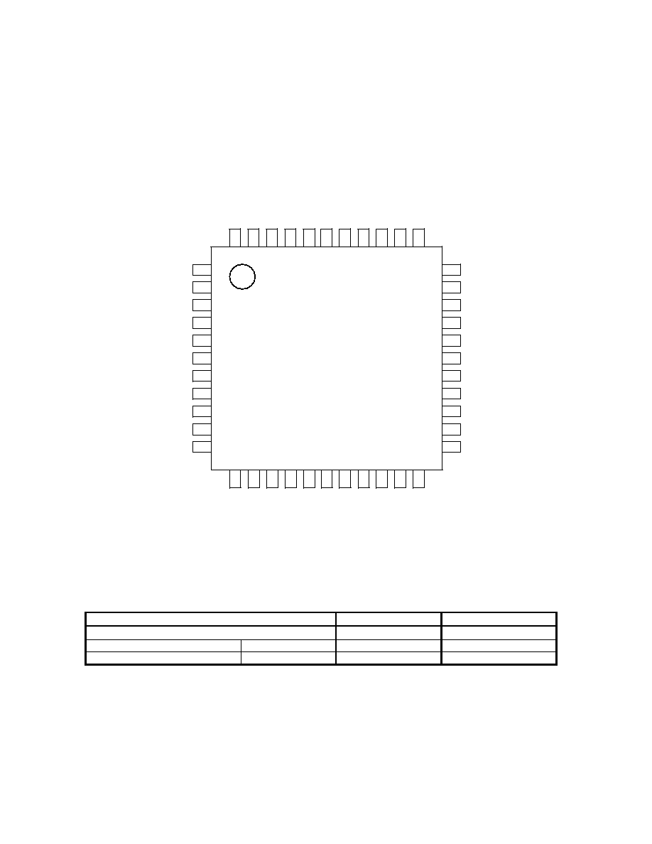
Pin Layout
PDN
TRANS
1
MCLK
2
SDTI1
3
SDTI2
4
SDTI3
5
SDTI4
6
VDD
7
VSS
8
BICK
9
LRCK
10
FS0/CSN
11
V34
V12
U2
U1
DIF2
DIF1
VDD
DIF0
FS1/CDTI
FS2/CCLK
FS3/CDTO
C1
C2
C4
ANS
BLS
CKS0
VSS
33
32
31
30
29
28
27
26
25
24
23
TXP1
TXN1
TXP2
TXN2
VSS
VDD
TXP3
TXN3
TXP4
TXN4
CKS1
AK4101AVQ
Top View
C3
U4
U3
44
43
42
41
40
39
38
37
36
35
34
12
13
14
15
16
17
18
19
20
21
22
n
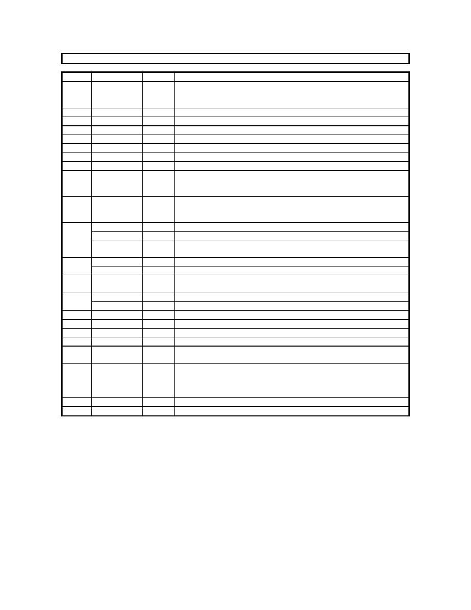
Comparison AK4101 with AK4101A
Function
AK4101
AK4101A
Ambient Temperature
-10 ~ 70
�
C
-40 ~ 85
�
C
CRCC generation by FS3-0 pins
Synchronous mode
X
O
CRCC generation by FS3-0 bits
Asynchronous mode
X
O
O: Input data is reflected to CRCC.
X: Input data is ignored for CRCC.
ASAHI KASEI
[AK4101A]
MS0250-E-00
2003/07
- 4 -
PIN/FUNCTION
No.
Pin Name
I/O
Function
1
PDN
I
Power Down & Reset Pin (Pull-up Pin)
When "L", the AK4101A is powered-down, TXP/N pins are "L" and the
control registers are reset to default values.
2
MCLK
I
Master Clock Input Pin
3
SDTI1
I
Audio Serial Data Input 1 Pin
4
SDTI2
I
Audio Serial Data Input 2 Pin (Pull-down Pin)
5
SDTI3
I
Audio Serial Data Input 3 Pin (Pull-down Pin)
6
SDTI4
I
Audio Serial Data Input 4 Pin (Pull-down Pin)
7
VDD
-
Power Supply Pin, 4.75V
5.25V
8
VSS
-
Ground Pin, 0V
9
BICK
I/O
Audio Serial Data Clock Input/Output Pin
Serial Clock for SDTI pins which can be configured as an output based on
the DIF2-0 inputs.
10
LRCK
I/O
Input/Output Channel Clock Pin
Indicates left or right channel, and can be configured as an output based on
the DIF2-0 inputs.
FS0
I
Sampling Frequency Select 0 Pin at Synchronous mode (Pull-down Pin)
CSN
I
Host Interface Chip Select Pin at Asynchronous mode (Pull-down Pin)
11
AKMODE
I
AK4112B Mode Pin at Audio routing mode (Pull-down Pin)
0: Non-AKM receivers mode, 1: AK4112B mode
FS1
I
Sampling Frequency Select 1 Pin at Synchronous mode (Pull-down Pin)
12
CDTI
I
Host Interface Data Input Pin at Asynchronous mode (Pull-down Pin)
FS2
I
Sampling Frequency Select 2 Pin at Synchronous mode (Pull-down Pin)
13
CCLK
I
Host Interface Bit Clock Input Pin at Asynchronous mode (Pull-down Pin)
FS3
I
Sampling Frequency Select 3 Pin at Synchronous mode (Pull-down Pin)
14
CDTO
O
Host Interface Data Output Pin at Asynchronous mode (Pull-down Pin)
15
C1
I
Channel Status Bit Input Pin for Channel 1
16
C2
I
Channel Status Bit Input Pin for Channel 2 (Pull-down Pin)
17
C3
I
Channel Status Bit Input Pin for Channel 3 (Pull-down Pin)
18
C4
I
Channel Status Bit Input Pin for Channel 4 (Pull-down Pin)
19
ANS
I
Asynchronous/Synchronous Mode Select Pin (Pull-up Pin)
0: Asynchronous mode, 1: Synchronous mode
20
BLS
I/O
Block Start Input/Output Pin (Pull-down Pin)
In normal mode, the channel status block output is "H" for the first four
bytes. In audio routing mode, the pin is configured as an input. When PDN
pin = "L", BLS pin goes "H" at Normal mode.
21
CKS0
I
Clock Mode Select 0 Pin (Pull-up Pin)
22
VSS
-
Ground Pin, 0V

ASAHI KASEI
[AK4101A]
MS0250-E-00
2003/07
- 5 -
No.
Pin Name
I/O
Description
23
CKS1
I
Clock Mode Select 1 Pin (Pull-down Pin)
24
TXN4
O
Negative Differential Output Pin for Channel 4
25
TXP4
O
Positive Differential Output Pin for Channel 4
26
TXN3
O
Negative Differential Output Pin for Channel 3
27
TXP3
O
Positive Differential Output Pin for Channel 3
28
VDD
-
Power Supply Pin, 4.75V
5.25V
29
VSS
-
Ground Pin, 0V
30
TXN2
O
Negative Differential Output Pin for Channel 2
31
TXP2
O
Positive Differential Output Pin for Channel 2
32
TXN1
O
Negative Differential Output Pin for Channel 1
33
TXP1
O
Positive Differential Output Pin for Channel 1
34
DIF0
I
Audio Serial Interface Select 0 Pin (Pull-down Pin)
35
VDD
-
Power Supply Pin, 4.75V
5.25V
36
DIF1
I
Audio Serial Interface Select 1 Pin (Pull-down Pin)
37
DIF2
I
Audio Serial Interface Select 2 Pin (Pull-down Pin)
38
U1
I
User Data Bit Input Pin for Channel 1 (Pull-down Pin)
39
U2
I
User Data Bit Input Pin for Channel 2 (Pull-down Pin)
40
U3
I
User Data Bit Input Pin for Channel 3 (Pull-down Pin)
41
U4
I
User Data Bit Input Pin for Channel 4 (Pull-down Pin)
42
V12
I
Validity Bit Input Pin for Channel 1 & Channel 2
43
V34
I
Validity Bit Input Pin for Channel 3 & Channel 4 (Pull-down Pin)
44
TRANS
I
Audio Routing Mode (Transparent Mode) Pin at Synchronous mode
0: Normal mode, 1: Audio routing mode (Transparent mode)
Notes:
1. Internal pull-up and pull-down resistors are connected on-chip. The value of the resistors is 43k
(typ).
2. All input pins except internal pull-down/pull-up pins should not be left floating.