 | –≠–ª–µ–∫—Ç—Ä–æ–Ω–Ω—ã–π –∫–æ–º–ø–æ–Ω–µ–Ω—Ç: AK4357VQ | –°–∫–∞—á–∞—Ç—å:  PDF PDF  ZIP ZIP |

ASAHI KASEI
[AK4357]
MS0088-E-02
2002/07
- 1 -
GENERAL DESCRIPTION
The AK4357 is six channels 24bit DAC corresponding to digital audio system. Using AKM's advanced
multi bit architecture for its modulator the AK4357 delivers a wide dynamic range while preserving
linearity for improved THD+N performance. The AK4357 has full differential SCF outputs, removing the
need for AC coupling capacitors and increasing performance for systems with excessive clock jitter. The
AK4357 accepts 192kHz PCM data and 1-Bit DSD data, ideal for a wide range of applications including
DVD-Audio and SACD.
FEATURES
o
Sampling Rate Ranging from 8kHz to 192kHz
o
24Bit 8 times Digital Filter with Slow roll-off option
o
THD+N: -90dB
o
DR, S/N: 106dB
o
High Tolerance to Clock Jitter
o
Low Distortion Differential Output
o
DSD Data input available
o
Channel Independent Digital De-emphasis for 32, 44.1 & 48kHz sampling
o
Zero Detect function
o
Channel Independent Digital Attenuator with soft-transition (3 Speed
mode)
o
Soft Mute
o
3-wire Serial Interface for Volume Control
o
Master clock: 256fs, 384fs, 512fs or 768fs (PCM Normal Speed Mode)
128fs, 192fs, 256fs or 384fs (PCM Double Speed Mode)
128fs or 192fs (PCM Quad Speed Mode)
512fs or 768fs (DSD Mode)
o
Power Supply: 4.75 to 5.25V
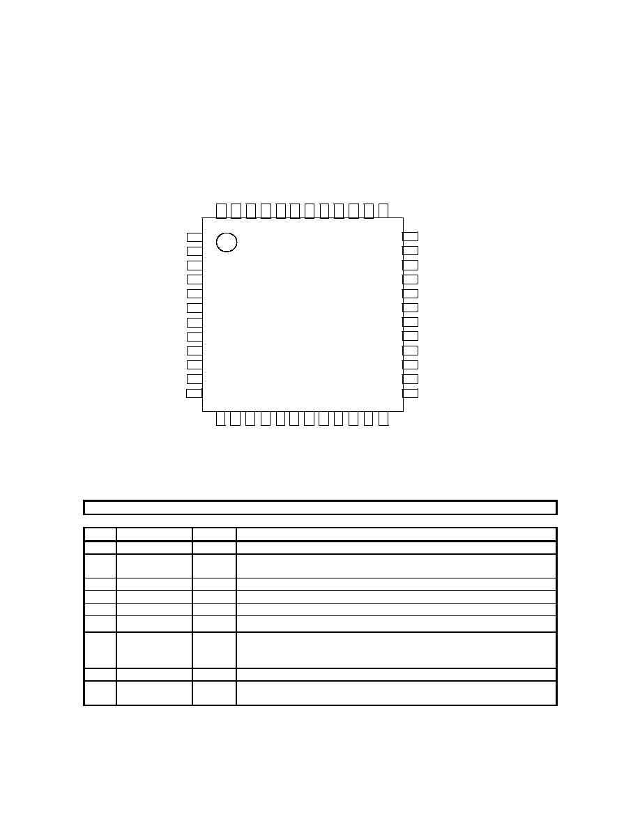
o
48pin LQFP Package
SCF
DAC
DATT
DZF
LOUT1+
LOUT1-
SCF
DAC
DATT
ROUT1+
ROUT1-
SCF
DAC
DATT
LOUT2+
LOUT2-
SCF
DAC
DATT
ROUT2+
ROUT2-
SCF
DAC
DATT
LOUT3+
LOUT3-
SCF
DAC
DATT
ROUT3+
ROUT3-
Audio
I/F
Control
Register
AK4357
MCLK
LRCK
BICK
DCLK
DSDL1
DSDR1
CSN
CCLK
CDTI
SDTI1
SDTI2
SDTI3
DSDL2
DSDR2
DSDL3
DSDR3
PCM
DSD
192kHz 24-Bit 6ch DAC with DSD Input
AK4357
ASAHI KASEI
[AK4357]
MS0088-E-02
2002/07
- 2 -
n
Ordering Guide
AK4357VQ -40
+85
∞
C 48LQFP
AKD4357 Evaluation Board for AK4357
n
Pin Layout
LOUT1-
ROUT1+
1
LOUT1+
48
2
DZFL1
3
DAFR1
4
DZF23
5
CAD0
6
CAD1
7
PDN
8
BICK
9
MCLK
10
DVDD
ROUT1-
47
LOUT2+
46
45
44
ROUT2-
43
LOUT3+
42
LOUT3-
41
ROUT3+
40
ROUT3-
39
AVSS
38
DVSS
13
SDTI1
14
SDTI2
15
SDTI3
16
LRCK
17
18
CCLK
19
CDTI
20
CSN
21
DSDM
22
DCLK
23
36
35
34
33
32
31
30
29
28
27
26
AVSS
AVDD
VREFH
DIF2
DIF1
DIF0
DSDR3
DSDL3
DSDR2
DSDL2
DSDR1
AK4357VQ
Top View
SMUTE
LOUT2-
ROUT2+
AVSS
37
NC
24
11
NC
12
25
DSDL1
PIN/FUNCTION
No.
Pin Name
I/O
Function
1
LOUT1-
O
DAC1 Lch Negative Analog Output Pin
2
LOUT1+
O
DAC1 Lch Positive Analog Output Pin
3
DZFL1
O
DAC1 Lch Zero Input Detect Pin
4
DZFR1
O
DAC1 Rch Zero Input Detect Pin
5
DZF23
O
DAC2,3 Zero Input Detect Pin
6
CAD0
I
Chip Address 0 Pin
7
CAD1
I
Chip Address 1 Pin
8
PDN
I
Power-Down Mode Pin
When at "L", the AK4357 is in the power-down mode and is held in reset.
The AK4357 should always be reset upon power-up.
9
BICK
I
Audio Serial Data Clock Pin
10
MCLK
I
Master Clock Input Pin
An external TTL clock should be input on this pin.
ASAHI KASEI
[AK4357]
MS0088-E-02
2002/07
- 3 -
No.
Pin Name
I/O
Function
11
DVDD
-
Digital Power Supply Pin, +4.75
+5.25V
12
NC
-
NC pin
No internal bonding
13
DVSS
-
Digital Ground Pin
14
SDTI1
I
DAC1 Audio Serial Data Input Pin
15
SDTI2
I
DAC2 Audio Serial Data Input Pin
16
SDTI3
I
DAC3 Audio Serial Data Input Pin
17
LRCK
I
L/R Clock Pin
18
SMUTE
I
Soft Mute Pin
When this pin goes to "H", soft mute cycle is initialized.
When returning to "L", the output mute releases.
19
CCLK
I
Control Data Clock Pin
20
CDTI
I
Control Data Input Pin
21
CSN
I
Chip Select Pin
22
DSDM
I
DSD Mode Enable Pin (Pull-down Pin)
"0": PCM mode "1": DSD mode
23
DCLK
I
DSD Clock Pin
24
NC
-
NC pin
No internal bonding
25
DSDL1
I
DAC1 DSD Lch Data Input Pin
26
DSDR1
I
DAC1 DSD Rch Data Input Pin
27
DSDL2
I
DAC2 DSD Lch Data Input Pin
28
DSDR2
I
DAC2 DSD Rch Data Input Pin
29
DSDL3
I
DAC3 DSD Lch Data Input Pin
30
DSDR3
I
DAC3 DSD Rch Data Input Pin
31
DIF0
I
Audio Data Interface Format 0 Pin
32
DIF1
I
Audio Data Interface Format 1 Pin
33
DIF2
I
Audio Data Interface Format 2 Pin
34
VREFH
I
Positive Voltage Reference Input Pin
35
AVDD
-
Analog Power Supply Pin, +4.75
+5.25V
36
AVSS
-
Analog Ground Pin
37
AVSS
-
Analog Ground Pin
38
AVSS
-
Analog Ground Pin
39
ROUT3-
O
DAC3 Rch Negative Analog Output Pin
40
ROUT3+
O
DAC3 Rch Positive Analog Output Pin
41
LOUT3-
O
DAC3 Lch Negative Analog Output Pin
42
LOUT3+
O
DAC3 Lch Positive Analog Output Pin
43
ROUT2-
O
DAC2 Rch Negative Analog Output Pin
44
ROUT2+
O
DAC2 Rch Positive Analog Output Pin
45
LOUT2-
O
DAC2 Lch Negative Analog Output Pin
46
LOUT2+
O
DAC2 Lch Positive Analog Output Pin
47
ROUT1-
O
DAC1 Rch Negative Analog Output Pin
48
ROUT1+
O
DAC1 Rch Positive Analog Output Pin
Note: All input pins except pull-down pin should not be left floating.
ASAHI KASEI
[AK4357]
MS0088-E-02
2002/07
- 4 -
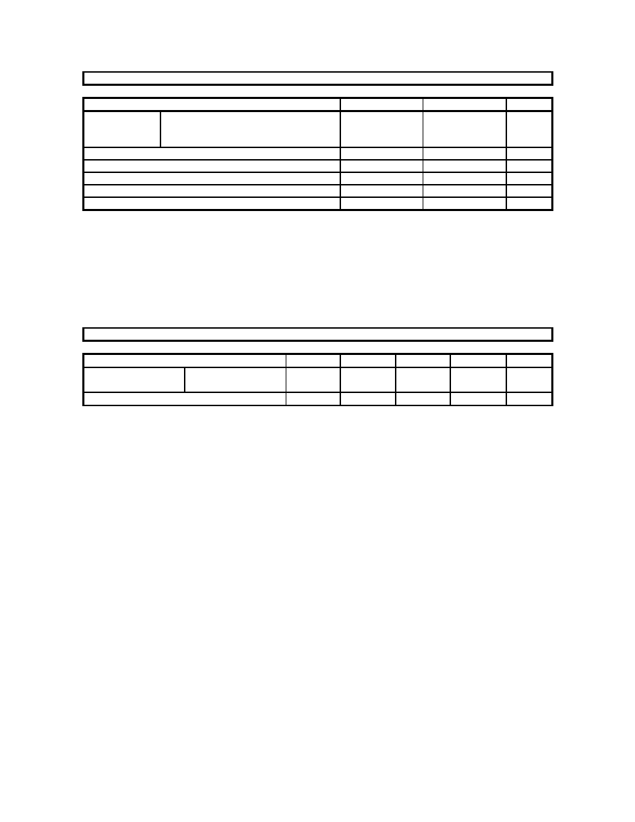
ABSOLUTE MAXIMUM RATINGS
(AVSS, DVSS=0V; Note 1)
Parameter
Symbol
min
max
Units
Power Supplies
Analog
Digital
|AVSS-DVSS| (Note 2)
AVDD
DVDD
GND
-0.3
-0.3
-
6.0
6.0
0.3
V
V
V
Input Current (any pins except for supplies)
IIN
-
±
10
mA
Analog Input Voltage
VINA
-0.3
AVDD+0.3
V
Digital Input Voltage
VIND
-0.3
DVDD+0.3
V
Ambient Operating Temperature
Ta
-40
85
∞
C
Storage Temperature
Tstg
-65
150
∞
C
Note: 1. All voltages with respect to ground.
2. AVSS and DVSS must be connected to the same analog ground plane.
WARNING: Operation at or beyond these limits may result in permanent damage to the device.
Normal operation is not guaranteed at these extremes.
RECOMMENDED OPERATING CONDITIONS
(AVSS, DVSS=0V; Note 1)
Parameter
Symbol
min
typ
max
Units
Power Supplies
(Note 3)
Analog
Digital
AVDD
DVDD
4.75
4.75
5.0
5.0
5.25
5.25
V
V
Voltage Reference
VREF
AVDD-0.5
-
AVDD
V
Note: 1. All voltages with respect to ground.
3. The power up sequence between AVDD and DVDD is not critical.
*AKM assumes no responsibility for the usage beyond the conditions in this datasheet.

ASAHI KASEI
[AK4357]
MS0088-E-02
2002/07
- 5 -
ANALOG CHARACTERISTICS
(Ta=25
∞
C; AVDD, DVDD=5V; VREF=AVDD; fs=44.1kHz; BICK=64fs; Signal Frequency=1kHz; 24bit Input Data;
Measurement frequency=20Hz
20kHz; R
L
4k
; unless otherwise specified)
Parameter
min
typ
max
Units
Resolution
24
Bits
Dynamic Characteristics
(Note 4)
fs=44.1kHz
BW=20kHz
0dBFS
-90
-86
dB
fs=96kHz
BW=40kHz
0dBFS
-88
-84
-
dB
dB
THD+N
fs=192kHz
BW=40kHz
0dBFS
-86
-
-
dB
dB
Dynamic Range (-60dBFS with A-weighted) (Note 5)
100
106
dB
S/N (A-weighted) (Note 6)
100
106
dB
Interchannel Isolation (1kHz)
90
100
dB
Interchannel Gain Mismatch
0.2
0.5
dB
DC Accuracy
Gain Drift
100
-
ppm/
∞
C
Output Voltage (Note 7)
±
2.35
±
2.5
±
2.65
Vpp
Load Resistance (Note 8)
4
k
Power Supplies
Power Supply Current (AVDD+DVDD)
Normal Operation (PDN = "H", fs
96kHz)
Normal Operation (PDN = "H", fs=192kHz)
Power-Down Mode (PDN = "L") (Note 9)
50
60
10
75
85
100
mA
mA
µA
Note: 4. Measured by Audio Precision System Two. Refer to the evaluation board manual.
5. 100dB at 16bit data.
6. S/N is independent of input bit length.
7. Full scale voltage (0dB). Output voltage scales with the voltage of VREFH pin.
AOUT(typ.@0dB)=(AOUT+)-(AOUT-)=
±
2.5Vpp*VREFH/5.0
8. For AC-load. 8k
for DC-load
9. All digital inputs including clock pins (MCLK, BICK and LRCK) are held DVDD or DVSS.