 | –≠–ª–µ–∫—Ç—Ä–æ–Ω–Ω—ã–π –∫–æ–º–ø–æ–Ω–µ–Ω—Ç: AK4394VF | –°–∫–∞—á–∞—Ç—å:  PDF PDF  ZIP ZIP |
ASAHI KASEI
[AK4394]
M0081-E-00
1999/11
- 1 -
GENERAL DESCRIPTION
The AK4394 is a high performance stereo DAC for the 192kHz sampling mode of DVD-Audio including a
24bit digital filter. The AK4394 introduces the advanced multi-bit system for
DS
modulator. This new
architecture achieves the wider dynamic range, while keeping much the same superior distortion
characteristics as conventional Single-Bit way. In the AK4394, the analog outputs are filtered in the
analog domain by switched-capacitor filter(SCF) with high tolerance to clock jitter. The analog outputs
are full differential output, so the device is suitable for hi-end applications. The digital I/F can correspond
to TTL levels, so it is easy to I/F with 3.3V logic IC.
FEATURES
∑
128x Oversampling
∑
Sampling Rate up to 192kHz
∑
24Bit 8x Digital Filter (Slow-roll-off option)
Ripple:
±
0.005dB, Attenuation: 75dB
∑
High Tolerance to Clock Jitter
∑
Low Distortion Differential Output
∑
Digital de-emphasis for 32, 44.1, 48 & 96kHz sampling
∑
Soft Mute
∑
THD+N: -100dB
∑
DR, S/N: 120dB
∑
I/F format :
MSB justified, 16/20/24bit LSB justified, I
2
S
∑
Master Clock:
Normal Speed: 256fs, 384fs, 512fs or 768fs
Double Speed: 128fs, 192fs, 256fs or 384fs
Quad Speed: 128fs or 192fs
∑
Power Supply: 5V±5%
∑
TTL Level Digital I/F
∑
Small Package: 28pin VSOP
∑
Pin Compatible with AK4393
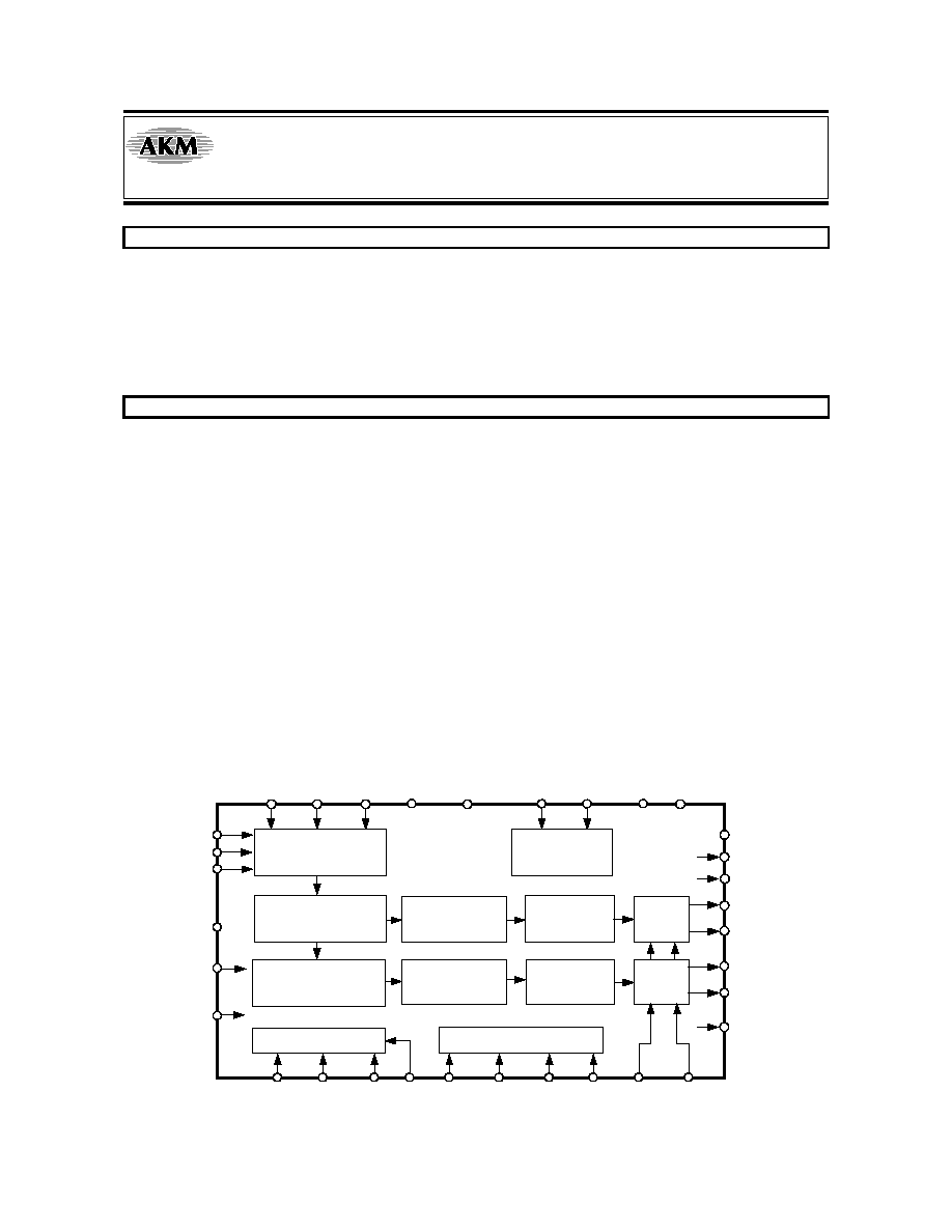
DEM1
LRCK
BICK
SDATA
Audio Data
Interface
DEM0
DVDD
CSN
AVDD
AOUTR+
8x
Interpolator
SCF
DS
Modulator
AOUTR-
SCF
De-emphasis
Soft Mute
Control Register
Clock Divider
De-emphasis
Control
PDN
CCLK
CDTI
P/S
MCLK
CKS0
CKS1
CKS2 VREFH VREFL
AOUTL+
AOUTL-
VCOM
BVSS
AVSS
DVSS
DIF2
DIF1
DIF0
SMUTE
DFS0
DZFL
DZFR
De-emphasis
Soft Mute
8x
Interpolator
DS
Modulator
Advanced Multi-Bit 192kHz 24-Bit
DS
DAC
AK4394

ASAHI KASEI
[AK4394]
M0081-E-00
1999/11
- 2 -
n
Ordering Guide
AK4394VF
-40 ~ +85
∞C
28pin VSOP (0.65mm pitch)
AKD4394
Evaluation Board
n
n
n
n
Pin Layout
6
5
4
3
2
1
DVSS
DVDD
PDN
MCLK
BICK
SDATA
LRCK
7
SMUTE/CSN
8
CKS2/DZFR
CKS1
CKS0/DZFL
P/S
VCOM
AOUTL
+
AOUTL-
AOUTR+
Top
View
10
9
DFS0
DEM0/CCLK
DEM1/CDTI
11
DIF0
12
AOUTR-
AVSS
AVDD
VREFH
23
24
25
26
27
28
22
21
19
20
18
17
13
14
16
15
DIF1
DIF2
VREFL
BVSS
n
n
n
n
Pin Compatibility with AK4393
AK4393
AK4394
fs (max)
108kHz
216kHz
slow roll-off filter
not available
available
zero detection
not available
available
DVDD
3~5.25V
4.75~5.25V
pin #26 (serial mode)
CKS0
DZFL
pin #28 (serial mode)
CKS2
DZFR
Control register : 01H D4
0
DFS1
Control register : 01H D5
0
SLOW
Control register : 01H D6
0
DZFM
Control register : 01H D7
0
DZFE

ASAHI KASEI
[AK4394]
M0081-E-00
1999/11
- 3 -
PIN/FUNCTION
No.
Pin Name
I/O
Function
1
DVSS
-
Digital Ground Pin
2
DVDD
-
Digital Power Supply Pin, 5.0V
3
MCLK
I
Master Clock Input Pin
4
PDN
I
Power-Down Mode Pin
When at "L", the AK4394 is in power-down mode and is held in reset.
The AK4394 should always be reset upon power-up.
5
BICK
I
Audio Serial Data Clock Pin
The clock of 64fs or more than is recommended to be input on this pin.
6
SDATA
I
Audio Serial Data Input Pin
2's complement MSB-first data is input on this pin.
7
LRCK
I
L/R Clock Pin
SMUTE
I
Soft Mute Pin in parallel mode
When this pin goes "H", soft mute cycle is initiated.
When returning "L", the output mute releases.
8
CSN
I
Chip Select Pin in serial mode
9
DFS0
I
Double Speed Sampling Mode Pin (Internal pull-down pin)
"L": Normal Speed , "H": Double Speed
DEM0
I
De-emphasis Enable Pin in parallel mode
10
CCLK
I
Control Data Clock Pin in serial mode
DEM1
I
De-emphasis Enable Pin in parallel mode
11
CDTI
I
Control Data Input Pin in serial mode
12
DIF0
I
Digital Input Format Pin
13
DIF1
I
Digital Input Format Pin
14
DIF2
I
Digital Input Format Pin
15
BVSS
-
Substrate Ground Pin, 0V
16
VREFL
I
Low Level Voltage Reference Input Pin
17
VREFH
I
High Level Voltage Reference Input Pin
18
AVDD
-
Analog Power Supply Pin, 5.0V
19
AVSS
-
Analog Ground Pin, 0V
20
AOUTR-
O
Rch Negative analog output Pin
21
AOUTR+
O
Rch Positive analog output Pin
22
AOUTL-
O
Lch Negative analog output Pin
23
AOUTL+
O
Lch Positive analog output Pin
24
VCOM
O
Common Voltage Output Pin, 2.6V
25
P/S
I
Parallel/Serial Select Pin (Internal pull-up pin)
"L": Serial control mode, "H": Parallel control mode
CKS0
I
Master Clock Select Pin in parallel mode
26
DZFL
O
Lch Zero Input Detect Pin in serial mode
27
CKS1
I
Master Clock Select Pin
CKS2
I
Master Clock Select Pin in parallel mode
28
DZFR
O
Rch Zero Input Detect Pin in serial mode
Note: All input pins except internal pull-up/down pins should not be left floating.

ASAHI KASEI
[AK4394]
M0081-E-00
1999/11
- 4 -
ABSOLUTE MAXIMUM RATINGS
(AVSS, BVSS, DVSS = 0V; Note 1)
Parameter
Symbol
min
max
Units
Power Supplies:
Analog
Digital
| BVSS-DVSS | (Note 2)
AVDD
DVDD
D GND
-0.3
-0.3
-
6.0
6.0
0.3
V
V
V
Input Current , Any pin Except Supplies
IIN
-
±10
mA
Input Voltage
VIND
-0.3
DVDD+0.3
V
Ambient Operating Temperature
Ta
-40
85
∞C
Storage Temperature
Tstg
-65
150
∞C
Notes: 1. All voltages with respect to ground.
2. AVSS, BVSS and DVSS must be connected to the same analog ground plane.
WARNING: Operation at or beyond these limits may result in permanent damage to the device.
Normal operation is not guaranteed at these extremes.
RECOMMENDED OPERATING CONDITIONS
(AVSS, BVSS, DVSS=0V; Note 1)
Parameter
Symbol
min
typ
max
Units
Power Supplies:
(Note 3)
Analog
Digital
AVDD
DVDD
4.75
4.75
5.0
5.0
5.25
5.25
V
V
Voltage Reference
(Note 4)
"H" voltage reference
"L" voltage reference
VREFH-VREFL
VREFH
VREFL
D VREF
AVDD-0.5
AVSS
3.0
-
-
-
AVDD
-
AVDD
V
V
V
Notes: 3. The power up sequence between AVDD and DVDD is not critical.
4. Analog output voltage scales with the voltage of (VREFH-VREFL).
AOUT (typ.@0dB) = (AOUT+) - (AOUT-) =
±2.4Vpp◊(VREFH-VREFL)/5.
* AKM assumes no responsibility for the usage beyond the conditions in this data sheet.

ASAHI KASEI
[AK4394]
M0081-E-00
1999/11
- 5 -
ANALOG CHARACTERISTICS
(Ta = 25
∞C; AVDD, DVDD = 5V; AVSS, BVSS, DVSS = 0V, VREFH = AVDD, VREFL = AVSS;
fs = 44.1kHz; BICK = 64fs; Signal Frequency = 1kHz; 24bit Input Data; Measurement Bandwidth = 20Hz~20kHz;
R
L
≥ 600W; External circuit: Figure 12; unless otherwise specified)
Parameter
min
typ
max
Units
Resolution
24
Bits
Dynamic Characteristics (Note 5)
fs=44.1kHz
BW=20kHz
0dBFS
-60dBFS
-100
-53
-90
-
dB
dB
fs=96kHz
BW=40kHz
0dBFS
-60dBFS
-97
-51
-87
-
dB
dB
THD+N
fs=192kHz
BW=40kHz
0dBFS
-60dBFS
-97
-51
-
-
dB
dB
Dynamic Range (-60dBFS with A-weighted) (Note 6)
(Note 7)
112
-
117
120
dB
dB
S/N (A-weighted (Note 8)
(Note 7)
112
-
117
120
dB
dB
Interchannel Isolation (1kHz)
100
120
dB
DC Accuracy
Interchannel Gain Mismatch
0.15
0.3
dB
Gain Drift (Note 9)
20
-
ppm/
∞C
Output Voltage (Note 10)
±2.25
±2.4
±2.55
Vpp
Load Resistance (Note 11)
600
W
Output Current
3.5
mA
Power Supplies
Power Supply Current
Normal Operation (PDN = "H")
AVDD
DVDD(fs=44.1kHz)
DVDD(fs=96kHz)
DVDD(fs=192kHz)
AVDD + DVDD
60
5
8
12
-
-
-
-
90
mA
mA
mA
mA
mA
Power-Down Mode (PDN = "L")
AVDD + DVDD (Note 12)
10
100
µA
Power Supply Rejection (Note 13)
50
dB
Notes: 5. At 44.1kHz, measured by Audio Precision, System Two. Averaging mode.
At 96kHz and 192kHz, measured by ROHDE & SCHWARZ, UPD. Averaging mode.
Refer to the eva board manual.
6. 101dB at 16bit data and 116dB at 20bit data.
7. By Figure13. External LPF Circuit Example 2.
8. S/N does not depend on input bit length.
9. The voltage on (VREFH-VREFL) is held +5V externally.
10. Full-scale voltage(0dB). Output voltage scales with the voltage of (VREFH-VREFL).
AOUT (typ.@0dB) = (AOUT+) - (AOUT-) =
±2.4Vpp◊(VREFH-VREFL)/5.
11. For AC-load. 1k
W for DC-load.
12. In the power-down mode. P/S = DVDD, and all other digital input pins including clock pins (MCLK, BICK and
LRCK) are held DVSS.
13. PSR is applied to AVDD, DVDD with 1kHz, 100mVpp. VREFH pin is held +5V.