
ASAHI KASEI
[AK4529]
MS0082-E-00
2001/3
- 1 -
GENERAL DESCRIPTION
The AK4529 is a single chip CODEC that includes two channels of ADC and eight channels of DAC. The
ADC outputs 24bit data and the DAC accepts up to 24bit input data. The ADC has the Enhanced Dual Bit
architecture with wide dynamic range. The DAC introduces the new developed Advanced Multi-Bit
architecture, and achieves wider dynamic range and lower outband noise. An auxiliary digital audio input
interface maybe used instead of the ADC for passing audio data to the primary audio output port. Control
may be set directly by pins or programmed through a separate serial interface.
The AK4529 has a dynamic range of 102dB for ADC, 106dB for DAC and is well suited for digital surround
for home theater and car audio. An AC-3 system can be built with a IEC60958(SPDIF) receiver such as
the AK4112A. The AK4529 is available in a small 44pin LQFP package which will reduce system space.
*AC-3 is a trademark of Dolby Laboratories.
FEATURES
o
2ch 24bit ADC
- 64x Oversampling
- Sampling Rate up to 96kHz
- Linear Phase Digital Anti-Alias Filter
- Single-Ended Input
- S/(N+D): 92dB
- Dynamic Range, S/N: 102dB
- Digital HPF for offset cancellation
- I/F format: MSB justified, I
2
S or TDM
- Overflow flag
o
8ch 24bit DAC
- 128x Oversampling
- Sampling Rate up to 96kHz
- 24bit 8 times Digital Filter
- Single-Ended Outputs
- On-chip Switched-Capacitor Filter
- S/(N+D): 90dB
- Dynamic Range, S/N: 106dB
- I/F format: MSB justified, LSB justified(20bit,24bit), I
2
S or TDM
- Individual channel digital volume with 256 levels and 0.5dB step
- Soft mute
- De-emphasis for 32kHz, 44.1kHz and 48kHz
- Zero Detect Function
o
High Jitter Tolerance
o
TTL Level Digital I/F
o
3-wire Serial and I
2
C Bus �P I/F for mode setting
o
Master clock:256fs, 384fs or 512fs for fs=32kHz to 48kHz
128fs, 192fs or 256fs for fs=64kHz to 96kHz
o
Power Supply: 4.5 to 5.5V
o
Power Supply for output buffer: 2.7 to 5.5V
o
Small 44pin LQFP
High Performance Multi-channel Audio CODEC
AK4529
ASAHI KASEI
[AK4529]
MS0082-E-00
2001/3
- 2 -
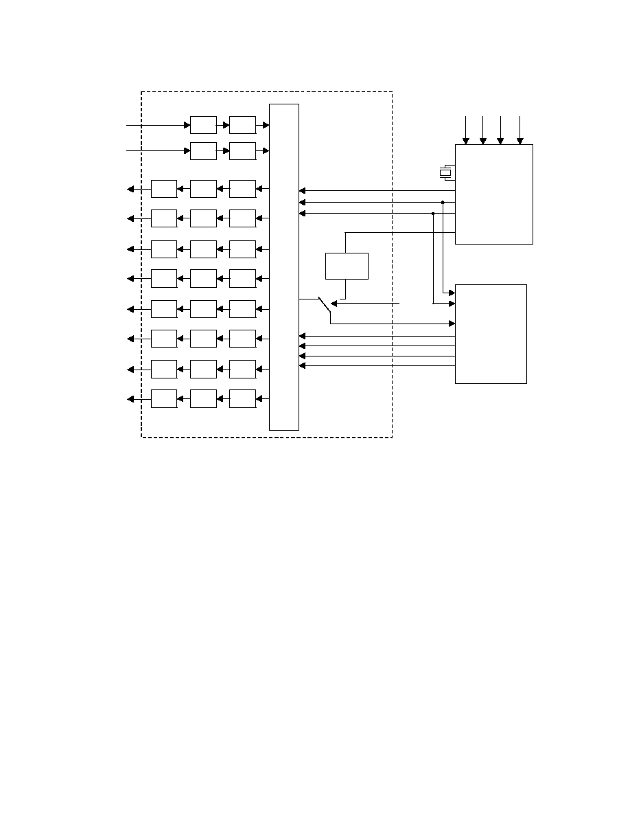
n
Block Diagram
Audio
I/F
LPF
LPF
DAC
DATT
LPF
DAC
DATT
LPF
DAC
DATT
LPF
DAC
DATT
LPF
DAC
DATT
LOUT1
ROUT1
LOUT2
ROUT2
LOUT3
ROUT3
DAC
DATT
AK4529
ADC
HPF
ADC
HPF
RIN
LIN
LRCK
BICK
SDOUT1
SDOUT2
SDOUT3
AC3
SDIN
MCKO
LRCK
BICK
XTI
XTO
DIR
SDTO
AK4112A
RX4
RX3
RX2
RX1
LRCK
BICK
SDTI1
SDTI2
SDTI3
DAUX
SDOS
MCLK
LRCK
BICK
SDOUT
SDIN1
SDIN2
SDIN3
MCLK
SDTO
Format
Converter
SDOUT4
SDTI4
SDIN4
LPF
DAC
DATT
LPF
DAC
DATT
LOUT4
ROUT4
Block Diagram (DIR and AC-3 DSP are external parts)
ASAHI KASEI
[AK4529]
MS0082-E-00
2001/3
- 3 -
n
Ordering Guide
AK4529VQ
-40
+85
�
C
44pin LQFP(0.8mm pitch)
AKD4529
Evaluation Board for AK4529
n
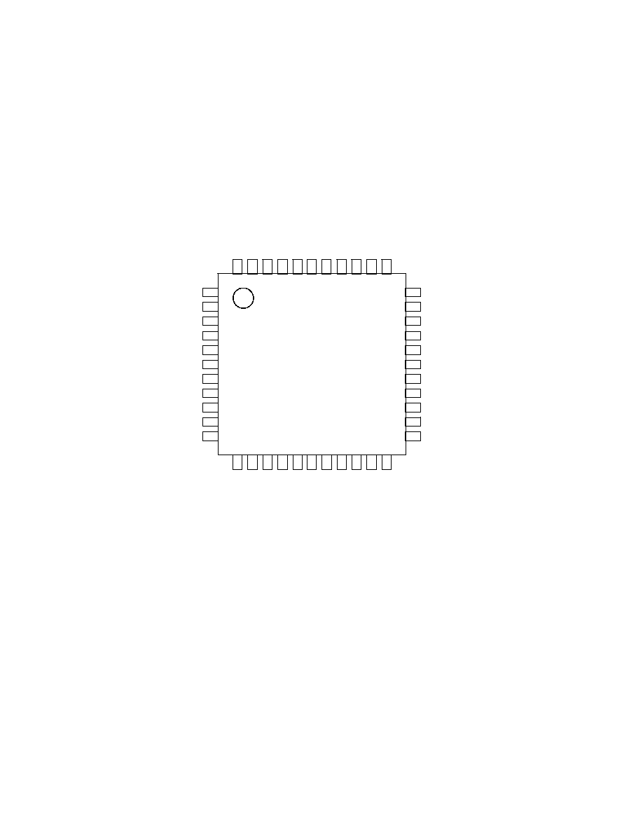
Pin Layout
SDOS
TDM
1
I2C
4
4
2
SMUTE
3
BICK
4
LRCK
5
SDTI1
6
SDTI2
7
SDTI3
8
SDTO
9
DAUX
10
DFS
11
LOOP0/SDA/CDTI
4
3
DIF1/SCL/CCLK
42
41
4
0
MCLK
3
9
DZF1
3
8
AVSS
37
AVDD
3
6
VREFH
3
5
VCOM
3
4
SDTI4
12
DZFE
13
TVDD
14
DVDD
15
DVSS
16
17
TST
18
CAD1
19
CAD0
20
LOUT4
21
ROUT4
22
33
32
31
30
29
28
27
26
25
24
23
DZF2/OVF
RIN
LIN
NC
NC
ROUT1
LOUT1
ROUT2
LOUT2
ROUT3
LOUT3
AK4529VQ
Top View
PDN
DIF0/CSN
P/S

ASAHI KASEI
[AK4529]
MS0082-E-00
2001/3
- 4 -
n
Compatibility with AK4527B
1. Functions
Functions
AK4527B
AK4529
DAC channel
6ch
8ch
ADC
Full-differential input
(with single-ended use capability)
Single-ended input
DATT transition time
7424/fs (fixed)
7424/fs, 1024/fs or 256/fs
I
2
C bus auto increment
Not available
Available
TDM I/F format
Not available
Available
2. Pin Configuration
pin#
AK4527
AK4529
12
NC
SDTI4
19
NC
CAD1
20
NC
CAD0
21
CAD1
LOUT4
22
CAD0
ROUT4
29
LIN-
NC
30
LIN+
NC
31
RIN-
LIN
32
RIN+
RIN
44
LOOP1
TDM
3. Register
Addr
Changed items
00H
TDM (TDM I/F format mode) is added.
08H
DEMD1-0 (DAC4 De-emphasis) are added.
09H
ATS1-0 (DATT transition time) are added.
0AH
DZFM3 (Zero detection mode) is added.
0BH
ATT7-0 (LOUT4 output volume control) are added.
0CH
ATT7-0 (ROUT4 output volume control) are added.
ASAHI KASEI
[AK4529]
MS0082-E-00
2001/3
- 5 -
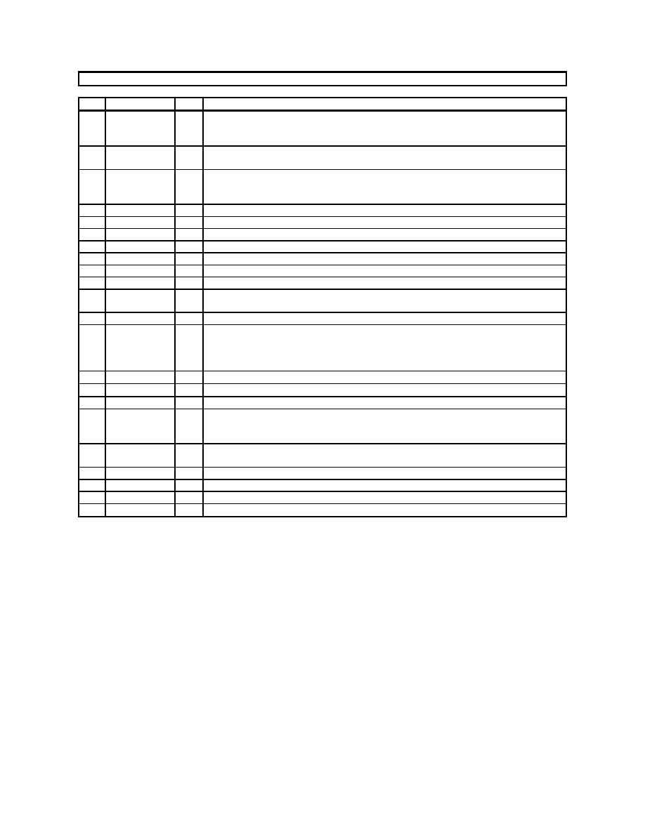
PIN/FUNCTION
No.
Pin Name
I/O
Function
1
SDOS
I
SDTO Source Select Pin (Note 1)
"L": Internal ADC output, "H": DAUX input
SDOS pin should be set to "L" when TDM= "1".
2
I2C
I
Control Mode Select Pin
"L": 3-wire Serial, "H": I
2
C Bus
3
SMUTE
I
Soft Mute Pin (Note 1)
When this pin goes to "H", soft mute cycle is initialized.
When returning to "L", the output mute releases.
4
BICK
I
Audio Serial Data Clock Pin
5
LRCK
I
Input Channel Clock Pin
6
SDTI1
I
DAC1 Audio Serial Data Input Pin
7
SDTI2
I
DAC2 Audio Serial Data Input Pin
8
SDTI3
I
DAC3 Audio Serial Data Input Pin
9
SDTO
O
Audio Serial Data Output Pin
10
DAUX
I
AUX Audio Serial Data Input Pin
11
DFS
I
Double Speed Sampling Mode Pin (Note 1)
"L": Normal Speed, "H": Double Speed
12
SDTI4
I
DAC4 Audio Serial Data Input Pin
13
DZFE
I
Zero Input Detect Enable Pin
"L": mode 7 (disable) at parallel mode,
zero detect mode is selectable by DZFM3-0 bits at serial mode
"H": mode 0 (DZF1 is AND of all eight channels)
14
TVDD
-
Output Buffer Power Supply Pin, 2.7V
5.5V
15
DVDD
-
Digital Power Supply Pin, 4.5V
5.5V
16
DVSS
-
Digital Ground Pin, 0V
17
PDN
I
Power-Down & Reset Pin
When "L", the AK4529 is powered-down and the control registers are reset to default
state. If the state of P/S or CAD0-1 changes, then the AK4529 must be reset by PDN.
18
TST
I
Test Pin
This pin should be connected to DVSS.
19
CAD1
I
Chip Address 1 Pin
20
CAD0
I
Chip Address 0 Pin
21
LOUT4
O
DAC4 Lch Analog Output Pin
22
ROUT4
O
DAC4 Rch Analog Output Pin