 | –≠–ª–µ–∫—Ç—Ä–æ–Ω–Ω—ã–π –∫–æ–º–ø–æ–Ω–µ–Ω—Ç: AK5355VT | –°–∫–∞—á–∞—Ç—å:  PDF PDF  ZIP ZIP |
ASAHI KASEI
[AK5355]
MS0113-E-00
2001/08
- 1 -
FEATURES
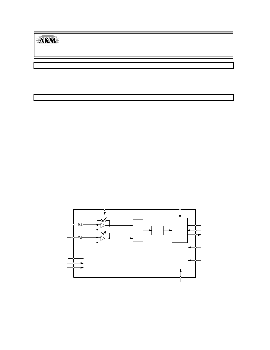
The AK5355 is a low voltage 16bit A/D converter for digital audio systems. The AK5355 also includes an
Input Gain Amplifier, making it suitable for microphone applications or low-input signal levels. The analog
signal input of the AK5355 is single-ended, eliminating the need for external filters. The AK5355 is
housed in a space-saving 16-pin TSSOP package.
FEATURES
1. Resolution: 16bits
2. Recording Functions
∑
Gain Amplifier (0dB / +15dB)
∑
Digital HPF for DC-offset cancellation (fc=3.4Hz@fs=44.1kHz)
3. ADC Characteristics
∑
Single-ended Input
∑
Input Level: 1.8Vpp@VA=3.0V (= 0.6 x VA)
∑
S/(N+D): 85dB
∑
DR, S/N: 91dB
4. Master Clock: 256fs/384fs/512fs
5. Audio Data Format: MSB First, 2's compliment
∑
16bit MSB justified or I
2
S
8. Power Supply
∑
VA, VD: 2.1
3.6V (typ. 3.0V)
9. Power Supply Current: 5mA
10. Ta = -40
85
∞
C
11. Package: 16pin TSSOP
LIN
VCOM
VA
VSS
MCLK
SDTO
BCLK
LRCK
VD
ADC
HPF
Audio I/F
Controller
Clock Divider
PDN
RIN
DIF
SEL
Low Power 16bit
ADC
AK5355
ASAHI KASEI
[AK5355]
MS0113-E-00
2001/08
- 2 -
Ordering Guide
AK5355VT
-40
+85
∞
C
16pin TSSOP (0.65mm pitch)
AKD5355
Evaluation Board for AK5355
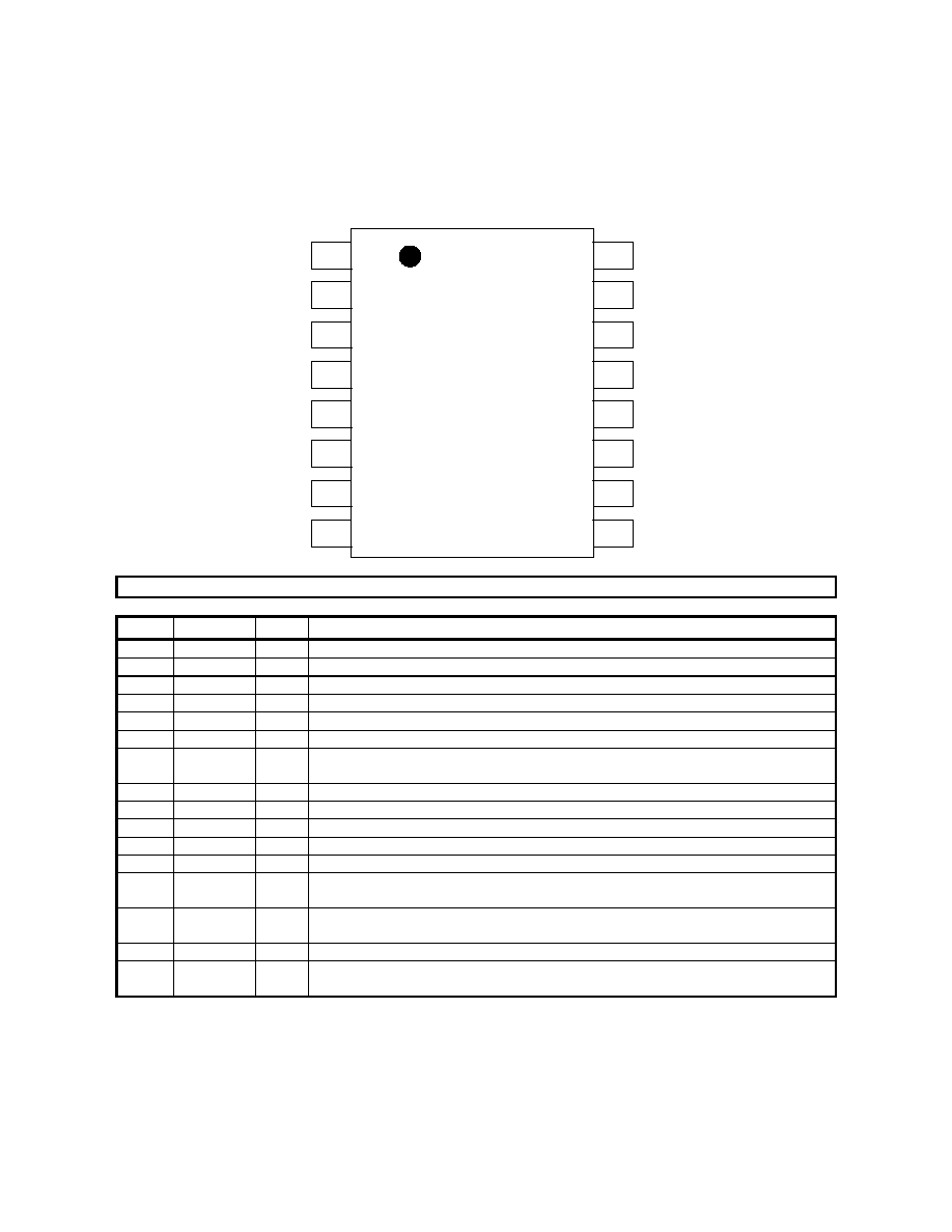
Pin Layout
1
VCOM
RIN
VSS
LIN
VA
VD
SEL
NC
Top
View
2
3
4
5
6
7
8
TST1
NC
BCLK
MCLK
LRCK
SDTO
16
15
14
13
12
11
10
9
DIF
PDN
PIN/FUNCTION
No.
Pin Name
I/O
Function
1
VCOM
O
ADC Common Voltage Output Pin
2
RIN
I
Rch Input Pin
3
LIN
I
Lch Input Pin
4
VSS
-
Ground Pin
5
VA
-
Analog Power Supply Pin, +3.0V
6
VD
-
Digital Power Supply Pin, +3.0V
7
SEL
I
Input Gain Select Pin
"L": 0dB, "H": +15dB
8
NC
-
NC Pin (No internal bonding)
9
SDTO
O
Audio Serial Data Output Pin
10
LRCK
I
Input/Output Channel Clock Pin
11
MCLK
I
Master Clock Input Pin
12
BCLK
I
Audio Serial Data Clock Pin
13
PDN
I
Reset & Power Down Pin
"L" : Reset & Power down, "H" : Normal operation
14
DIF
I
Audio Data Format Select Pin
"L": MSB justified, "H": I
2
S
15
NC
-
NC Pin (No internal bonding)
16
TST1
I
TEST pin (Pull-down Pin)
This pin should be left floating or connected to VSS
Note: All digital input pins should not be left floating.

ASAHI KASEI
[AK5355]
MS0113-E-00
2001/08
- 3 -
ABSOLUTE MAXIMUM RATINGS
(VSS=0V; Note 1)
Parameter
Symbol
Min
max
Units
Power Supply
Analog
Digital
VA
VD
-0.3
-0.3
4.6
4.6
V
V
Input Current (Any Pin Except Supplies)
IIN
-
±
10
mA
Analog Input Voltage (LIN, RIN pins)
VINA
-0.3
VA+0.3
V
Digital Input Voltage
VIND
-0.3
VD+0.3
V
Ambient Temperature (power applied)
Ta
-40
85
∞
C
Storage Temperature
Tstg
-65
150
∞
C
Note 1. All voltages with respect to ground.
WARNING: Operation at or beyond these limits may results in permanent damage to the device.
Normal operation is not guaranteed at these extremes.
RECOMMENDED OPERATING CONDITIONS
(VSS=0V; Note 1)
Parameter
Symbol
min
typ
max
Units
Power Supply
Analog (VA pin)
Digital (VD pin)
VA
VD
2.1
2.1
3.0
3.0
3.6
VA
V
V
Note 1. All voltages with respect to ground.
WARNING: AKM assumes no responsibility for the usage beyond the conditions in this data sheet.

ASAHI KASEI
[AK5355]
MS0113-E-00
2001/08
- 4 -
ANALOG CHARACTERISTICS
(Ta=25
∞
C; VA, VD=3.0V; fs=44.1kHz; Signal Frequency=1kHz; Measurement frequency=10Hz
20kHz;
unless otherwise specified)
Parameter
min
typ
max
Units
Resolution
16
bits
Input PGA Characteristics (IPGA):
Gain = 0dB
1.65
1.8
1.95
Vpp
Input Voltage (Note 2)
Gain = +15dB
0.29
0.32
0.35
Vpp
Gain = 0dB
27
40
k
Input Impedance
Gain = +15dB
20
30
k
ADC Analog Input Characteristics: (Note 3)
Gain = 0dB
75
85
dB
S/(N+D) (-0.5dBFS Output)
Gain = +15dB
70
80
dB
Gain = 0dB
84
91
dB
D-Range (-60dBFS Output, A-weight)
Gain = +15dB
76
84
dB
Gain = 0dB
84
91
dB
S/N (A-weight)
Gain = +15dB
76
84
dB
Gain = 0dB
90
100
dB
Interchannel Isolation
Gain = +15dB
80
90
dB
Gain = 0dB
0.2
0.5
dB
Interchannel Gain Mismatch
Gain = +15dB
0.2
1.0
dB
Power Supplies
Power Supply Current: VA+VD
Normal Operation (PDN="H")
Power Down (PDN="L") (Note 4)
5
10
7.5
100
mA
µ
A
Note 2. Analog input voltage (full-scale voltage) scales with VA.
Gain = 0dB; 0.6 x VA
Gain = +15dB; 0.107 x VA
Note 3. ADC measurements are input from LIN/RIN and routed through input gain amplifier.
The internal HPF cancels the offset of input gain amplifier and ADC.
Note 4. In case of power-down mode, all digital input pins including clocks pins (MCLK, BCLK and LRCK) are held at
VD or VSS. PDN pin is held at VSS.

ASAHI KASEI
[AK5355]
MS0113-E-00
2001/08
- 5 -
FILTER CHARACTERISTICS
(Ta=25
∞
C; VA, VD=2.1
3.6V; fs=44.1kHz)
Parameter
Symbol
min
typ
max
Units
ADC Digital Filter (Decimation LPF):
Passband (Note 5)
±
0.1dB
-1.0dB
-3.0dB
PB
0
20.0
21.1
17.4
kHz
kHz
kHz
Stopband (Note 5)
SB
27.0
kHz
Passband Ripple
PR
±
0.1
dB
Stopband Attenuation
SA
65
dB
Group Delay (Note 6)
GD
17.0
1/fs
Group Delay Distortion
GD
0
µ
s
ADC Digital Filter (HPF):
Frequency Response (Note 5)
-3dB
-0.5dB
-0.1dB
FR
3.4
10
22
Hz
Hz
Hz
Note 5. The passband and stopband frequencies scale with fs (sampling frequency).
For examples, PB=0.454 x fs(@ADC: -1.0dB).
Note 6. The calculated delay time caused by digital filtering. This time is from the input of an analog signal to setting the
16bit data of both channels to the output register of the ADC and includes the group delay of the HPF.
DC CHARACTERISTICS
(Ta=25
∞
C; VA, VD=2.1
3.6V)
Parameter
Symbol
min
typ
max
Units
High-Level Input Voltage (Except for TST1 pin)
Low-Level Input Voltage (Except for TST1 pin)
VIH
VIL
75
%
VD
-
-
-
-
25
%
VD
V
V
High-Level Output Voltage (Iout=-80
µ
A)
Low-Level Output Voltage (Iout=80
µ
A)
VOH
VOL
VD-0.4
-
-
-
0.4
V
V
Input Leakage Current (Note 7)
Iin
-
-
±
10
µ
A
Note 7. TST1 pin is pulled-down internally (typ. 100k
)