 | –≠–ª–µ–∫—Ç—Ä–æ–Ω–Ω—ã–π –∫–æ–º–ø–æ–Ω–µ–Ω—Ç: AK5384VF | –°–∫–∞—á–∞—Ç—å:  PDF PDF  ZIP ZIP |
ASAHI KASEI
[AK5384]
MS0225-E-00
2003/05
- 1 -
GENERAL DESCRIPTION
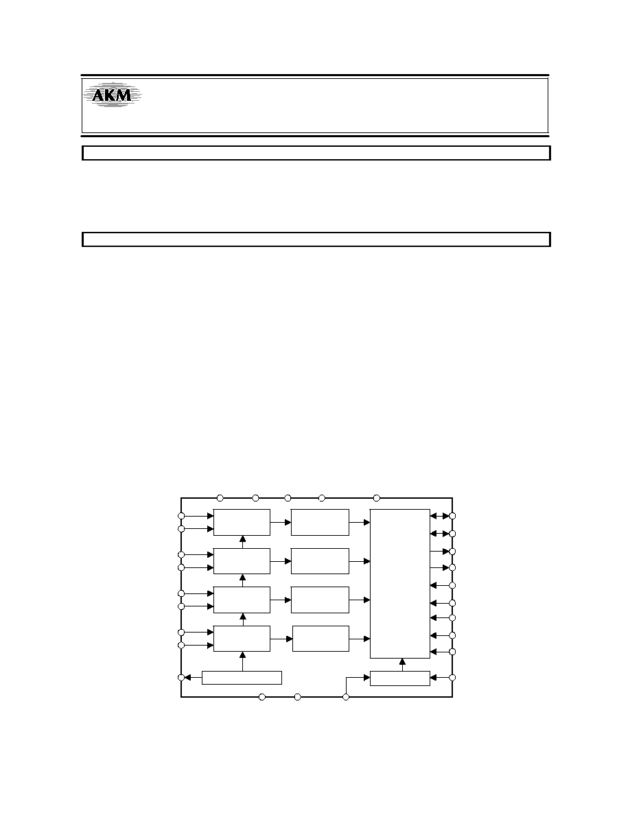
The AK5384 is a 4-channel A/D Converter with wide sampling rate of 8kHz
96kHz and is suitable for
Multi-channel audio system. The AK5384 achieves high accuracy and low cost by using Enhanced dual
bit
techniques. The AK5384 supports master mode and TDM format. Therefore, the AK5384 is
suitable for multi-channel audio system.
FEATURES
o
4-Channel
ADC
o
Differential Inputs
o
Digital HPF for DC-Offset Cancel
o
S/(N+D): 100dB@5V for 48kHz
o
DR: 107dB@5V for 48kHz
o
S/N: 107dB@5V for 48kHz
o
Sampling Rate Ranging from 8kHz to 96kHz
o
Master Clock:
256fs/384fs/512fs/768fs (
48kHz)
256fs/384fs (
96kHz)
o
TTL Digital Input Level
o
Output format: 24bit MSB justified, I
2
S or TDM
o
Cascade TDM Interface
o
Master & Slave Mode
o
Overflow Flag
o
Power Supply: 4.75 to 5.25V
o
Power Supply for output buffer: 3.0 to 5.25V
o
Ta =
-
40
85
∞
C
o
28pin VSOP
Modulator
LIN1-
LRCK
BICK
SDTO1
VCOM
Clock Divider
AVSS
AVDD
Decimation
Filter
Audio
Interface
Voltage Reference
DVSS
DVDD
PDN
LIN1+
Modulator
RIN1-
Decimation
Filter
RIN1+
Modulator
LIN2-
Decimation
Filter
LIN2+
Modulator
RIN2-
Decimation
Filter
RIN2+
SDTO2
DIF
TDM0
M/S
MCLK
CKS
TDMIN
TDM1
TVDD
OVF
107dB 24-Bit 96kHz 4-Channel ADC
AK5384
ASAHI KASEI
[AK5384]
MS0225-E-00
2003/05
- 2 -
n
Ordering Guide
AK5384VF
-
40
+85
∞
C 28pin VSOP (0.65mm pitch)
AKD5384 Evaluation Board for AK5384
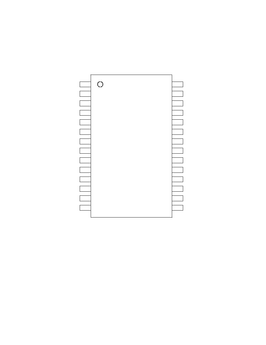
n
Pin Layout
RIN2+
RIN2-
AVSS
AVDD
LIN2+
LIN2-
TEST
VCOM
TDM1
TDM0
TDMIN
MCLK
OVF
DIF
Top View
8
7
6
5
4
3
2
1
21
22
23
24
25
26
27
28
RIN1+
RIN1-
PDN
CKS
M/S
LIN1-
LIN1+
9
10
11
12
13
14
18
19
20
TVDD
15
16
17
LRCK
BICK
SDTO2
DVDD
DVSS
SDTO1

ASAHI KASEI
[AK5384]
MS0225-E-00
2003/05
- 3 -
PIN/FUNCTION
No. Pin Name
I/O Function
1
LIN2+
I
ADC2 Lch Positive Analog Input Pin
2
LIN2
-
I
ADC2 Lch Negative Analog Input Pin
3
RIN2+
I
ADC2 Rch Positive Analog Input Pin
4
RIN2
-
I
ADC2 Rch Negative Analog Input Pin
5
TEST
I
Test Pin (Connected to AVSS)
6
VCOM
O
Common Voltage Output Pin, AVDD/2
Normally connected to AVSS with a 0.1
µ
F ceramic capacitor in parallel with an
electrolytic capacitor less than 2.2
µ
F.
7
AVSS
-
Analog Ground Pin
8
AVDD
-
Analog Power Supply Pin, 4.75
5.25V
9
DIF
I
Audio Interface Format Pin
"L" : 24bit MSB justified, "H" : 24bit I
2
S Compatible
10 TDM1
I
TDM I/F BICK Frequency Select Pin
"L" : 256fs, "H" : 128fs
11 TDM0
I
TDM I/F Format Enable Pin
"L" : Normal Mode, "H" : TDM Mode
12 TDMIN
I
TDM Data Input Pin
13 MCLK
I
Master Clock Input Pin
14 OVF
O
Analog Input Overflow Detect Pin
This pin goes to "H" if one of four analog inputs overflows.
15 LRCK
I/O
Output Channel Clock Pin
"L" Output in Master Mode at Power-down mode.
16 BICK
I/O
Audio Serial Data Clock Pin
"L" Output in Master Mode at Power-down mode.
17 SDTO2
O
ADC2 Audio Serial Data Output Pin
"L" Output at Power-down mode.
18 SDTO1
O
ADC1 Audio Serial Data Output Pin
"L" Output at Power-down mode.
19 TVDD
-
Output Buffer Power Supply Pin, 3.0
5.25V
20 DVDD
-
Digital Power Supply Pin, 4.75
5.25V
21 DVSS
-
Digital Ground Pin
22 PDN
I
Power-Down Mode Pin
When "L", the circuit is in power-down mode.
The AK5384 should always be reset upon power-up.
23 CKS
I
Master Clock Select Pin
"L" : 256fs, "H" : 512fs
This pin is enabled in Master Mode.
24 M/S
I
Master / Slave Mode Pin
"L" : Slave Mode, "H" : Master Mode
25 RIN1
-
I
ADC1 Rch Negative Analog Input Pin
26 RIN1+
I
ADC1 Rch Positive Analog Input Pin
27 LIN1
-
I
ADC1 Lch Negative Analog Input Pin
28 LIN1+
I
ADC1 Lch Positive Analog Input Pin
Note: All digital input pins should not be left floating.
ASAHI KASEI
[AK5384]
MS0225-E-00
2003/05
- 4 -
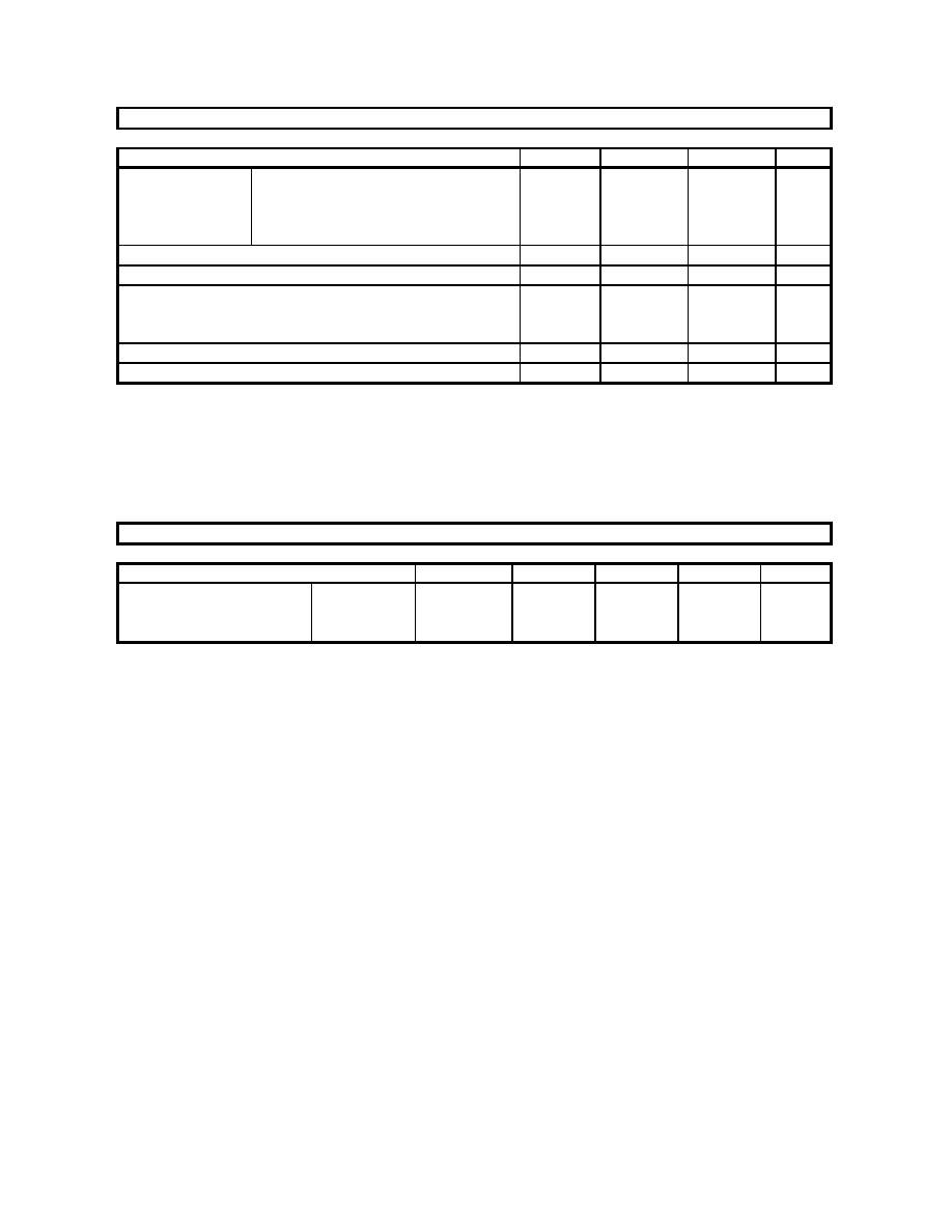
ABSOLUTE MAXIMUM RATINGS
(AVSS, DVSS=0V; Note 1)
Parameter
Symbol
min
max
Units
Power Supplies:
Analog
Digital
Output buffer
|AVSS ≠ DVSS| (Note 2)
AVDD
DVDD
TVDD
GND
-
0.3
-
0.3
-
0.3
-
6.0
6.0
6.0
0.3
V
V
V
V
Input Current, Any Pin Except Supplies
IIN
-
±
10
mA
Analog Input Voltage
VINA
-
0.3
AVDD+0.3
V
Digital Input Voltage
(Except BICK, LRCK pins)
(BICK, LRCK pins)
VIND1
VIND2
-
0.3
-
0.3
DVDD+0.3
TVDD+0.3
V
V
Ambient Temperature (Powered applied)
Ta
-
40
85
∞
C
Storage Temperature
Tstg
-
65
150
∞
C
Note 1. All voltages with respect to ground.
Note 2. AVSS and DVSS must be connected to the same analog ground plane.
WARNING: Operation at or beyond these limits may result in permanent damage to the device.
Normal operation is not guaranteed at these extremes.
RECOMMENDED OPERATING CONDITIONS
(AVSS, DVSS=0V; Note 1)
Parameter
Symbol
min
typ
max
Units
Power Supplies (Note 3)
Analog
Digital
Output buffer
AVDD
DVDD
TVDD
4.75
4.75
3.0
5.0
5.0
5.0
5.25
5.25
5.25
V
V
V
Note 1. All voltages with respect to ground.
Note 3. The power up sequence between AVDD, DVDD and TVDD is not critical.
WARNING: AKM assumes no responsibility for the usage beyond the conditions in this datasheet.

ASAHI KASEI
[AK5384]
MS0225-E-00
2003/05
- 5 -
ANALOG CHARACTERISTICS
(Ta=25
∞
C; AVDD=DVDD=TVDD=5.0V; AVSS=DVSS=0V; fs=48kHz, 96kHz; I/F format=Mode 0;
Signal Frequency=1kHz; Measurement frequency=20Hz
20kHz at fs=48kHz, 40Hz
40kHz at fs=96kHz;
unless otherwise specified)
Parameter
min
typ
max
Units
ADC Analog Input Characteristics:
Resolution
24
Bits
S/(N+D) (
-
1dBFS)
fs=48kHz
fs=96kHz
88
82
100
94
dB
dB
DR (
-
60dBFS)
fs=48kHz, A-weighted
fs=96kHz
100
94
107
102
dB
dB
S/N
fs=48kHz, A-weighted
fs=96kHz
100
94
107
102
dB
dB
Interchannel Isolation
90
110
dB
DC Accuracy:
Interchannel Gain Mismatch
0.1
0.5
dB
Gain Drift
100
150
ppm/
∞
C
Input Voltage (Note 4)
±
2.7
±
2.9
±
3.1
Vpp
Input Resistance
18
11
26
16
k
k
Power Supply Rejection (Note 5)
50
-
dB
Power Supplies
Power Supply Current (AVDD+DVDD+TVDD)
Normal Operation (PDN pin = "H", fs=48kHz) (Note 6)
Normal Operation (PDN pin = "H", fs=96kHz) (Note 6)
Power-down mode (PDN pin = "L") (Note 7)
43
55
10
65
83
100
mA
mA
µ
A
Note 4. This value is the full scale (0dB) of the input voltage. This voltage is input to LIN(RIN)+ and LIN(RIN)
-
pin,
and is proportional to AVDD. (Vin = 0.58
◊
AVDD)
Note 5. PSR is applied to AVDD, DVDD and TVDD with 1kHz, 50mVpp.
Note 6. AVDD=28mA; DVDD=15mA@48kHz&5V, DVDD=26mA@96kHz&5V(typ).
Note 7. All digital input pins are fixed to DVDD or DVSS.