 | ÐлекÑÑоннÑй компоненÑ: AK5385BVS | СкаÑаÑÑ:  PDF PDF  ZIP ZIP |
Äîêóìåíòàöèÿ è îïèñàíèÿ www.docs.chipfind.ru
ASAHI KASEI
[AK5385B]
MS0406-E-00
2005/08
- 1 -
GENERAL DESCRIPTION
The AK5385B is a 24bit, 192kHz sampling 2ch A/D converter for high-end audio system. The modulator in
the AK5385B uses the Enhanced Dual Bit architecture and the AK5385B realizes high accuracy and low
cost. The AK5385B performs 114dB dynamic range, so the device is suitable for AV-amp, AV recorder
and musical instruments. The AK5385B is available in 28pin VSOP and SOP package, utilizing less board
space.
FEATURES
Sampling Rate: 8kHz ~ 216kHz
Full Differential Inputs
S/(N+D): 103dB
DR: 114dB
S/N: 114dB
High Performance Linear Phase Digital Anti-Alias filter
·
Passband: 0~21.768kHz (@fs=48kHz)
·
Ripple: 0.005dB
·
Stopband: 100dB
Digital HPF
Power Supply: 5V
±
5%(Analog), 3.0 ~ 5.25V(Digital)
Power Dissipation: 183mW (@fs=48kHz)
Package: 28pin SOP / 28pin VSOP
AK5383/AK5393/AK5394A Semi-Pin compatible
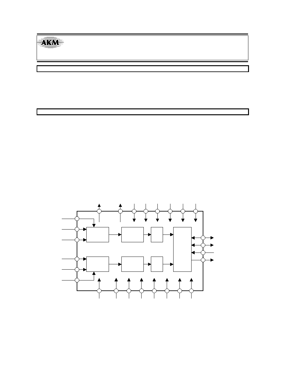
TEST
Decimation
Filter
Delta-Sigma
Modulator
Decimation
Filter
HPF
HPF
Audio I/F
Controller
DVDD
AVDD
DVSS
AVSS
VREFR
VREFL
LIN+
LIN-
Delta-Sigma
Modulator
RIN+
RIN-
DIF
PDN
LRCK
BICK
MCLK
SDTO
HPFE
M/S DFS1 DFS0 CKS1 CKS0
VCOM
BVSS
OVF
Block diagram
24Bit 192kHz
ADC
AK5385B
ASAHI KASEI
[AK5385B]
MS0406-E-00
2005/08
- 2 -
Ordering Guide
AK5385BVS
10
~
+70
°C
28pin
SOP
(1.27mm
pitch)
AK5385BVF
40
~
+85
°C
28pin
VSOP
(0.65mm
pitch)
AKD5385B Evaluation
Board
for
AK5385B
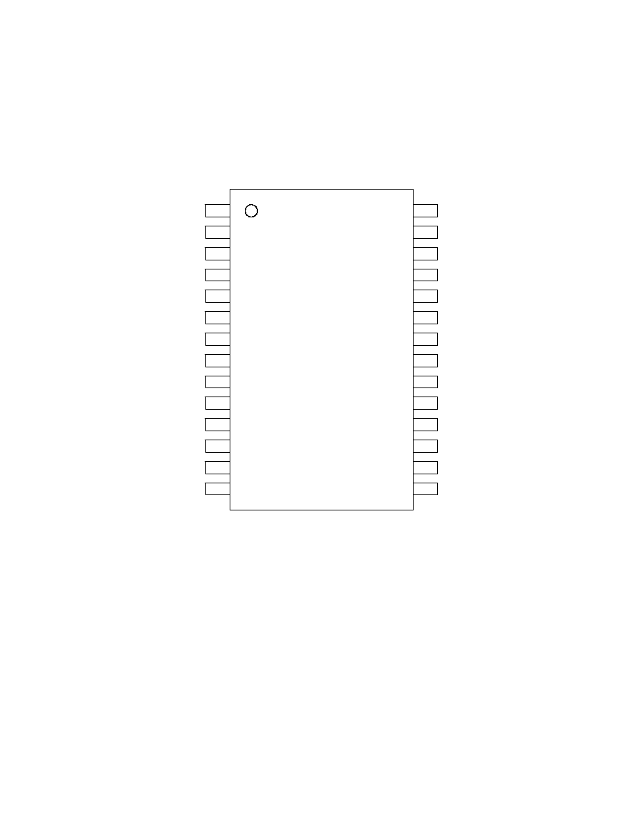
Pin Layout
VCOM
LIN+
DVDD
DVSS
VREFL
AVSS
LIN-
CKS0
PDN
DIF
M/S
LRCK
BICK
OVF
Top View
8
7
6
5
4
3
2
1
21
22
23
24
25
26
27
28
TEST
RIN+
AVSS
AVDD
RIN-
AVSS
VREFR
9
10
11
12
13
14
18
19
20
HPFE
15
16
17
SDTO
CKS1
MCLK
DFS1
BVSS
DFS0
ASAHI KASEI
[AK5385B]
MS0406-E-00
2005/08
- 3 -
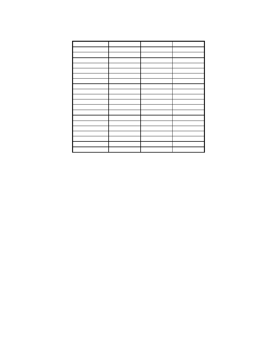
Compatibility with AK5383/AK5394A
AK5385B
AK5383
AK5394A
Pin 1
VREFL
VREFL
VREFL+
Pin 2
AVSS
GNDL
VREFL
-
Pin 3
VCOM
VCOML
VCOML
Pin 6
CKS0
ZCAL
ZCAL
Pin 9
OVF
CAL
CAL
Pin 11
DIF
SMODE2
SMODE2
Pin 12
M/S
SMODE1
SMODE1
Pin 16
CKS1
FSYNC
FSYNC
Pin 18
DFS0
DFS
DFS0
Pin
20
DFS1 TEST DFS1
Pin 26
TEST
VCOMR
VCOMR
Pin 27
AVSS
GNDR
VREFR
-
Pin 28
VREFR
VREFR
VREFR+
fs
8kHz
216kHz 1kHz 108kHz 1kHz 216kHz
MCLK at 48kHz
256/384/512fs
256fs
256fs
MCLK
at
96kHz
256fs 128fs 128fs
MCLK at 192kHz
128fs
Not Available
64fs
DR,
S/N
114dB 110dB 123dB
Input Voltage
±2.9Vpp
±2.45Vpp
±2.4Vpp
Offset Calibration
Not Available
Available
Available
ASAHI KASEI
[AK5385B]
MS0406-E-00
2005/08
- 4 -
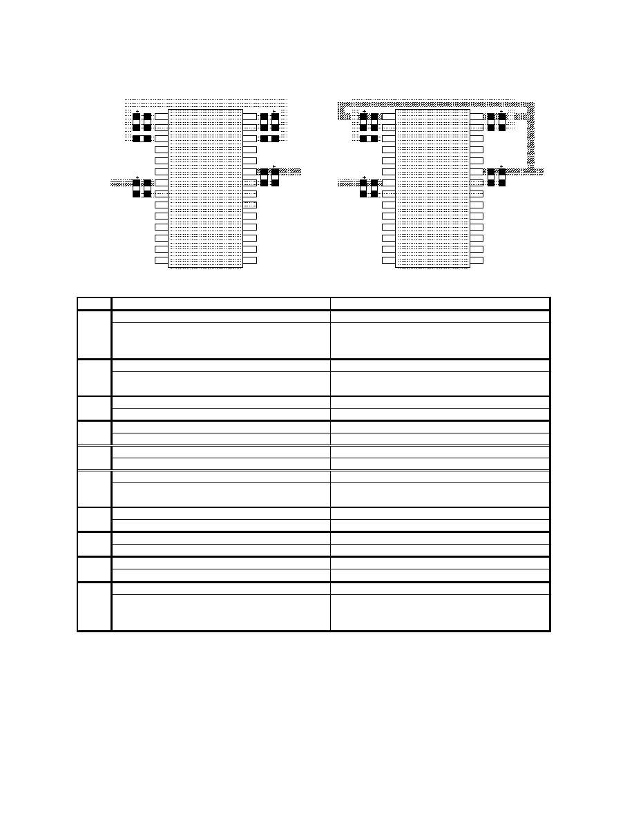
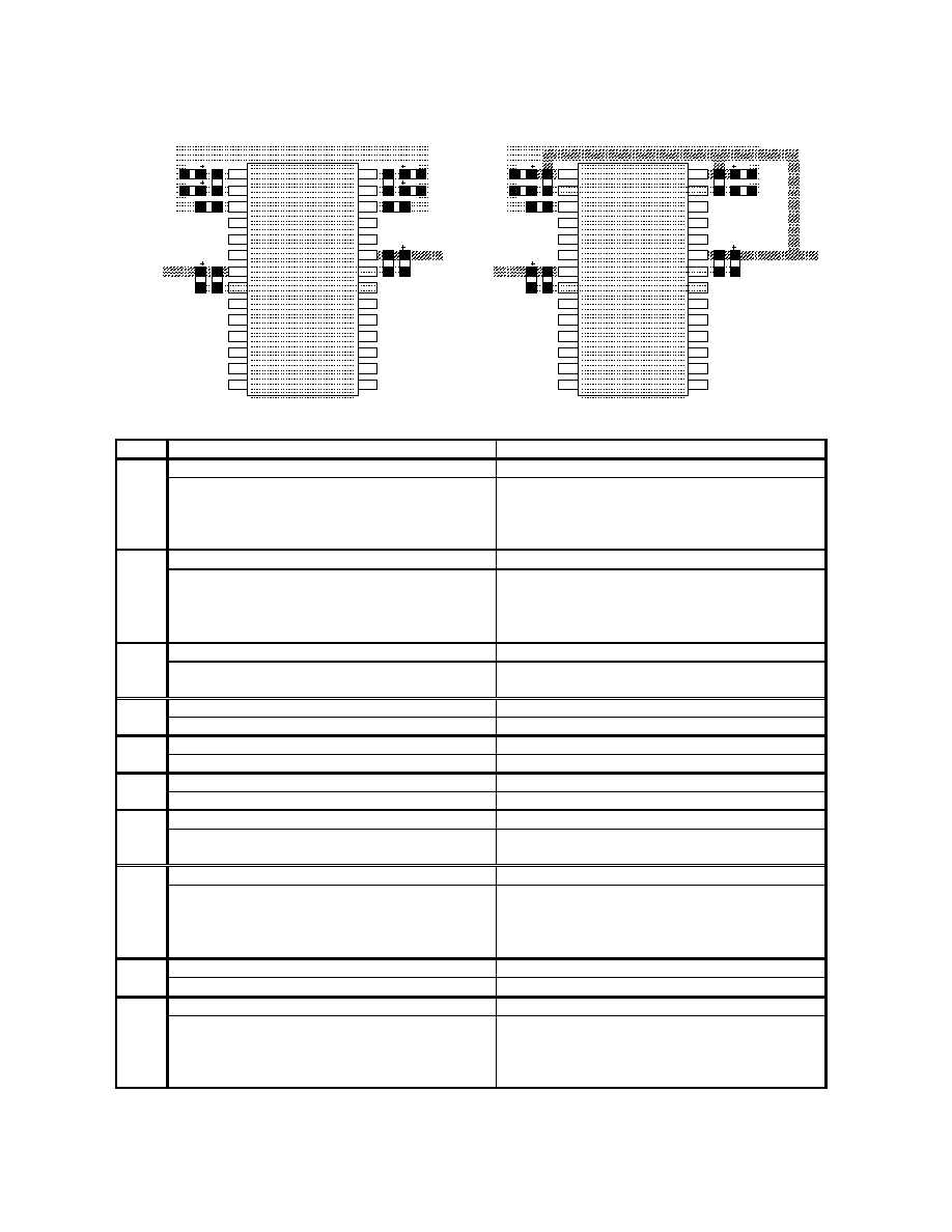
Compare PCB layout example between AK5385B and AK5383
3.0 ~ 5.25V
Digital
VREFL
GNDL
1
2
3
4
5
6
7
8
9
10
11
12
13
14
VCOML
AINL+
AINL-
ZCAL
VD
DGND
CAL
RSTN
SMODE2
SMODE1
LRCK
SCLK
28
27
26
25
24
23
22
21
20
19
18
17
16
15
VREFR
GNDR
VCOMR
AINR+
AINR-
VA
AGND
BGND
TEST
HPFE
DFS
MCLK
FSYNC
SDATA
0.1
µ
10
µ
0.22
µ
0.1
µ
10
µ
0.1
µ
10
µ
5V
Analog
Analog Ground
0.1
µ
10
µ
0.22
µ
3.0 ~ 5.25V
Digital
VREFL
AVSS
1
2
3
4
5
6
7
8
9
10
11
12
13
14
VCOM
LIN+
LIN-
CKS0
DVDD
DVSS
OVF
PDN
DIF
M/S
LRCK
BICK
28
27
26
25
24
23
22
21
20
19
18
17
16
15
VREFR
AVSS
TEST
RIN+
RIN-
AVDD
AVSS
BVSS
DFS1
HPFE
DFS0
MCLK
CKS1
SDTO
10
µ
0.22
µ
0.1
µ
10
µ
0.1
µ
10
µ
5V
Analog
10
µ
AK5385B
AK5383
0.1
µ
Analog Ground
0.1
µ
Pin #
AK5383
AK5385B
VREFL VREFL
1
Lch Voltage Reference Output Pin, 3.75V
Normally, connected to GNDL with a 10
µF
electrolytic capacitor and a 0.1
µF ceramic capacitor.
Lch Voltage Reference Input Pin, AVDD
Normally, connected to AVSS with a 10
µF
electrolytic capacitor and a 0.1
µF ceramic capacitor.
ZCAL CKS0
6
Zero Calibration Control Pin
This pin controls the calibration reference signal.
Master Clock Select 0 Pin
(Internal Pull-down Pin, typ. 100k
)
CAL OVF
9
Calibration Active Signal Pin
Analog Input Overflow Detect Pin
SMODE2 DIF
11
Serial Interface Mode Select Pin
Audio Interface Format Pin
SMODE1 M/S
12
Serial Interface Mode Select Pin
Master / Slave Mode Pin
FSYNC CKS1
16
Frame Synchronization Signal Pin
Master Clock Select 1 Pin
(Internal Pull-down Pin, typ.100k
)
DFS DFS0
18
Double Speed Sampling Mode Pin
Sampling Speed Select 0 Pin
TEST DFS1
20
Test Pin (Internal Pull-down Pin)
Sampling Speed Select 1 Pin
VCOMR TEST
26
Rch Common Voltage Pin, 2.75V
Test Pin (Internal Pull-down Pin, typ. 100k
)
VREFR VREFR
28
Rch Voltage Reference Output Pin, 3.75V
Normally, connected to GNDL with a 10
µF
electrolytic capacitor and a 0.1
µF ceramic capacitor.
Rch Voltage Reference Input Pin, AVDD
Normally, connected to AVSS with a 10
µF
electrolytic capacitor and a 0.1
µF ceramic capacitor.
ASAHI KASEI
[AK5385B]
MS0406-E-00
2005/08
- 5 -
Compare PCB layout example between AK5385B and AK5394A
3.0 ~ 5.25V
Digital
VREFL+
VREFL-
1
2
3
4
5
6
7
8
9
10
11
12
13
14
VCOML
AINL+
AINL-
ZCAL
VD
DGND
CAL
RSTN
SMODE2
SMODE1
LRCK
SCLK
28
27
26
25
24
23
22
21
20
19
18
17
16
15
VREFR+
VREFR-
VCOMR
AINR+
AINR-
VA
AGND
BGND
DFS1
HPFE
DFS0
MCLK
FSYNC
SDATA
0.1
µ
10
µ
0.22
µ
0.1
µ
10
µ
0.1
µ
10
µ
5V
Analog
Analog Ground
0.1
µ
10
µ
0.22
µ
AK5394A
10
µ
10
µ
3.0 ~ 5.25V
Digital
VREFL
AVSS
1
2
3
4
5
6
7
8
9
10
11
12
13
14
VCOM
LIN+
LIN-
CKS0
DVDD
DVSS
OVF
PDN
DIF
M/S
LRCK
BICK
28
27
26
25
24
23
22
21
20
19
18
17
16
15
VREFR
AVSS
TEST
RIN+
RIN-
AVDD
AVSS
BVSS
DFS1
HPFE
DFS0
MCLK
CKS1
SDTO
0.1
µ
10
µ
0.22
µ
0.1
µ
10
µ
0.1
µ
10
µ
5V
Analog
0.1
µ
10
µ
AK5385B
(short)
(short)
Analog Ground
Pin #
AK5394A
AK5385B
VREFL+ VREFL
1
Lch Positive Voltage Reference Output Pin, 3.75V
Normally connected to AGND with a large
electrolytic capacitor and connected to VREFL
-
with a 0.22
µF ceramic capacitor.
Lch Voltage Reference Input Pin, AVDD
Normally, connected to AVSS with a 10
µF
electrolytic capacitor and a 0.1
µF ceramic capacitor.
VREFL
-
AVSS
2
Lch Negative Voltage Reference Output Pin, 1.25V
Normally connected to AGND with a large
electrolytic capacitor and connected to VREFL+
with a 0.22
µF ceramic capacitor.
Analog Ground Pin
ZCAL CKS0
6
Zero Calibration Control Pin
This pin controls the calibration reference signal.
Master Clock Select 0 Pin
(Internal Pull-down Pin, typ. 100k
)
CAL OVF
9
Calibration Active Signal Pin
Analog Input Overflow Detect Pin
SMODE2 DIF
11
Serial Interface Mode Select Pin
Audio Interface Format Pin
SMODE1 M/S
12
Serial Interface Mode Select Pin
Master / Slave Mode Pin
FSYNC CKS1
16
Frame Synchronization Signal Pin
Master Clock Select 1 Pin
(Internal Pull-down Pin, typ. 100k
)
VREFR
-
AVSS
27
Rch Negative Voltage Reference Output Pin, 1.25V
Normally connected to AGND with a large
electrolytic capacitor and connected to VREFR+
with a 0.22
µF ceramic capacitor.
Analog Ground Pin
VCOMR TEST
26
Rch Common Voltage Pin, 2.75V
Test Pin (Internal Pull-down Pin, typ. 100k
)
VREFR+ VREFR
28
Rch Positive Reference Output Voltage, 3.75V
Normally connected to AGND with a large
electrolytic capacitor and connected to VREFR
-
with a 0.22
µF ceramic capacitor.
Rch Voltage Reference Input Pin, AVDD
Normally, connected to AVSS with a 10
µF
electrolytic capacitor and a 0.1
µF ceramic capacitor.