 | –≠–ї–µ–Ї—В—А–Њ–љ–љ—Л–є –Ї–Њ–Љ–њ–Њ–љ–µ–љ—В: AK6480AM | –°–Ї–∞—З–∞—В—М:  PDF PDF  ZIP ZIP |
ASAHI KASEI
[AK6420A/40A/80A]
DAS01E-00
1999/05
- 1 -
AK6420A / 40A / 80A
2K / 4K / 8Kbit Serial CMOS EEPROM
Features
ADVANCED CMOS EEPROM TECHNOLOGY
Wide Vcc (1.8V
5.5V) operation
AK6420A
Ј
Ј
2048 bits: 128
„
16 organization
AK6440A
Ј
Ј
4096 bits: 256
„
16 organization
AK6480A
Ј
Ј
8192 bits: 512
„
16 organization
ONE CHIP MICROCOMPUTER INTERFACE
- Interface with one chip microcomputer's serial communication port directly
LOW POWER CONSUMPTION
- 0.75mA Max (Read operation)
- 0.8
µ
A Max (Standby mode)
HIGH RELIABILITY
-Endurance
: 100K cycles
-Data Retention
: 10 years
SPECIAL FEATURES
- High speed operation ( f
MAX
=1MHz: Vcc=2.5V )
- Automatic write cycle time-out with auto-ERASE
- Automatic address increment (READ)
- Ready/Busy status signal
- Software and Hardware controlled write protection
IDEAL FOR LOW DENSITY DATA STORAGE
- Low cost, space saving, 8-pin package (SOP, SSOP)
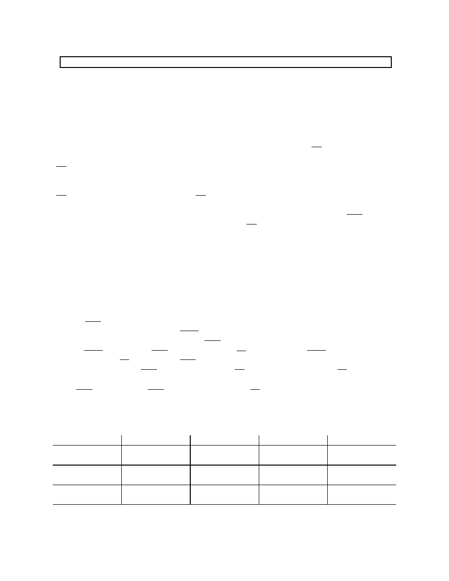
Block diagram
ASAHI KASEI
[AK6420A/40A/80A]
DAS01E-00
1999/05
- 2 -
General Description
The AK6420A/40A/80A is a 2048/4096/8192bit, serial, read/write, non-volatile memory device fabricated using an
advanced CMOS EEPROM technology. The AK6420A has 2048bits of memory organized into 128 registers of 16
bits each. The AK6440A has 4096bits of memory organized into 256 registers of 16 bits each. The AK6480A has
8192bits of memory organized into 512 registers of 16 bits each. The AK6420A/40A/80A can operate full function
under wide operating voltage range from 1.8V to 5.5V. The charge up circuit is integrated for high voltage generation
that is used for write operation.
The AK6420A/40A/80A can connect to the serial communication port of popular one chip microcomputer directly (3
line negative clock synchronous interface). At write operation, AK6420A/40A/80A takes in the write data from data
input pin (DI) to a register synchronously with rising edge of input pulse of serial clock pin (SK). And at read operation,
AK6420A/40A/80A takes out the read data from a register to data output pin (DO) synchronously with falling edge of
SK.
The AK6420A/40A/80A has 4 instructions such as READ, WRITE, WREN (write enable) and WRDS (write disable).
Each instruction is organized by op-code block (8bits), address block (8bits) and data (8bits
„
2). When input level of
SK pin is high level and input level of chip select (CS) pin is changed from high level to low level, AK6420A/40A/80A
can receive the instructions.
Special features of the AK6420A/40A/80A include : automatic write time-out with auto-ERASE, Ready/Busy status
signal output and ultra-low standby power mode when deselected (CS=high).
Ј
Software and Hardware controlled write protection
The AK6420A/40A/80A has 2 (hardware and software) write protection functions.
After power on or after execution of WRDS (write disable) instruction, execution of WRITE instruction will be disabled.
This write protection condition continues until WREN instruction is executed or Vcc is removed from the part.
Execution of READ instruction is independent of both WREN and WRDS instructions.
Reset pin should be low level when WRITE instruction is executed. When the Reset pin is high level, the WRITE
instruction is not executed.
Ј
Ready/Busy status signal
During the automatic write time-out period (BUSY status), the AK6420A/40A/80A can't accept the other instructions.
The AK6420A/40A/80A has 2 functions to know the Busy status from exterior.
The RDY/BUSY pin indicates the Busy status regardless of the CS pin status. The RDY/BUSY pin outputs the low
level regardless of the CS pin status during Busy status. Except the above status, this pin outputs high level.
Also the DO pin indicates the Busy status. When input level of SK pin is low level and input level of CS pin is changed
from high level to low level, the AK6420A/40A/80A is in the status output mode and the DO pin indicates the
Ready/Busy status. The Ready/Busy status outputs on DO pin until CS pin is changed from low level to high level, or
first bit ("1") of op-code of next instruction is given to the part. Except when the device is in the status output mode or
outputs data, the DO pin is in the high impedance state.
Type of Products
Model
Memory size
Temp.Range
Vcc
Package
AK6420AF
AK6420AM
2Kbits
-40
∞
C
85
∞
C
-40
∞
C
85
∞
C
1.8V
5.5V
1.8V
5.5V
8pin Plastic SOP
8pin Plastic SSOP
AK6440AF
AK6440AM
4Kbits
-40
∞
C
85
∞
C
-40
∞
C
85
∞
C
1.8V
5.5V
1.8V
5.5V
8pin Plastic SOP
8pin Plastic SSOP
AK6480AF
AK6480AM
8Kbits
-40
∞
C
85
∞
C
-40
∞
C
85
∞
C
1.8V
5.5V
1.8V
5.5V
8pin Plastic SOP
8pin Plastic SSOP
ASAHI KASEI
[AK6420A/40A/80A]
DAS01E-00
1999/05
- 3 -
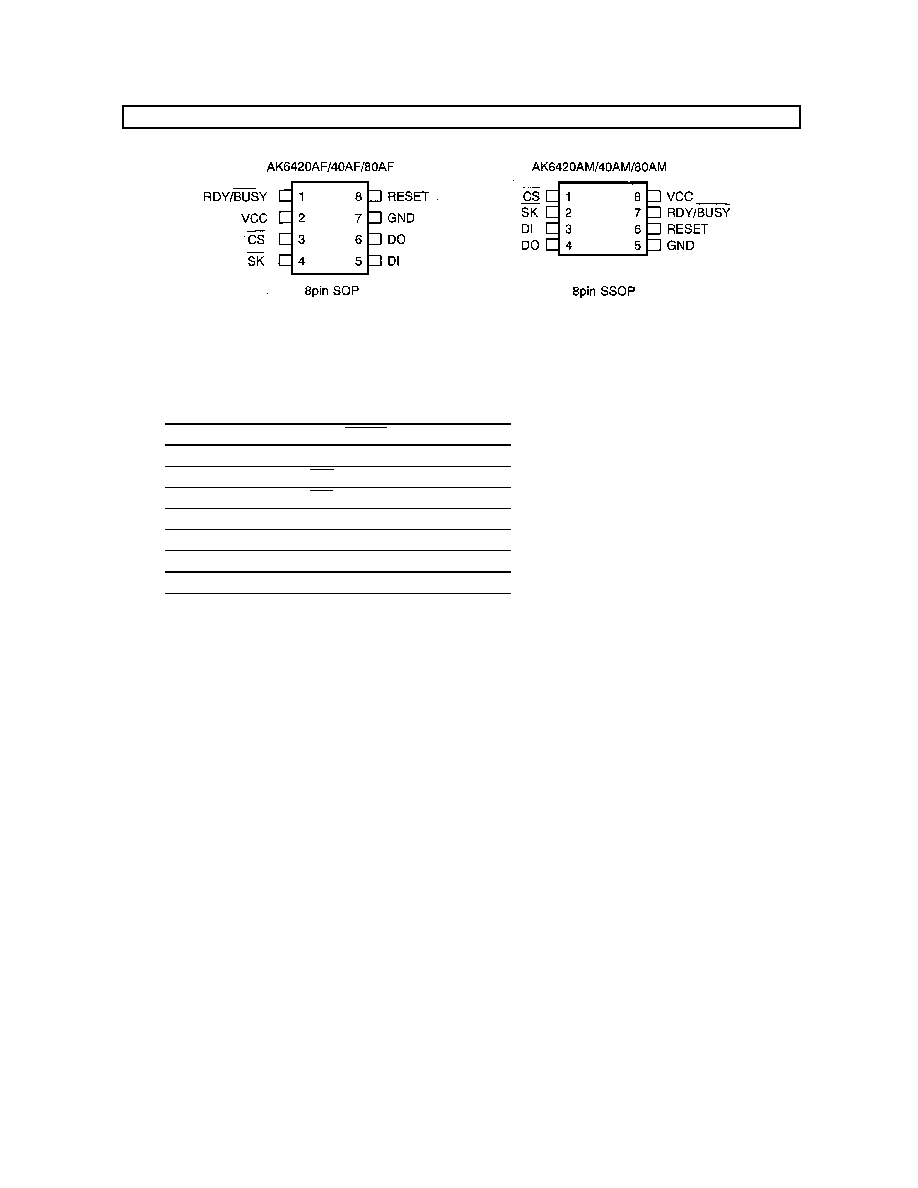
Pin arrangement
Pin Function
Pin No.
Pin name
I/O
SOP / SSOP
1 / 7
RDY/BUSY
O
2 / 8
Vcc
3 / 1
CS
I
4 / 2
SK
I
5 / 3
DI
I
6 / 4
DO
O
7 / 5
GND
8 / 6
RESET
I
Note
I : Input pin
O: Output pin

ASAHI KASEI
[AK6420A/40A/80A]
DAS01E-00
1999/05
- 4 -
Pin Description
CS (Chip Select)
When SK is high level and CS is changed from high level to low level, AK6420A/40A/80A can receive the
instructions. CS should be kept low level while receiving op-code, address and data and while outputting data.
If CS is changed to high level during the above period, AK6420A/40A/80A stops the instruction execution.
When SK is low and CS is changed from high level to low level, AK6420A/40A/80A will be in status output
mode. The CS need not be low level during the automatic write time-out period (BUSY status).
SK (Serial Clock)
The SK clock pin is the synchronous clock input for input/output data. At write operation, AK6420A/40A/80A
takes in the write data from data input pin (DI) synchronously with rising edge of input pulse of serial clock pin
(SK). And at read operation, AK6420A/40A/80A takes out the read data to data output pin (DO)
synchronously with falling edge of SK. The SK clock is not needed during the automatic write time-out period
(BUSY status), the status output period and when the device isn't selected (CS = high level).
DI (Data Input)
The op-code, address and write data is input to the DI pin.
DO (Data Output)
The DO pin outputs the read data and status signal and will be high impedance except for this timing.
RDY/BUSY (Ready/Busy status)
This pin outputs the internal programming status. When the AK6420A/40A/80A is in the automatic write time-
out period, this pin outputs the low level (BUSY status), and outputs the high level except for this timing.
RESET (Reset)
The AK6420A/40A/80A stops executing the write instruction when the RESET pin is high level. The RESET
pin should be low level while the write instruction input period and the automatic write time-out period. If the
RESET pin is high level while the automatic write time-out period, the AK6420A/40A/80A stops execution of
internal programming and the device returns to ready status. In this case the word data of the specified
address will be incomplete. When inputting the new instruction after RESET, the CS should be set to high
level. The read, write enable and write disable instructions are not affected by RESET pin status.
Vcc (Power Supply)
GND (Ground)
ASAHI KASEI
[AK6420A/40A/80A]
DAS01E-00
1999/05
- 5 -
Functional Description
The AK6420A/40A/80A has 4 instructions such as READ, WRITE, WREN (write enable) and WRDS (write
disable). Each instruction is organized by op-code block (8bits), address block (8bits) and data (8bits
„
2).
When input level of SK pin is high level and input level of chip select (CS) pin is changed from high level to low
level, AK6420A/40A/80A can receive the instructions.
When the instructions are executed consecutively, the CS pin should be brought to high level for a minimum of
250ns(Tcs) between consecutive instruction cycle.
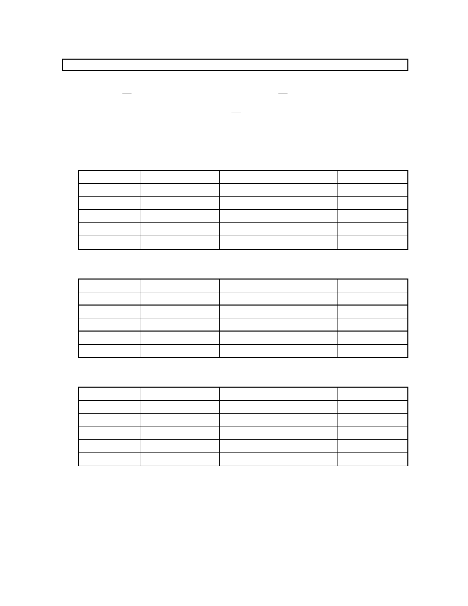
Instruction Set For 6420A
Instruction
Op-Code
Address
Data
READ
1 0 1 0 1 0 0 0
A6 A5 A4 A3 A2 A1 A0 0
D15 -D0
WRITE
1 0 1 0 0 1 0 0
A6 A5 A4 A3 A2 A1 A0 0
D15 -D0
WREN
1 0 1 0 0 0 1 1
эээ’ээ’ээ’ээ’ээ’ээ’ээ’ээ’
WRDS
1 0 1 0 0 0 0 0
эээ’ээ’ээ’ээ’ээ’ээ’ээ’ээ’
( WRAL )
1 0 1 0 1 1 1 1
э э э ’ээ’ээ’ээ’ээ’ээ’ээ’ээ’
D15 -D0
Instruction Set For 6440A
Instruction
Op-Code
Address
Data
READ
1 0 1 0 1 0 0 0
A7 A6 A5 A4 A3 A2 A1 A0
D15 -D0
WRITE
1 0 1 0 0 1 0 0
A7 A6 A5 A4 A3 A2 A1 A0
D15 -D0
WREN
1 0 1 0 0 0 1 1
э э э ’ээ’ээ’ээ’ээ’ээ’ээ’ээ’
WRDS
1 0 1 0 0 0 0 0
э э э ’ээ’ээ’ээ’ээ’ээ’ээ’ээ’
( WRAL )
1 0 1 0 1 1 1 1
э э э ’ээ’ээ’ээ’ээ’ээ’ээ’ээ’
D15 -D0
Instruction Set For 6480A
Instruction
Op-Code
Address
Data
READ
1 0 1 0 1 0 0 A8
A7 A6 A5 A4 A3 A2 A1 A0
D15 -D0
WRITE
1 0 1 0 0 1 0 A8
A7 A6 A5 A4 A3 A2 A1 A0
D15 -D0
WREN
1 0 1 0 0 0 1 1
э э э ’ээ’ээ’ээ’ээ’ээ’ээ’ээ’
WRDS
1 0 1 0 0 0 0 0
э э э ’ээ’ээ’ээ’ээ’ээ’ээ’ээ’
( WRAL )
1 0 1 0 1 1 1 1
э э э ’ээ’ээ’ээ’ээ’ээ’ээ’ээ’
D15 -D0
’
:don't care
(Note) The WRAL instruction is used for factory function test only. User can't use this instruction .