
[ASAHI KASEI]
[AK7746]
[MS0369-E00]
- 1 -
2004/12
The AK7746 is a highly integrated audio processor, including 5 A/D channels, an input mux that can select 2 stereo pairs
from 8 stereo inputs, and an on-chip DSP. High quality analog performance is provided by the ADC's achieving 98dB
(48kHz) dynamic range. The A/D supports sampling frequencies from 8kHz to 96kHz. The AK7746 includes 72kbits of
SRAM for audio delay that is suitable for simulated surround functions and speaker compensation. The programmable
DSP allows up to 4608 execution lines per audio sample cycle at 8kHz, 768 lines at 48kHz, or 384 lines at 96kHz with
multiple functions per line. The AK7746 can be used to implement complete sound field control, such as echo, 3D,
parametric equalization, etc. It is packaged in a 64-lead LQFP.
1.
General
Description
2. Features
DSP:
-
Word length:
24-bit (Data RAM)
-
Instruction cycle time:
27ns (768fs, fs=48kHz )
-
Multiplier:
24 x 16
40-bit
-
Divider:
24 / 24
16-bit or 24-bit
-
ALU:
34-bit arithmetic operation (Overflow margin: 4bit)
-
24-bit arithmetic and logic operation
-
Shift+Register:
1, 2, 3, 4, 6, 8 and 15 bits shifted left
1, 2, 3, 4, 8 and 15 bits shifted right
(Other numbers in parentheses are restricted.
Provided with indirect shift function)
-
Program RAM:
768 x 32-bit
-
Coefficient RAM:
1024 x 16-bit
-
Data
RAM:
256
x
24-bit
-
Offset RAM:
48 x 13-bit
(6144 x 12-bit / 3072 x 24-bit / 4096 x 12-bit + 1024 x 24-bit )
-
Internal
Memory:
72kbit
SRAM
-
Sampling frequency:
8kHz to 96kHz
-
Serial interface port for micro-controller
-
Master clock:
768fs@48kHz ( generated by PLL from 256fs or 384fs )
-
Master/Slave operation
-
Serial signal input port ( 8(10) ch ):16/20/24-bit : Output port ( 8ch + 4ch ): 24-bit
ADC:
4 channels (2 channels 2 sets )
-
24-bit 64 x Over-sampling delta sigma
-
Sampling frequency:
8kHz to 96kHz
-
DR:
98dBA ( fs=48 kHz Full-differential Input )
-
S/N :
98dBA ( fs=48 kHz Full-differential Input )
-
S/(N+D) :
91dB ( fs= 48 kHz Full-differential Input )
-
Digital HPF (fc = 1Hz)
-
Single-ended or Full-differential Input
ADC:
Monaural 1 channel
-
24-bit 64x Over-sampling delta sigma
-
Sampling frequency:
8kHz to 96kHz
-
DR:
97dBA ( fs=48 kHz )
-
S/N :
97dBA ( fs=48 kHz )
-
S/(N+D) :
91dB ( fs= 48 kHz )
Other
-
External Jump pin:
3(maximum)
-
CRC error check function
-
LRCLK and BITCLK input and output for slave mode
-
Power
supply:
+3.3V
�0.3V
-
Operating temperature range:
-40
�C~85�C
-
Package:
64pin LQFP (0.5mm pitch)
Audio DSP with 5-channel 24-bit ADC and Input Mux
AK7746
[ASAHI KASEI]
[AK7746]
[MS0369-E00]
- 5 -
2004/12
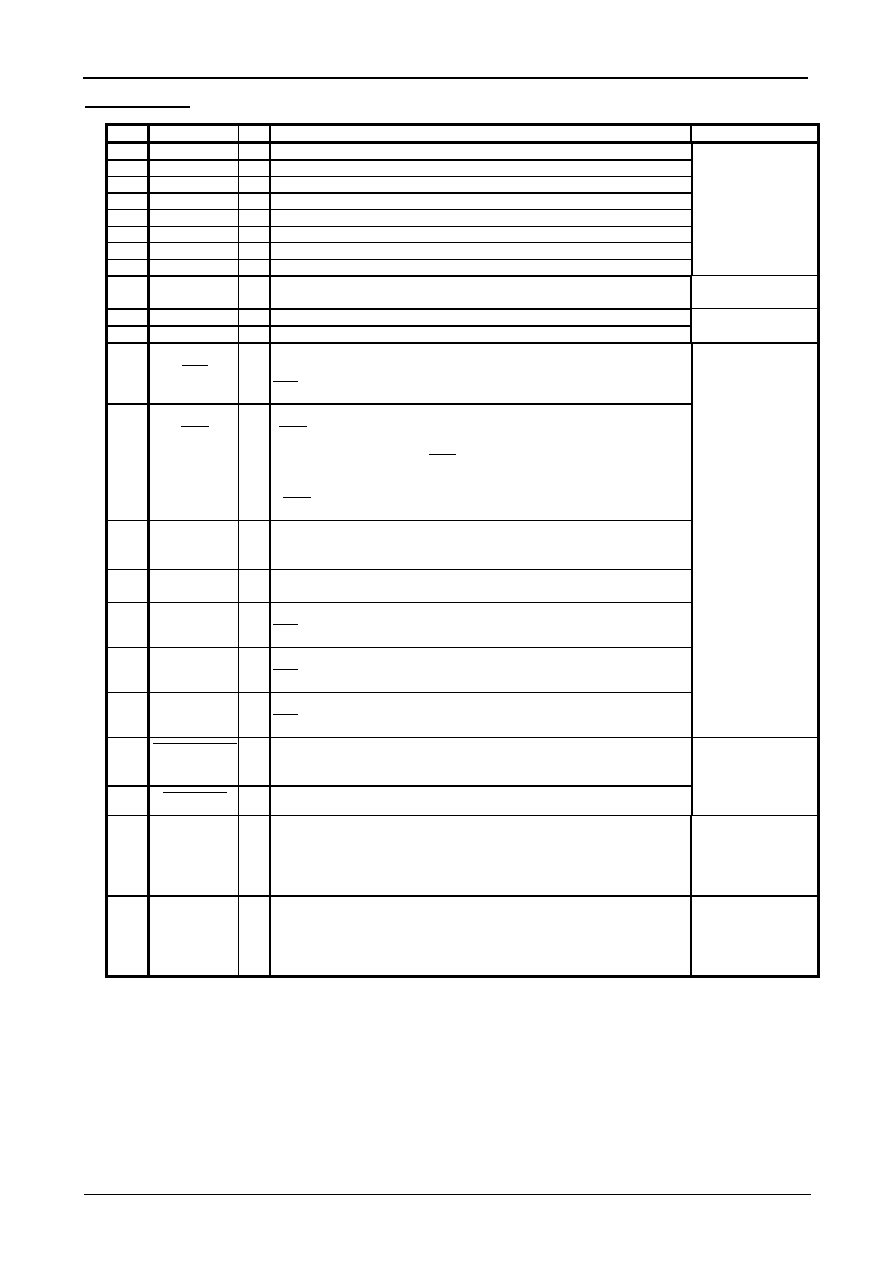
(2) Pin function
Pin No
Pin name
I/O
Function Classification
1 AINR5 I
ADC1 or ADC2 Rch single ended analog input 5
2 AINL5 I
ADC1 or ADC2 Lch single ended analog input 5
3 AINR6 I
ADC1 or ADC2 Rch single ended analog input 6
4 AINL6 I
ADC1 or ADC2 Lch single ended analog input 6
5 AINR7 I
ADC1 or ADC2 Rch single ended analog input 7
6 AINL7 I
ADC1 or ADC2 Lch single ended analog input 7
7 AINR8 I
ADC1 or ADC2 Rch single ended analog input 8
8 AINL8 I
ADC1 or ADC2 Lch single ended analog input 8
Analog input
9 BVSS -
Analog ground (Silicon base ground level)
Connect with AVSS pin
Analog Power supply
10 DVSS -
Digital Ground 0.0V
11 DVDD -
Digital power supply 3.3V(typ)
Digital Power supply
12
CS
I
Chip select pin for Microcomputer interface. (Internal pull-down)
Normaly leave OPEN or connect with DVSS.
CS ="H" : SI can not input, SO,RDY,DRDY = Hi-Z.
13
RQ
I
Write request pin for Microcomputer interface.
RQ ="L" : Microcomputer interface enable.
For run-time data read out: RQ ="H".
When Microcomputer interface is not used or during initial reset, leave
RQ ="H".
14
SI
I
Serial data input and serial data output control pin for Microcomputer
interface.
When SI is not used, leave SI="L".
15 SCLK I
Serial data clock pin for Microcomputer interface.
When SCLK is not used, leave SCLK="H".
16 SO O
Serial data output pin for Microcomputer interface.
CS ="H" : SO = Hi-Z.
17 RDY O
Data write ready output pin for Microcomputer interface.
CS ="H" : RDY = Hi-Z.
18 DRDY O
Output data ready pin for Microcomputer interface.
CS ="H" : DRDY = Hi-Z.
Microcomputer
Interface
19
INIT_RESET
I Reset pin ( for initialization )
Used for initialization of the AK7746. When changing CKS1 or CKS0 and
changing XTI input frequency, this pin setting is necessary.
20
S_RESET
I System Reset pin
Reset
21 SDIN4/JX2 I
DSP serial data input pin / External condition jump pin
(Internal pull-down )
* Compatible with MSB justified 24 bits / LSB justified 24,20 and 16 bits
* It can change its function as a conditional jump pin JX2 by control register
setting (JX2_E).
Digital section
Serial input data /
Conditional input
22 SDIN3/JX1 I
DSP serial data input pin / External condition jump pin
(Internal pull-down )
* Compatible with MSB justified 24 bits / LSB justified 24,20 and 16 bits
* It can change its function as a conditional jump pin JX1 by control register
setting (JX1_E).
Digital section
Serial input data /
Conditional input


