ASAHI KASEI
[AKD4117-B]
<KM077200>
2004/12
-
1
-
GENERAL DESCRIPTION
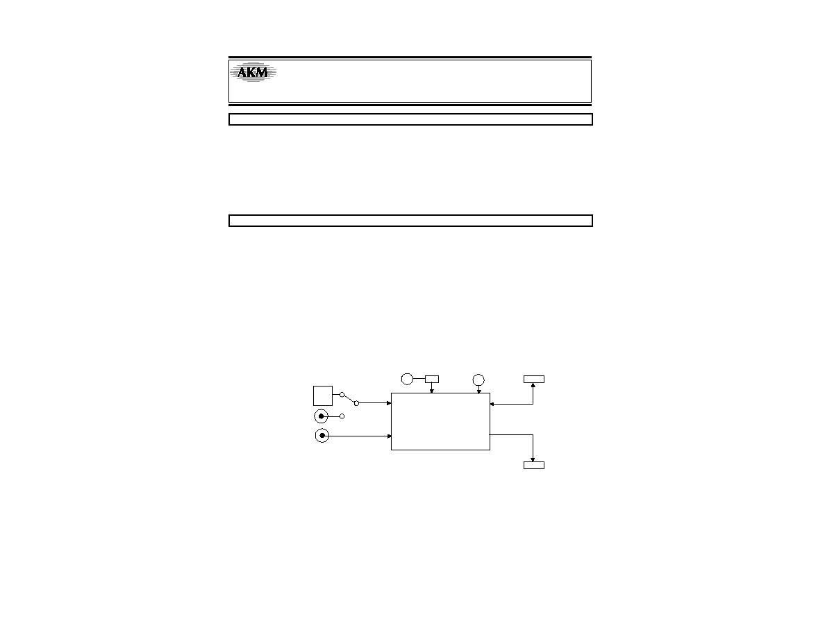
AKD4117-B is the evaluation board for AK4117, 192kHz digital audio receiver. This board has optical
connector and BNC connector to interface with other digital audio equipment.
Ordering guide
AKD4117-B --- Evaluation board for AK4117
(A cable for connecting with printer port of IBM-AT compatible PC
and a control software are packed with this. The control software
does not operate on Windows NT.)
FUNCTION
Digital interface
-S/PDIF :
8 channel input (optical or BNC)
- Serial audio data I/F :
1 output (for DIR data output. 10-pin port)
-U bit :
-Serial control data I/F
1 input/output port (10-pin port)
RX0
RX1
AK4117
Control
5V GND
Opt
Serial Data out
(From DIR)
REG
3.3V
Figure 1. AKD4117-B Block Diagram
*Circuit diagram and PCB layout are attached at the end of this manual.
AK4117 Evaluation Board Rev.0
AKD4117-B

ASAHI KASEI
[AKD4117-B]
<KM077200>
2004/12
-
2
-
Evaluation Board Manual
Operating sequence
(1) Set up the power supply lines.
[+ 5V] (Red) = 5V
[GND] (Black) = 0V
(2)
Set up the evaluation mode and jumper pins. (Refer to the following item.)
(3)
Connect cables. (Refer to the following item.)
(4)
Power on.
The AK4117 should be reset once bringing PDN(SW2) "L" upon power-up.
Evaluation modes
(1) Evaluation for DIR
S/PDIF
Optical or BNC
connector
PORT2
(10pin Header)
MCLK
BICK
LRCK
SDTO
AK4117
(DIR)
AKD4117-B
DAC
MCLK
BICK
LRCK
SDTO
The DIR generates MCLK, BICK, LRCK and SDATA from the received data through optical
connector(PORT1: TORX176) or BNC connector . The AKD4117-B can be connected with the AKM's DAC
evaluation board via 10-line cable.
a. Set-up of Bi-phase Input
RX0 and RX1 should not select BNC at the same time.
a-1. RX0
Connector JP2(RX0)
Optical (PORT1)
OPT
BNC (J2)
BNC
Table 1. Set-up of RX0
When S/PDIF signal is inputted from PORT1 (optical), JP19 should be short.
a-2. RX1 can be inputted from a BNC (J2) connector only.
Input RX1
JP4
JP
Short
Table 2. Set-up of RX1

ASAHI KASEI
[AKD4117-B]
<KM077200>
2004/12
-
3
-
a-3. Set-up of AK4117 input path
IPS bit
Input data
0 RX0
Default
1 RX1
Table 3. Recovery Data Select
b. Set-up of clock input and output
The signal level outputted/inputted from PORT2 is 3.3V.
PORT2
DIR
5
6
1
10
GND
GND
GND
GND
N
C
MCL
K
BI
C
K
LR
CK
SDTO
DAU
X
Figure 2. PORT2 pin layout
b-1. MCKO1/MCKO2
The AK4117 has a master clock output pin, MCKO. In PLL mode, PCKS1-0 bits select the MCKO frequency as
shown in
Table 4
. When MCKO=512fs, MCKO goes to "L" when fs=96kHz and 192kHz. When MCKO=256fs,
MCKO goes to "L" when fs=192kHz. When LP bit is set to "1", the AK4117 is in low power mode (default). In
low power mode, PLL lock range is up to 48kHz and the MCKO frequency is fixed to 256fs.
In the X'tal mode, XCKS1-0 bits select the ratio of the X'tal frequency to fs (sampling frequency). The DIV bit
selects the ratio (x1 or x1/2) of the MCKO frequency to the X'tal frequency (
Table 5
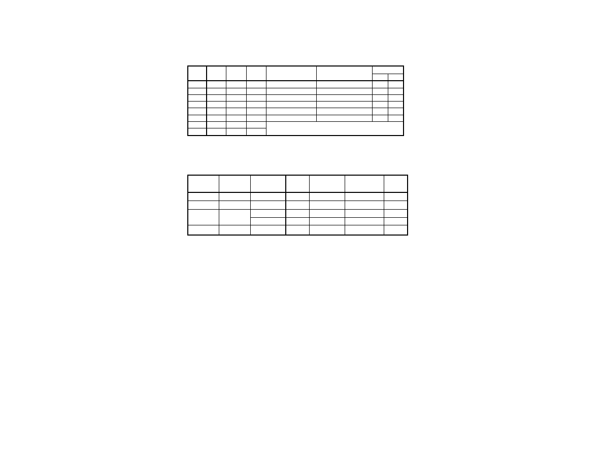
).
LP PCKS1
PCKS0
MCKO
fs
[kHz]
0 0
512fs
32
48
0 1
256fs
32 96
1 0
128fs
32 192
0
1 1
N/A
N/A
1
x x
256fs
32 48
Default
Table 4. Master Clock Frequency Select
(PLL mode: Clock operation mode 0, 2(UNLCK=0))
fs [kHz]
MCKO
EXTCLK [MHz]
X'tal [MHz]
XCKS1 XCKS0
X'tal
or
EXT
DIV=0 DIV=1 2.048 4.096 8.192 11.2896 12.288 24.576
0 0
128fs
128fs
64fs
16 32 64
88.2
96
192
0 1
256fs
256fs
128fs
8 16 32
44.1
48 96
Default
1 0
512fs
512fs
256fs
N/A 8 16
N/A
N/A
48
1 1
1024fs
1024fs
512fs
N/A
N/A
8 N/A
N/A
N/A
Table 5. Master Clock Frequency Select
(X'tal mode: Clock operation mode 1, 2(UNLCK=1), 3)
ASAHI KASEI
[AKD4117-B]
<KM077200>
2004/12
-
4
-
c. Set-up of Audio format
Please set up DIF2-0 bit.
LRCK
Mode
DIF2
bit
DIF1
bit
DIF0
bit
DAUX SDTO
I/O
0
0
0
0
24bit, Left justified
16bit, Right justified
H/L
O
1
0
0
1
24bit, Left justified
18bit, Right justified
H/L
O
2
0
1
0
24bit, Left justified
20bit, Right justified
H/L
O
3
0
1
1
24bit, Left justified
24bit, Right justified
H/L
O
4
1
0
0
24bit, Left justified
24bit, Left justified
H/L
O
Default
5 1 0 1
24bit,
I
2
S 24bit,
I
2
S L/H
O
6 1 1 0
7 1 1 1
Reserved
Table 6. Audio format
d. Set-up of CM1 and CM0
The operation mode of PLL is selected by CM1 and CM0. It can be selected by CM1-0 bits.
CM1 bit
CM0 bit
(UNLOCK)
PLL
X'tal
Clock source
SDTO
source
0
0
-
ON
ON(Note 1)
PLL(RX)
RX
Default
0 1
-
OFF
ON X'tal
DAUX
0 ON ON PLL(RX)
RX
1 0
1 ON ON X'tal
DAUX
1 1
-
ON
ON X'tal
DAUX
ON: Oscillation (Power-up), OFF: STOP (Power-Down)
Note: When the X'tal is not used as clock comparison for fs detection (XTL0, 1= "1,1"), the X'tal is OFF.
Table 7. Clock Operation Mode Select

ASAHI KASEI
[AKD4117-B]
<KM077200>
2004/12
-
5
-
U output
U(user data) can be monitored by TP1: U.
Serial control
The AK4117 can be controlled via the printer port (parallel port) of IBM-AT compatible PC. Connect PORT6
(uP-I/F) with PC by 10-line flat cable packed with the AKD4117-B. Take care of the direction of connector. There
is a mark at pin#1. The pin layout of PORT6 is as
Figure 3
.
PORT6
uP I/F
10
9
2
1
NC
CD
T
O
CD
TI
CC
L
K
CS
N
GN
D
GN
D
GN
D
GN
D
GN
D
Figure 3. PORT6 pin layout
This evaluation board encloses control software. A software operation procedure is included in an evaluation board
manual.

ASAHI KASEI
[AKD4117-B]
<KM077200>
2004/12
-
6
-
Toggle switch set-up
SW2
PDN
Reset switch for AK4117. Set to "H" during normal operation. Bring to "L" once after the
power is supplied.
LED indication
LE1
INT0
Bright when INT0 pin goes to "H".
LE2
INT1
Bright when INT1 pin goes to "H".
Set-up of XTL1 and XTL0
SW3_6 SW3_5
X'tal
Frequency
XTL1
XTL0
X'tal #1
0 0
11.2896MHz Default
0 1
12.288MHz
1 0
24.576MHz
1
1
(Use channel status)
Table 8. Reference X'tal frequency
Jumper set up.
No.
Jumper Name Function
2 RX0
Set-up of RX0 input circuit.
OPT : Optical (default)
BNC : BNC
4
RX1
Set-up of RX1 input circuit.

ASAHI KASEI
[AKD4117-B]
<KM077200>
2004/12
-
7
-
Control Software Manual
Set-up of evaluation board and control software
1. Set up the AKD4117-B according to previous term.
2. Connect IBM-AT compatible PC with AKD4117-B by 10-line type flat cable (packed with AKD4117-B). Take care
of the direction of 10pin header. (Please install the driver in the CD-ROM when this control software is used on
Windows 2000/XP. Please refer "Installation Manual of Control Software Driver by AKM device control software".
In case of Windows95/98/ME, this installation is not needed. This control software does not operate on Windows
NT.)
3. Insert the CD-ROM labeled "AKD4117-B Evaluation Kit" into the CD-ROM drive.
4. Access the CD-ROM drive and double-click the icon of "akd4117-b0.exe" to set up the control program.
5. Then please evaluate according to the follows.
Operation flow
Keep the following flow.
1. Set up the control program according to explanation above.
2. Click "Write default" button.
3. Then set up the dialog and input data.
Explanation of each buttons
1. [Port Setup] : Set up the printer port.
2. [Write default] : Initialize the register of AK4117.
3. [All Write] : Write all registers that is currently displayed.
4. [Read All] : All the registers of AK4117 are read.
5. [Function1] : Dialog to write data by keyboard operation.
6.
[F3]
:
Dialog
of
sequential
writing.
7. [SAVE] : Save the current register setting.
8. [OPEN] : Write the saved values to all register.
9. [Write] : Dialog to write data by mouse operation.
10. [Read] : The data corresponding to each register is read.

ASAHI KASEI
[AKD4117-B]
<KM077200>
2004/12
-
8
-
Explanation of each dialog
1. [Function1 Dialog] : Dialog to write data by keyboard operation
Address Box: Input register address in 2 figures of hexadecimal.
Data Box: Input register data in 2 figures of hexadecimal.
If you want to write the input data to AK4117, click "OK" button. If not, click "Cancel" button.
2. [Write Dialog] : Dialog to write data by mouse operation
There are dialogs corresponding to each register.
Click the "Write" button corresponding to each register to set up the dialog. If you check the check box, data
becomes "H" or "1". If not, "L" or "0".
If you want to write the input data to AK4117, click "OK" button. If not, click "Cancel" button.
Indication of data
Input data is indicated on the register map. Red letter indicates "H" or "1" and blue one indicates "L" or "0". Blank is the
part that is not defined in the datasheet.
Attention on the operation
If you set up Function1 dialog, input data to all boxes. Attention dialog is indicated if you input data or address that is not
specified in the datasheet or you click "OK" button before you input data. In that case set up the dialog and input data once
more again. These operations does not need if you click "Cancel" button or check the check box.

ASAHI KASEI
[AKD4117-B]
<KM077200>
2004/12
-
9
-
Revision History
IMPORTANT NOTICE
�
These products and their specifications are subject to change without notice. Before considering any use or
application, consult the Asahi Kasei Microsystems Co., Ltd. (AKM) sales office or authorized distributor
concerning their current status.
�
AKM assumes no liability for infringement of any patent, intellectual property, or other right in the application or
use of any information contained herein.
�
Any export of these products, or devices or systems containing them, may require an export license or other
official approval under the law and regulations of the country of export pertaining to customs and tariffs,
currency exchange, or strategic materials.
�
AKM products are neither intended nor authorized for use as critical components in any safety, life support, or
other hazard related device or system, and AKM assumes no responsibility relating to any such use, except
with the express written consent of the Representative Director of AKM. As used here:
(a) A hazard related device or system is one designed or intended for life support or maintenance of safety or
for applications in medicine, aerospace, nuclear energy, or other fields, in which its failure to function or
perform may reasonably be expected to result in loss of life or in significant injury or damage to person or
property.
(b) A critical component is one whose failure to function or perform may reasonably be expected to result,
whether directly or indirectly, in the loss of the safety or effectiveness of the device or system containing it,
and which must therefore meet very high standards of performance and reliability.
�
It is the responsibility of the buyer or distributor of an AKM product who distributes, disposes of, or otherwise
places the product with a third party to notify that party in advance of the above content and conditions, and the
buyer or distributor agrees to assume any and all responsibility and liability for and hold AKM harmless from any
and all claims arising from the use of said product in the absence of such notification.
Date
(YY/MM/DD)
Manual
Revision
Board
Revision
Reason Contents
04/12/21 KM077200 0
First
edition
5
5
4
4
3
3
2
2
1
1
D
D
C
C
B
B
A
A
PDN
PDN
Title
Size
Document Number
R e v
Date:
Sheet
o f
SUB
A
AKD4117
A3
3
3
Tuesday, December 21, 2004
DVD
D
INT
0
INT
1
CDT
O
CDT
I
PD
N
DAU
X
MCK
O
BIC
K
SDT
O
LRC
K
AVDD
CCL
K
CS
N
RX0
RX1
U
CN6
49
50
51
52
53
54
55
56
57
58
59
60
61
62
63
64
C23
5p
C20
0.1u
CN5
33
34
35
36
37
38
39
40
41
42
43
44
45
46
47
48
+
C19
10u
R62
1k
CN7
17
18
19
20
21
22
23
24
25
26
27
28
29
30
31
32
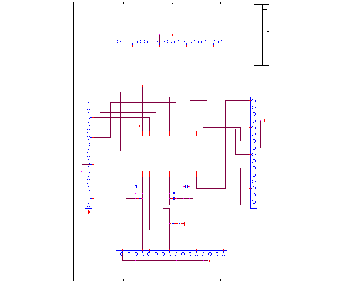
U7
AK4117
R
1
AVDD
2
RX1
3
NC
4
RX0
5
DVDD
6
DVSS
7
XTI
8
XTO
9
LRCK
10
BICK
11
SDTO
12
DAUX
13
MCKO
14
NC
15
UOUT
16
CDTO
17
CDTI
18
CCLK
19
CSN
20
INT1
21
INT0
22
PDN
23
AVSS
24
R61
13k
X1
11.2896MHz
1
2
CN8
1
2
3
4
5
6
7
8
9
10
11
12
13
14
15
16
C22
0.1u
JP19
JMP
C24
5p
+
C21
10u
5
5
4
4
3
3
2
2
1
1
D
D
C
C
B
B
A
A
+5V
VD
DVDD
AVDD
DAUX2
AVDD
DVDD
D3V
VD
D3V
EMCK1
EMCK2
DAUX2
D3V
D3V
D3V
D3V
D3V
D3V
Title
Size
Document Number
R e v
Date:
Sheet
o f
MAIN
0
AKD4117-B
A3
1
2
Friday, December 24, 2004
OPT
BNC
XLR
MCLK
LRCK
SDTO
BICK
GND
GND
GND
L
H
For U1, U2, U5
For U3, U4
AVDD
RX0
RX1
DVDD
PDN
DAUX
MCKO1
BICK
SDTO
LRCK
GND
GND
DAUX
R9
10k
C7
0.1u
R81
47k
R16
100
R8
short
R11
100
R6
short
R82
100
R1
470
U3
74AC245
A0
2
A1
3
A2
4
A3
5
A4
6
A5
7
A6
8
A7
9
B0
18
B1
17
B2
16
B3
15
B4
14
B5
13
B6
12
B7
11
DIR
1
OE
19
GND
10
D3V/VD
20
C4
0.1u
C13
0.1u
R4
short
C16
0.1u
R77
47k
C2
0.1u
R15
100
D1
1S1588
A
K
CN1
1
2
3
4
5
6
7
8
9
10
11
12
13
14
15
16
+
C11
47u
1
2
R20
100
1
2
JP4
R17
100
R21
100
R13
100
R5
75
+
C14
47u
1
2
R12
100
R10
100
R79
47k
U1
74LVC157
D3V
16
GND
8
1Y
4
2Y
7
3Y
9
4Y
12
1A
2
1B
3
2A
5
2B
6
3A
11
3B
10
4A
14
4B
13
G
15
A/B
1
T3
TA48M033F
IN
1
OUT
2
GND
3
CN4
49
50
51
52
53
54
55
56
57
58
59
60
61
62
63
64
JP2
1
3
5
2
4
6
J2
RX0
1
2
3
4
5
PORT1
TORX176
OUT
1
VCC
3
GND
4
GND
2
6
6
5
5
R78
47k
PORT2
DIR
1
2
3
4
5
6
7
8
9
10
C5
0.1u
R19
100
T2
LP2950A
OUT
1
GND
2
IN
3
L1
10u
1
2
R3
short
SW2
PDN
2
1
3
+
C8
10u
1
2
+
C15
47u
1
2
R76
47k
U2A
74HC14
1
2
14
7
R18
100
C3
0.1u
R83
10k
U2B
74HC14
3
4
14
7
C6
0.1u
R80
47k

5
5
4
4
3
3
2
2
1
1
D
D
C
C
B
B
A
A
+5V
VD
D3V
D3V
D3V
Title
Size
Document Number
R e v
Date:
Sheet
o f
MAIN
0
AKD4117-B
A3
2
2
Wednesday, December 22, 2004
CM1/CDTI/SDA
SCL/CCLK
SDA/CDTI
CSN
SDA(ACK)/CDTO
INT0
INT1
CM0/CDTO/CAD1
OCKS1/CCLK/SCL
OCKS0/CSN/CAD0
U
PORT6
uP-I/F
10
8
6
4
2
1
3
5
7
9
R58
10k
LE2
INT1
A
K
+5V
T45_BK
1
R48
10k
U2F
74HC14
13
12
14
7
CN2
17
18
19
20
21
22
23
24
25
26
27
28
29
30
31
32
R49
470
R55
470
U2C
74HC14
5
6
14
7
TP1
U
U2D
74HC14
9
8
14
7
LE1
INT0
A
K
CN3
33
34
35
36
37
38
39
40
41
42
43
44
45
46
47
48
R50
100
R59
100
R60
100
R45
1k
R56
51
R52
470
R51
10k
U5
74LVC157
D3V
16
GND
8
1Y
4
2Y
7
3Y
9
4Y
12
1A
2
1B
3
2A
5
2B
6
3A
11
3B
10
4A
14
4B
13
G
15
A/B
1
R47
1k
R53
100
GND
T45_BK
1
U2E
74HC14
11
10
14
7
R54
10k