 | –≠–ª–µ–∫—Ç—Ä–æ–Ω–Ω—ã–π –∫–æ–º–ø–æ–Ω–µ–Ω—Ç: AKD4368 | –°–∫–∞—á–∞—Ç—å:  PDF PDF  ZIP ZIP |
ASAHI KASEI
[AKD4368-A]
<KM077800>
2005/02
-
1
-
GENERAL DESCRIPTION
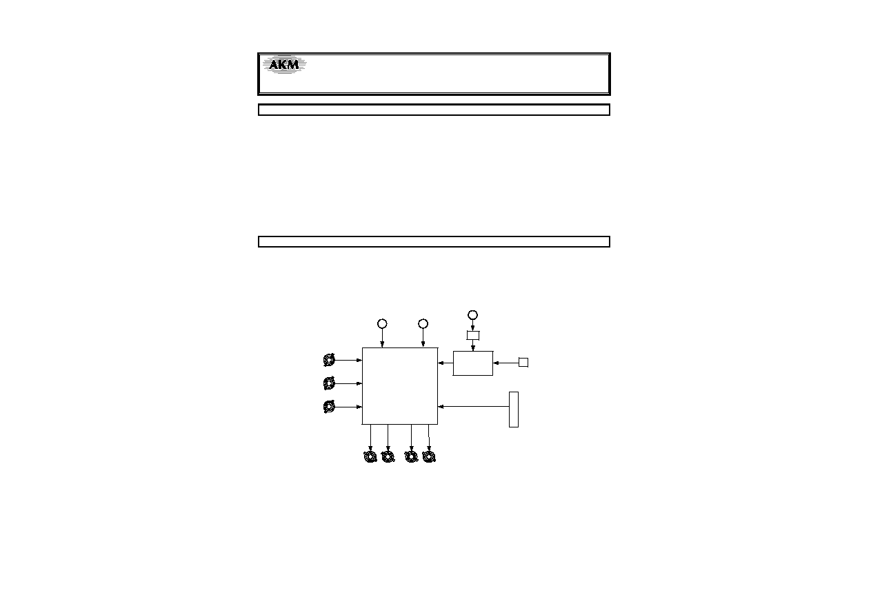
The AKD4368 is an evaluation board for 24bit DAC with built-in Headphone Amplifier, AK4368. The
AKD4368 has the interface with AKM's ADC evaluation boards. Therefore, it's easy to evaluate the
AK4368. The AKD4368 also has the digital audio interface and can achieve the interface with digital audio
systems via opt-connector.
Ordering guide
AKD4368
---
Evaluation
board
for
AK4368
(Cable for connecting with printer port of IBM-AT compatible PC and control
software are packed with this. This control software does not operate on Windows
NT.)
FUNCTION
∑
Compatible with 2 types of interface
- Direct interface with AKM's A/D converter evaluation boards
- On-board AK4114 as DIR which accepts optical input
∑
10pin header for serial control interface
GND
AK4114
(DIR)
Opt In
A/D Data
10pin Header
AK4368
LIN
RIN
MIN
HPL HPR
1.6 ~ 3.6V
LOUT ROUT
Regulator
5.0V
3.0V
Figure 1. AKD4368 Block Diagram
* Circuit diagram and PCB layout are attached at the end of this manual.
Evaluation board Rev.1 for AK4368
AKD4368-A
ASAHI KASEI
[AKD4368-A]
<KM077800>
2005/02
-
2
-
1. Evaluation Board Manual
Operation sequence
1) Set up the power supply lines.
[AVDD]
(orange) =
1.6
3.6V : for AVDD, DVDD and PVDD of AK4368 (typ. 2.4V)
[HVDD]
(orange) =
1.6
3.6V : for HVDD of AK4368 (typ. 2.4V)
[D3V] (orange) = 1.6
3.6V : for 74LVC541 and 74LVC245A (typ. 2.4V)
[VCC] (red) = 5.0V : for logic (typ. 5.0V)
[AGND] (black) = 0V : for analog ground
[DGND] (black) = 0V : for logic ground
Each supply line should be distributed from the power supply unit.
2) Set up the evaluation mode, jumper pins.
(See the followings.)
3) Power on.
The AK4368 and AK4114 should be resets once bringing SW3 (DAC_PDN) and SW2 (DIR_PDN) "L" upon
power-up.
Evaluation mode
In case of the AK4368 evaluation using the AK4114, it is necessary to correspond to audio interface format
for the AK4368 and AK4114. About the AK4368's audio interface format, refer to datasheet of the AK4368.
About the AK4114's audio interface format, refer to Table 2 in this manual.
Applicable Evaluation Mode
(1) PLL Master Mode
(2) PLL Slave Mode
(3) EXT Slave Mode
(3-1) In case of using DIR (Optical Link) <default>
(3-2) In case of connecting AK4368 with a external DSP
(1) PLL Master Mode
PORT3 (ROM) is used. Nothing should be connected to PORT1 (DIR). MCLK, BICK, LRCK and SDATA are
supplied from DSP. It is possible to evaluate at various sampling frequencies using built-in the AK4368's PLL.
AK4368
DSP or
µ
P
MCKO
BICK
LRCK
SDATA
BCLK
LRCK
SDTO
MCKI
1fs
32fs, 64fs
256fs/128fs/64fs/32fs
27MHz,26MHz,19.8MHz,19.68MHz,
19.2MHz,15.36MHz,14.4MHz,13MHz,
12MHz,11.2896MHz
MCLK
Figure 2. PLL Master Mode

ASAHI KASEI
[AKD4368-A]
<KM077800>
2005/02
-
3
-
M/S should be set to "H" for SW1. SDTI,LRCK,BICK of PORT3 should be connected to SDTO,LRCK,BICK
for DSP. In case of supplying MCKO from DSP, the test pin(MCKO)on sub board should be connected to
MCLK of DSP.
The system clock can be supplied by two ways below.
1) Supplied MCKI from J17
JP16
MCLK
JP13
BICK
JP17
EXT
JP12
PHASE
ADC
DIR
MCKO
DI
R
EX
T
INV
THR
JP18
LRCK
ADC
DIR
JP19
SDTI
ADC
DIR
2) Supplied MCKI from MCLK(PORT3)
JP16
MCLK
JP13
BICK
JP17
EXT
JP12
PHASE
ADC
DIR
MCKO
DIR
EXT
INV
THR
JP18
LRCK
ADC
DIR
JP19
SDTI
ADC
DIR
(2) PLL Slave Mode
PORT3 (ROM) is used. BICK,LRCK,SDATA are supplied from DSP. Nothing should be connected to PORT1
(DIR). MCKO is needed for a synchronous singal of BICK and LRCK. M/S should be set to "L" for SW1.
AK4368
DSP or
µ
P
MCKO
BICK
LRCK
SDATA
BCLK
LRCK
SDTO
MCKI
1fs
32fs, 64fs
256fs/128fs/64fs/32fs
27MHz,26MHz,19.8MHz,19.68MHz,
19.2MHz,15.36MHz,14.4MHz,13MHz,
12MHz,11.2896MHz
MCLK
Figure 3. PLL Slave Mode
The test pin (MCKO) on sub board should be connected to MCLK of DSP. System clock MCKI can be
supplied from J17 or PORT3. Setup of jumper pins is same as (1)PLL Master Mode.

ASAHI KASEI
[AKD4368-A]
<KM077800>
2005/02
-
4
-
(3) EXT Slave Mode
AK4368
DSP or
µ
P
MCKI
BICK
LRCK
SDATA
BCLK
LRCK
SDTO
MCKO
1fs
32fs
MCLK
256fs, 512fs or 1024fs
Figure 4. EXT Slave Mode
(3-1)
In case of using DIR (Optical Link) <default>
PORT1 (DIR) is used. DIR generates MCLK, BICK, LRCK and SDATA from the received data through optical
connector (TORX176). Nothing should be connected to PORT3 (DSP) and J17. JP17(EXT)should be short.
CM0 and M/S should be set to "L" for SW1.
JP16
MCLK
JP13
BICK
JP17
EXT
JP12
PHASE
ADC
DIR
MCKO
DIR
EXT
INV
THR
JP18
LRCK
ADC
DIR
JP19
SDTI
ADC
DIR
When the AK4114 is used, JP14 (MKFS) and JP15 (BCFS) are not used. Theerfore, JP14 (MKFS) should be
set to "x1" and JP15 (BCFS) should be set to "64fs".
The AK4114 does not operate under fs = 32kHz. Therefore, this mode corresponds to fs = 32kHz and over.
(3-2) In case of connecting AK4368 with external DSP
PORT3 (ROM) is used. MCLK, BICK, LRCK and SDATA are supplied from PORT3. Nothing should be
connected to PORT1 (DIR). JP17(EXT) should be short.
JP16
MCLK
JP13
BICK
JP17
EXT
JP12
PHASE
ADC
DIR
MCKO
DIR
EXT
INV
THR
JP18
LRCK
ADC
DIR
JP19
SDTI
ADC
DIR
When all interface signals are fed externally, JP14 (MKFS) and JP15 (BCFS) are not used. Therefore, JP14
(MKFS) should be set to "x1" and JP15 (BCFS) should be set to "64fs".
JP12 (PHASE) is jumper which decides polarity of BICK, JP12 should be set to "THR" or "INV" according
to audio interface format.

ASAHI KASEI
[AKD4368-A]
<KM077800>
2005/02
-
5
-
DIP Switch set up
[SW1] : Mode Setting of AK4368 and AK4114
ON is "H", OFF is "L".
No.
Name
ON ("H")
OFF ("L")
1 DIF0
2 DIF2
AK4114 Audio Format Setting
See Table 2
3
CM0
AK4114 X'tal Mode
AK4114 PLL Mode
4 CAD0
5 CAD1
6 I2C
Fixed to "L"
7
M/S
Master mode
Slave mode
Note: M/S is set "H" when PLL, Master Mode
Table 1. Mode Setting for AK4368 and AK4114
Mode
DIF2
DIF0
AK4114 SDTO
0
0
0
16bit, LSB justified
1
0
1
18bit, LSB justified
2
1
0
24bit, MSB justified
(default)
1 1
24bit,
I
2
S
Note: DIF1 is fixed to "L" on the board
Table 2. Setting for AK4114 audio interface format
Other jumper pins set up
1. JP1 (GND) : Analog ground and Digital ground
OPEN :
Separated.
<default>
SHORT : Common. (The connector "DGND" can be open.)
2. JP14 (MKFS) : MCLK Frequency
x1
:
256fs<default>
x2
:
512fs
x4
:
1024fs
3. JP15 (BCFS) : BICK Frequency
32fs
:
32fs
frequency
64fs
:
64fs
frequency<default>
The function of the toggle SW
Upper-side is "H" and lower-side is "L".
[SW2] (DIR): Power down of AK4114. Keep "H" during normal operation.
Keep "L" when the AK4114 is not used.
[SW3] (PDN): Power down of AK4368. Keep "H" during normal operation.
Indication for LED
[LED1] (ERF): Monitor INT0 pin of the AK4114. LED turns on when some error has occurred to AK4114.
ASAHI KASEI
[AKD4368-A]
<KM077800>
2005/02
-
6
-
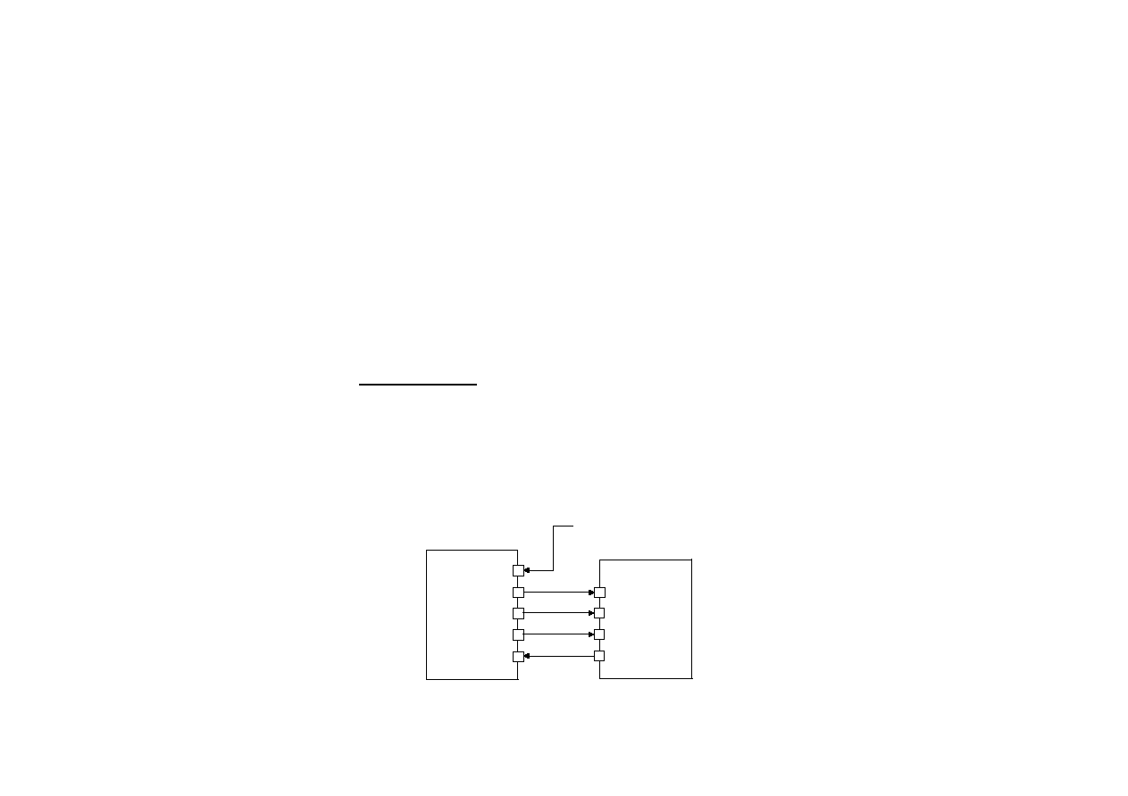
Serial Control
The AK4368 can be controlled via the printer port (parallel port) of IBM-AT compatible PC. Connect PORT4
(CTRL) with PC by 10 wire flat cable packed with the AKD4368.
10pin Header
CSN
10 Wire Flat Cable
CCLK
CDTI
10pin Connector
PC
Connect
AKD4368
Figure 5. Connect of 10 wire flat cable
ASAHI KASEI
[AKD4368-A]
<KM077800>
2005/02
-
7
-
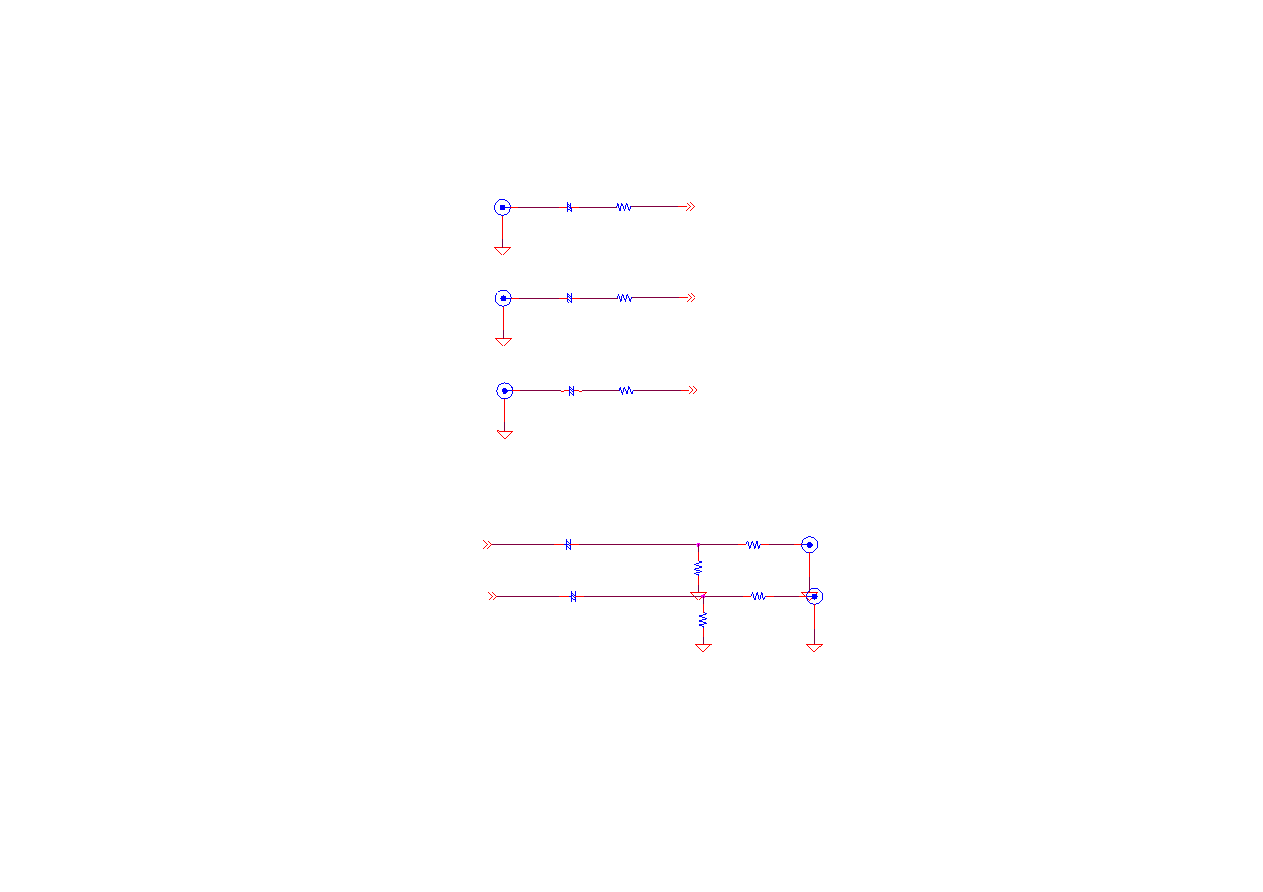
Input / Output circuit & Set-up jumper pin for Input / Output circuits
(1)
Input
Circuit
External analog signal is fed through the BNC connector.
MIN, LIN, RIN Input circuits
Figure 6. MIN, LIN, RIN Input circuits
(2)
Output Circuit
1) LOUT,ROUT Output Circuit
Figure 7. LOUT,RO UT Output Circuit
J7
MIN
+
C26
1u
R18
(SHORT)
MIN
J3
LIN
+
C21
1u
R11
(SHORT)
LIN
J4
RIN
+
C23
1u
R14
(SHORT)
RIN
J14
LOUT
R29
220
LOUT
R30
10k
+
C33
22u
J16
ROUT
R32
220
ROUT
R33
10k
+
C37
22u

ASAHI KASEI
[AKD4368-A]
<KM077800>
2005/02
-
8
-
2) HPL, HPR Output Circuit
Figure 8. HPL, HPR Output Circuit
2)-1. Outputs of HPL and HPR pins are applied via J2 and J8.
JP5
HPR
BNC
HP
JP3
HPL
HP
BNC
2)-2. Outputs of HPL and HPR pins are applied via J5.
JP5
HPR
BNC
HP
JP3
HPL
HP
BNC
* AKM assumes no responsibility for the trouble when using the circuit examples.
1
HP
BNC
+
C22
47u
HPL
HP
R19
(SHORT)
R13
16
HPR
J8
HPR
BNC
J2
HPL
J5
HP
JP5
HPR
R21
16
JP3
HPL
R12
(SHORT)
3
+
C27
47u
2

ASAHI KASEI
[AKD4368-A]
<KM077800>
2005/02
-
9
-
2. Control Software Manual
Set-up of evaluation board and control software
1. Set up the AKD4368 according to previous term.
2. Connect IBM-AT compatible PC with AKD4368 by 10-line type flat cable (packed with AKD4368). Take care of
the direction of 10pin header. (Please install the driver in the CD-ROM when this control software is used on
Windows 2000/XP. Please refer "Installation Manual of Control Software Driver by AKM device control software".
In case of Windows95/98/ME, this installation is not needed. This control software does not operate on Windows
NT.)
3. Insert the CD-ROM labeled "AK4368 Evaluation Kit" into the CD-ROM drive.
4. Access the CD-ROM drive and double-click the icon of "akd4368.exe" to set up the control program.
5. Then please evaluate according to the follows.
Operation flow
Keep the following flow.
1. Set up the control program according to explanation above.
2. Click "Port Reset" button.
3. Click "Write default" button
Explanation of each buttons
1. [Port Reset] : Set up the USB interface board (AKDUSBIF-A) when using the board.
2. [Write default] : Initialize the register of AK4368.
3. [All Write] : Write all registers that is currently displayed.
4. [Function1] : Dialog to write data by keyboard operation.
5. [Function2] : Dialog to write data by keyboard operation.
6. [Function3] : The sequence of register setting can be set and executed.
7. [Function4] : The sequence that is created on [Function3] can be assigned to buttons and executed.
8. [Function5]: The register setting that is created by [SAVE] function on main window can be assigned to
buttons and executed.
9. [SAVE] : Save the current register setting.
10. [OPEN] : Write the saved values to all register.
11. [Write] : Dialog to write data by mouse operation.
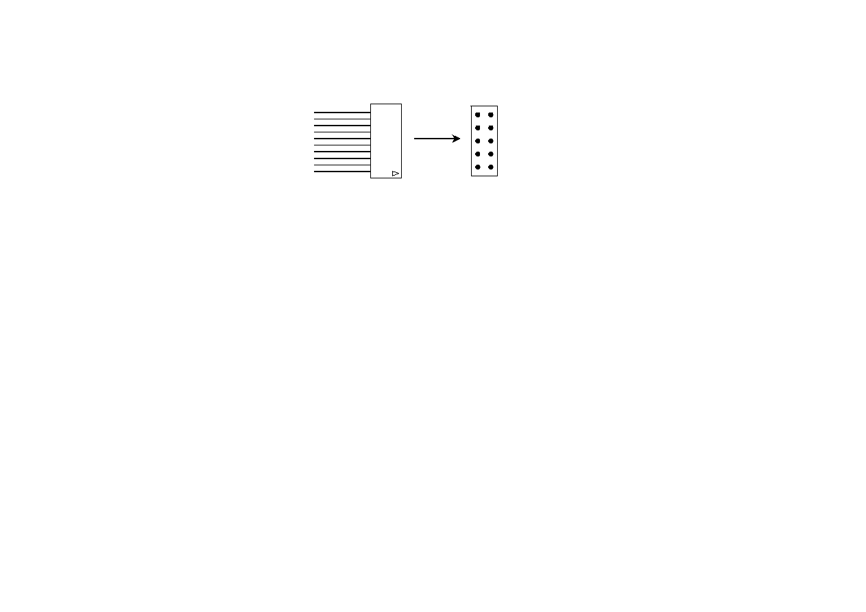
Indication of data
Input data is indicated on the register map. Red letter indicates "H" or "1" and blue one indicates "L" or "0". Blank is the
part that is not defined in the datasheet.

ASAHI KASEI
[AKD4368-A]
<KM077800>
2005/02
-
10
-
Explanation of each dialog
1. [Write
Dialog]
: Dialog to write data by mouse operation
There are dialogs corresponding to each register.
Click the [Write] button corresponding to each register to set up the dialog. If you check the check box, data
becomes "H" or "1". If not, "L" or "0".
If you want to write the input data to AK4368, click [OK] button. If not, click [Cancel] button.
2. [Function1 Dialog]
:
Dialog to write data by keyboard operation
Address Box: Input registers address in 2 figures of hexadecimal.
Data
Box:
Input
registers
data
in
2
figures
of
hexadecimal.
If you want to write the input data to AK4368, click [OK] button. If not, click [Cancel] button.
3. [Function2 Dialog]
:
Dialog to evaluate DATT
There are dialogs corresponding to register of 05h and 06h.
Address Box: Input registers address in 2 figures of hexadecimal.
Start Data Box: Input starts data in 2 figures of hexadecimal.
End Data Box: Input end data in 2 figures of hexadecimal.
Interval Box: Data is written to AK4368 by this interval.
Step Box: Data changes by this step.
Mode Select Box:
If you check this check box, data reaches end data, and returns to start data.
[Example] Start Data = 00, End Data = 09
Data flow: 00 01 02 03 04 05 06 07 08 09 09 08 07 06 05 04 03 02 01 00
If you do not check this check box, data reaches end data, but does not return to start data.
[Example] Start Data = 00, End Data = 09
Data flow: 00 01 02 03 04 05 06 07 08 09
If you want to write the input data to AK4368, click [OK] button. If not, click [Cancel] button.

ASAHI KASEI
[AKD4368-A]
<KM077800>
2005/02
-
11
-
4. [SAVE] and [OPEN]
4-1. [SAVE]
All of current register setting values displayed on the main window are saved to the file. The extension of file name is
"akr".
<Operation flow>
(1) Click [SAVE] Button.
(2) Set the file name and click [SAVE] Button. The extension of file name is "akr".
4-2. [OPEN]
The register setting values saved by [SAVE] are written to the AK4368. The file type is the same as [SAVE].
<Operation flow>
(1) Click [OPEN] Button.
(2) Select the file (*.akr) and Click [OPEN] Button.

ASAHI KASEI
[AKD4368-A]
<KM077800>
2005/02
-
12
-
5. [Function3 Dialog]
The sequence of register setting can be set and executed.
(1) Click [F3] Button. The default setting sequence DAC->HP(3D=OFF) is displayed. Jump to (3) below if the default
setting sequence is used. Go to (2) if the other setting sequence is required.
(2) Set the control sequence.
Set the address, Data and Interval time. Set "-1" to the address of the step where the sequence should be paused.
(3) Click [START] button. Then this sequence is executed.
The sequence is paused at the step of Interval="-1". Click [START] button, the sequence restarts from the paused step.
This sequence can be saved and opened by [SAVE] and [OPEN] button on the Function3 window. The extension of file
name is "aks".
Figure 9. Window of [F3]
ASAHI KASEI
[AKD4368-A]
<KM077800>
2005/02
-
13
-
6. [Function4 Dialog]
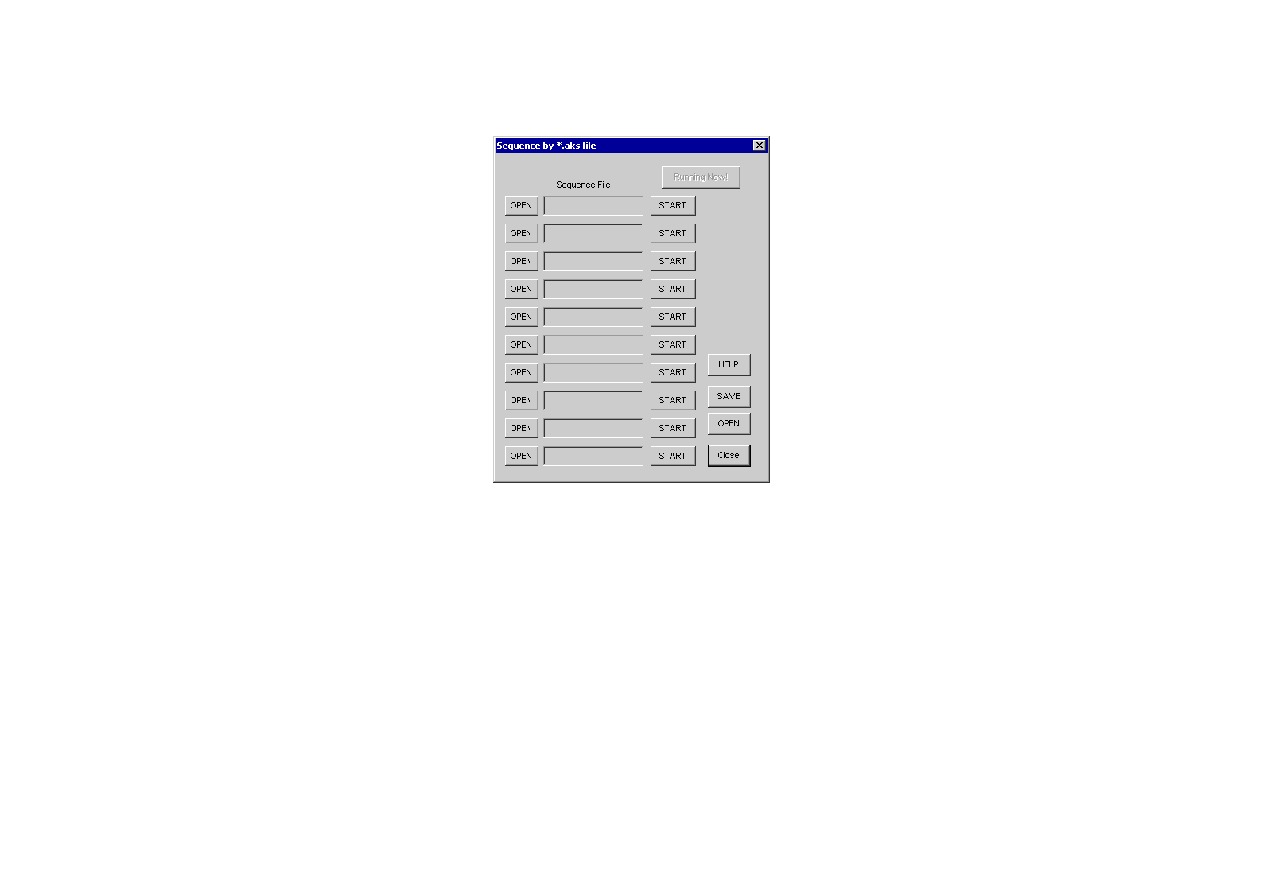
The sequence file (*.aks) saved by [Function3] can be listed up to 10 files, assigned to buttons and then executed.
When [F4] button is clicked, the window as shown in Figure 10 opens.
Figure 10. [F4] window

ASAHI KASEI
[AKD4368-A]
<KM077800>
2005/02
-
14
-
6-1. [OPEN] buttons on left side and [START] buttons
(1) Click [OPEN] button and select the sequence file (*.aks) saved by [Function3].
The sequence file name is displayed as shown in Figure 11. ( In case that the selected sequence file name is
"DAC_Stereo_ON.aks")
Figure 11. [F4] window(2)
(2) Click [START] button, then the sequence is executed.
6-2. [SAVE] and [OPEN] buttons on right side
[SAVE] : The name assign of sequence file displayed on [Function4] window can be saved to the file. The file name
is "*.ak4".
[OPEN] : The name assign of sequence file(*.ak4) saved by [SAVE] is loaded.
6-3. Note
(1) This function doesn't support the pause function of sequence function.
(2) All files used by [SAVE] and [OPEN] function on right side need to be in the same folder.
(3) When the sequence is changed in [Function3], the sequence file (*.aks) should be loaded again in order to reflect the
change.

ASAHI KASEI
[AKD4368-A]
<KM077800>
2005/02
-
15
-
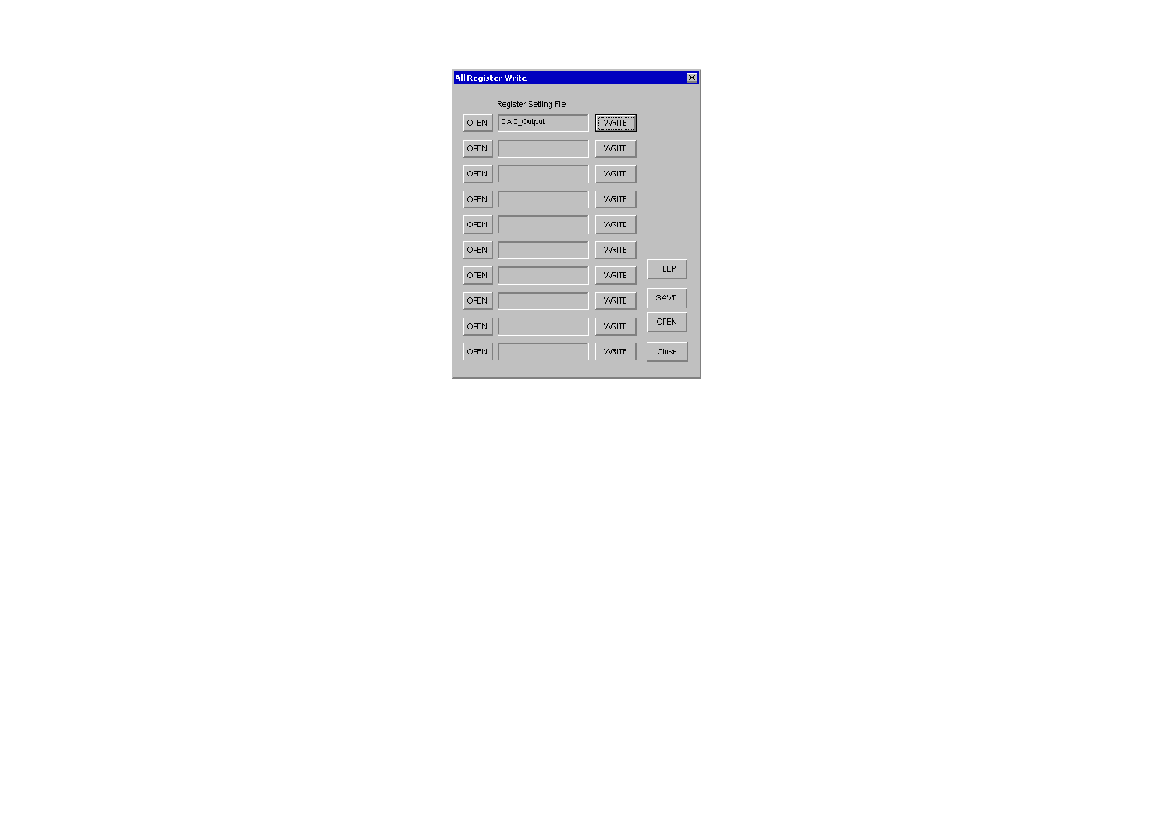
7. [Function5 Dialog]
The register setting file(*.akr) saved by [SAVE] function on main window can be listed up to 10 files, assigned to
buttons and then executed.
When [F5] button is clicked, the window as shown in Figure 12 opens.
Figure 12. [F5] window
7-1. [OPEN] buttons on left side and [WRITE] button
(1) Click [OPEN] button and select the register setting file (*.akr).
The register setting file name is displayed as shown in Figure 13. (In case that the selected file name is
"DAC_Output.akr")
(2) Click [WRITE] button, then the register setting is executed.
ASAHI KASEI
[AKD4368-A]
<KM077800>
2005/02
-
16
-
Figure 13. [F5] windows(2)
7-2. [SAVE] and [OPEN] buttons on right side
[SAVE] : The name assign of register setting file displayed on [Function5] window can be saved to the file. The file
name is "*.ak5".
[OPEN] : The name assign of register setting file(*.ak5) saved by [SAVE] is loaded.
7-3. Note
(1) All files used by [SAVE] and [OPEN] function on right side need to be in the same folder.
(2) When the register setting is changed by [SAVE] Button on the main window, the register setting file (*.akr) should be
loaded again in order to reflect the change.

ASAHI KASEI
[AKD4368-A]
<KM077800>
2005/02
-
17
-
MEASUREMENT RESULTS
[Measurement condition]
∑ Measurement unit : Audio Precession System Two Cascade
∑
MCLK :
11.2896MHz
∑
BICK
:
64fs
∑
fs :
44.1kHz
∑
Bit
:
24bit
∑ Measurement mode : EXT Slave mode
∑ Power Supply : VDD = HVDD = 3.3V
∑ Measurement Filter : 10Hz 20kHz
∑ Temperature : Room
Parameter DAC Analog Output Characteristics
Result (Lch / Rch)
Unit
DAC -> HPAMP
THD+N (-3dBFS Output)
-56.5 / -57.0
dB
D-Range (-60dB Output, A-weighted)
90.7 / 90.7
dB
S/N (A-weighted)
90.8 / 90.8
dB
DAC -> LOUT
THD+N (0dBFS Output)
-75.8 / -75.7
dB
D-Range (-60dB Output, A-weighted)
88.7 / 88.4
dB
S/N (A-weighted)
88.7 / 88.4
dB

ASAHI KASEI
[AKD4368-A]
<KM077800>
2005/02
-
18
-
[Plot of Headphone Amp]
AKM
AK4368 HP-AMP THD+N vs. Input Level (fs= 44.1kHz, fin= 1kHz)
-100
-20
-95
-90
-85
-80
-75
-70
-65
-60
-55
-50
-45
-40
-35
-30
-25
d
B
r
A
-140
+0
-130
-120
-110
-100
-90
-80
-70
-60
-50
-40
-30
-20
-10
dBFS
Figure 14. THD+N vs. Input Level
AKM
AK4368 HP-AMP THD+N vs. Input Frequency (fs= 44.1kHz, fin= 1kHz)
-100
-20
-95
-90
-85
-80
-75
-70
-65
-60
-55
-50
-45
-40
-35
-30
-25
d
B
r
A
20
20k
50
100
200
500
1k
2k
5k
10k
Hz
Figure 15. THD+N vs. Input Frequency

ASAHI KASEI
[AKD4368-A]
<KM077800>
2005/02
-
19
-
AKM
AK4368 HP-AMP Linearity (fs= 44.1kHz, fin= 1kHz)
-140
+0
-130
-120
-110
-100
-90
-80
-70
-60
-50
-40
-30
-20
-10
d
B
r
A
-140
+0
-130
-120
-110
-100
-90
-80
-70
-60
-50
-40
-30
-20
-10
dBFS
Figure 16. Linearity
AKM
AK4368 HP-AMP Freq response(fs= 44.1kHz, Input Level= -3dB)
-24
-0
-22
-20
-18
-16
-14
-12
-10
-8
-6
-4
-2
d
B
r
A
20
20k
50
100
200
500
1k
2k
5k
10k
Hz
Figure 17. Frequency Response (Boost off)
(including external HPF)

ASAHI KASEI
[AKD4368-A]
<KM077800>
2005/02
-
20
-
AKM
AK4368 HP-AMP FFT(fs=44.1kHz, fin=1kHz, Input Level = -3dB)
-160
+0
-150
-140
-130
-120
-110
-100
-90
-80
-70
-60
-50
-40
-30
-20
-10
d
B
r
A
20
20k
50
100
200
500
1k
2k
5k
10k
Hz
Figure 18. FFT Plot(1kHz,-3dB)
AKM
AK4368 HP-AMP FFT(fs=44.1kHz, fin=1kHz, Input Level = -60dB)
-160
+0
-150
-140
-130
-120
-110
-100
-90
-80
-70
-60
-50
-40
-30
-20
-10
d
B
r
A
20
20k
50
100
200
500
1k
2k
5k
10k
Hz
Figure 19. FFT Plot(1kHz,-3dB)

ASAHI KASEI
[AKD4368-A]
<KM077800>
2005/02
-
21
-
AKM
AK4368 HP-AMP Noise Floor (No data Input)
-160
+0
-150
-140
-130
-120
-110
-100
-90
-80
-70
-60
-50
-40
-30
-20
-10
d
B
r
A
20
20k
50
100
200
500
1k
2k
5k
10k
Hz
Figure 20. FFT Plot(Noise Floor)
AKM
AK4368 HP-AMP FFT Out-of-band Noise
-160
+0
-150
-140
-130
-120
-110
-100
-90
-80
-70
-60
-50
-40
-30
-20
-10
d
B
r
A
20
100k
50
100
200
500
1k
2k
5k
10k
20k
50k
Hz
Figure 21. Out-band Noise

ASAHI KASEI
[AKD4368-A]
<KM077800>
2005/02
-
22
-
AKM
AK
4368
HP-AMP Crosstalk (fs= 44.1kHz, Input level= -3dB)
Upper@1kHz:Rch-->Lch; Lower@1kHz:Lch-->Rch
-
120
+
0
-
110
-
100
-
90
-
80
-
70
-
60
-
50
-
40
-
30
-
20
-
10
d
B
20
20k
50
100
200
500
1k
2k
5
k
10
k
Hz
Figure 22. Crosstalk
IMPORTANT NOTICE
∑
These products and their specifications are subject to change without notice. Before considering
any use or application, consult the Asahi Kasei Microsystems Co., Ltd. (AKM) sales office or
authorized distributor concerning their current status.
∑
AKM assumes no liability for infringement of any patent, intellectual property, or other right in the
application or use of any information contained herein.
∑
Any export of these products, or devices or systems containing them, may require an export license
or other official approval under the law and regulations of the country of export pertaining to customs
and tariffs, currency exchange, or strategic materials.
∑
AKM products are neither intended nor authorized for use as critical components in any safety, life
support, or other hazard related device or system, and AKM assumes no responsibility relating to
any such use, except with the express written consent of the Representative Director of AKM. As
used here:
(a) A hazard related device or system is one designed or intended for life support or maintenance of
safety or for applications in medicine, aerospace, nuclear energy, or other fields, in which its
failure to function or perform may reasonably be expected to result in loss of life or in significant
injury or damage to person or property.
(b) A critical component is one whose failure to function or perform may reasonably be expected to
result, whether directly or indirectly, in the loss of the safety or effectiveness of the device or
system containing it, and which must therefore meet very high standards of performance and
reliability.
∑ It is the responsibility of the buyer or distributor of an AKM product who distributes, disposes of, or otherwise places the product with
a third party to notify that party in advance of the above content and conditions, and the buyer or distributor agrees to assume any and
all responsibility and liability for and hold AKM harmless from any and all claims arising from the use of said product in the absence
of such notification.

A
A
B
B
C
C
D
D
E
E
E
E
D
D
C
C
B
B
A
A
HVDD
AVDD
LIN
RIN
MI
N
4368_BICK
4368_LRCK
4368_SDATA
SCL/CCLK
CAD0/CSN
DVDD
DVDD
HPL
HPR
4368_M
CKO
4368_PDN
SDA/CDTI
LO
UT
ROUT
4368_I2C
EXT_MCLK
SDTO
CDTO
Title
Size
Document Number
Rev
Date:
Sheet
of
AK4368
A
AKD4368-A Rev.0
A3
1
6
Friday, January 07, 2005
Title
Size
Document Number
Rev
Date:
Sheet
of
AK4368
A
AKD4368-A Rev.0
A3
1
6
Friday, January 07, 2005
Title
Size
Document Number
Rev
Date:
Sheet
of
AK4368
A
AKD4368-A Rev.0
A3
1
6
Friday, January 07, 2005
DGND
AGND
+
C12
10u
+
C12
10u
1
TP29
3DCAP3
TP29
3DCAP3
R5
10k
R5
10k
1
TP17
AVSS
TP17
AVSS
1
2
L1
(short)
L1
(short)
1
TP22
ROUT
TP22
ROUT
1
TP27
3DCAP1
TP27
3DCAP1
1
2
L2
(short)
L2
(short)
1
TP4
PDN
TP4
PDN
1
TP3
DVSS
TP3
DVSS
1
TP5
CAD0/CSN
TP5
CAD0/CSN
C11
0.1u
C11
0.1u
1
TP25
VCOC
TP25
VCOC
1
TP24
RIN
TP24
RIN
C14
470n
C14
470n
+
C9
10u
+
C9
10u
C17(open)
C17(open)
R6
51
R6
51
1
2
3
4
5
6
7
8
9
10
11
12
CN2
CN2
1
TP15
VCOM
TP15
VCOM
1
TP11
BICK
TP11
BICK
C6
0.1u
C6
0.1u
+
C3
1u
+
C3
1u
1
TP16
HVDD
TP16
HVDD
1
TP9
SDATA
TP9
SDATA
37
38
39
40
41
42
43
44
45
46
47
48
CN1
CN1
13
14
15
16
17
18
19
20
21
22
23
24
CN4
CN4
1
TP14
MCKI
TP14
MCKI
C15
4.7n
C15
4.7n
JP1
GND
JP1
GND
1
TP28
3DCAP2
TP28
3DCAP2
1
TP6
SCL/CCLK
TP6
SCL/CCLK
C10
4.7n
C10
4.7n
R4
51
R4
51
1
TP26
LIN
TP26
LIN
NC
A1
MCKO
B1
DVSS
C2
DVDD
C1
MCKI
D1
I2C
D2
BICK
E1
LRCK
E2
SDA/CDTI
F1
SDATA
F2
NC
G1
S
C
L/
CCLK
G2
NC
F3
CA
D0/
C
S
N
G3
PD
N
F4
NC
G4
NC
F5
3
D
C
AP1
G5
3
D
C
AP2
F6
3
D
C
AP3
G6
LOUT
F7
ROUT
E6
NC
G7
VCOM
E7
AVDD
D7
MUTET
D6
HVDD
C7
AVSS
C6
HVSS
B6
HPR
B7
NC
A7
NC
B5
HP
L
A6
MIN
A5
NC
B4
RI
N
A4
VC
O
C
A3
LI
N
B3
PVSS
B2
PVD
D
A2
NC
C3
U1
AK4368
U1
AK4368
1
TP2
PVDD
TP2
PVDD
C2
0.1u
C2
0.1u
1
TP23
MIN
TP23
MIN
R3
10
R3
10
1
TP18
HVSS
TP18
HVSS
R7
(short)
R7
(short)
1
TP13
DVDD
TP13
DVDD
+
C16
10u
+
C16
10u
1
TP21
LOUT
TP21
LOUT
C4
0.1u
C4
0.1u
+
C1
10u
+
C1
10u
1
2
+
C13
47u
+
C13
47u
1
TP7
SDA/CDTI
TP7
SDA/CDTI
R1
51
R1
51
1
TP8
I2C
TP8
I2C
R2
51
R2
51
1
TP12
MCKO
TP12
MCKO
25
26
27
28
29
30
31
32
33
34
35
36
CN3
CN3
1
TP20
HPL
TP20
HPL
1
TP19
HPR
TP19
HPR
1
TP10
LRCK
TP10
LRCK
1
2
+
C7
47u
+
C7
47u
+
C5
2.2u
+
C5
2.2u
C8
0.1u
C8
0.1u
1
TP1
AVDD
TP1
AVDD

A
A
B
B
C
C
D
D
E
E
E
E
D
D
C
C
B
B
A
A
LIN
RIN
MIN
HPR
HPL
LOUT
ROUT
Title
Size
Document Number
Rev
Date:
Sheet
of
Input/Output
A
AKD4368-A Rev.0
A3
2
6
Friday, December 24, 2004
Title
Size
Document Number
Rev
Date:
Sheet
of
Input/Output
A
AKD4368-A Rev.0
A3
2
6
Friday, December 24, 2004
Title
Size
Document Number
Rev
Date:
Sheet
of
Input/Output
A
AKD4368-A Rev.0
A3
2
6
Friday, December 24, 2004
HP
BNC
HP
BNC
J2
HPL
J2
HPL
R33
10k
R33
10k
R13
16
R13
16
R19
6.8
R19
6.8
R14(short)
R14(short)
+
C33
22u
+
C33
22u
J3
LIN
J3
LIN
R12
6.8
R12
6.8
JP3
HPL
JP3
HPL
J16
ROUT
J16
ROUT
R18(short)
R18(short)
+
C22
47u
+
C22
47u
R29
220
R29
220
J8
HPR
J8
HPR
+
C21
1u
+
C21
1u
J4
RIN
J4
RIN
+
C37
22u
+
C37
22u
R11(short)
R11(short)
R32
220
R32
220
JP5
HPR
JP5
HPR
J7
MIN
J7
MIN
R30
10k
R30
10k
J5
HP
J5
HP
+
C23
1u
+
C23
1u
+
C27
47u
+
C27
47u
J14
LOUT
J14
LOUT
+
C26
1u
+
C26
1u
R21
16
R21
16

A
A
B
B
C
C
D
D
E
E
E
E
D
D
C
C
B
B
A
A
VCC
VCC
EXT_MCLK
X_LRCK
DIR_MCLK
MCKO
EXT_BICK
BICK
DIR_BICK
Title
Size
Document Number
Rev
Date:
Sheet
of
CLOCK
A
AKD4368-A Rev.0
A3
3
6
Friday, December 24, 2004
Title
Size
Document Number
Rev
Date:
Sheet
of
CLOCK
A
AKD4368-A Rev.0
A3
3
6
Friday, December 24, 2004
Title
Size
Document Number
Rev
Date:
Sheet
of
CLOCK
A
AKD4368-A Rev.0
A3
3
6
Friday, December 24, 2004
EXT
DIR
MCKO
x4
64fs
x2
x1
32fs
INV
THR
DIR
ADC
D
2
CLK
3
Q
5
Q
6
PR
4
CL
1
U4A
74AC74
U4A
74AC74
R35
51
R35
51
1
2
U2A
74HC14
U2A
74HC14
JP16
MCLK
JP16
MCLK
J17
EXT
J17
EXT
JP13
BICK
JP13
BICK
D
12
CLK
11
Q
9
Q
8
PR
10
CL
13
U4B
74AC74
U4B
74AC74
JP14
MKFS
JP14
MKFS
JP17
EXT
JP17
EXT
CLK
10
RST
11
Q1
9
Q2
7
Q3
6
Q4
5
Q5
3
Q6
2
Q7
4
Q8
13
Q9
12
Q10
14
Q11
15
Q12
1
U3
74HC4040
U3
74HC4040
JP12
PHASE
JP12
PHASE
JP15
BCFS
JP15
BCFS

A
A
B
B
C
C
D
D
E
E
E
E
D
D
C
C
B
B
A
A
VCC
VCC
VCC
VCC
VCC
VCC
VCC
SDTO
DIR_SDTI
DIR_BICK
DIR_LRCK
DIR_MCLK
CAD0
CM0
CM0
REG
REG
DAUX
REG
CAD1
I2C
M/S
Title
Size
Document Number
Rev
Date:
Sheet
of
DIR/DIT
A
AKD4368-A Rev.0
A3
4
6
Friday, December 24, 2004
Title
Size
Document Number
Rev
Date:
Sheet
of
DIR/DIT
A
AKD4368-A Rev.0
A3
4
6
Friday, December 24, 2004
Title
Size
Document Number
Rev
Date:
Sheet
of
DIR/DIT
A
AKD4368-A Rev.0
A3
4
6
Friday, December 24, 2004
H
L
DIF0
DIF2
CAD0
CM0
for 74AC74, 74HC4040, 74HC14,
74HCT157, 74LS07, 74HCT04
CAD1
I2C
M/S
C45
0.1u
C45
0.1u
+
C48
10u
+
C48
10u
3
4
U2B
74HC14
U2B
74HC14
C51
0.47u
C51
0.47u
C43
0.1u
C43
0.1u
R38
1k
R38
1k
R39
10k
R39
10k
C44
0.1u
C44
0.1u
1
2
L4
47u
L4
47u
C46
0.1u
C46
0.1u
1
2
U6A
74HCT04
U6A
74HCT04
OUT
1
VCC
3
GND
4
GND
2
6
6
5
5
PORT1
DIR
PORT1
DIR
GND
1
IF
2
VCC
3
IN
4
5
5
6
6
PORT2
DIT
PORT2
DIT
+
C57
10u
+
C57
10u
C54
5p
C54
5p
C50
0.1u
C50
0.1u
C40
0.1u
C40
0.1u
C41
0.1u
C41
0.1u
2
1
LED1
ERF
LED1
ERF
7
6
5
4
3
2
1
RP1
47k
RP1
47k
C55
0.1u
C55
0.1u
3
4
U6B
74HCT04
U6B
74HCT04
R40
1k
R40
1k
C56
0.1u
C56
0.1u
+
C49
10u
+
C49
10u
C42
0.1u
C42
0.1u
C47
0.1u
C47
0.1u
VIN
2
VOUT
3
GND
1
T1
TO92
T1
TO92
C53
0.1u
C53
0.1u
1
2
3
4
5
6
7
14
13
12
11
10
9
8
SW1
MODE
SW1
MODE
+
C38
47u
+
C38
47u
1
2
X2
11.2896MHz
X2
11.2896MHz
5
6
U6C
74HCT04
U6C
74HCT04
C52
5p
C52
5p
5
6
U2C
74HC14
U2C
74HC14
1
2
L3
10u
L3
10u
R36
470
R36
470
2
1
3
SW2
DIR
SW2
DIR
C39
0.1u
C39
0.1u
C59
0.1u
C59
0.1u
IPS0
1
NC
2
DIF0
3
TEST2
4
DIF1
5
NC
6
DIF2
7
IPS1
8
P/SN
9
XTL0
10
XTL1
11
TVD
D
13
D
VSS
14
TX0
15
TX1
16
BO
U
T
17
COUT
18
UOUT
19
VO
U
T
20
DV
DD
21
D
VSS
22
MC
KO1
23
BICK
26
MCKO2
27
DAUX
28
XTO
29
XTI
30
PDN
31
CM0
32
CM1
33
OCKS1
34
OCKS0
35
INT0
36
AVD
D
38
R
39
VC
O
M
40
AVSS
41
RX
0
42
NC
43
RX
1
44
TEST1
45
RX
2
46
NC
47
RX
3
48
VIN
12
LRCK
24
SDTO
25
IN
T1
37
U5
AK4114
U5
AK4114
2
1
D1
HSU119
D1
HSU119
+
C58
10u
+
C58
10u
R37
18k
R37
18k

A
A
B
B
C
C
D
D
E
E
E
E
D
D
C
C
B
B
A
A
D3V
VCC
VCC
VCC
D3V
4368_PDN
CAD0/CSN
SCL/CCLK
4368_SDATA
4368_I2C
4368_LRCK
4368_BICK
D3V
D3V
DAUX
BICK
DIR_SDTI
EXT_MCLK
EXT_BICK
DIR_LRCK
X_LRCK
4368_MCKO
M/S
MCKO
CDTO
SDA/CDTI
CAD1
I2C
I2C
CAD0
Title
Size
Document Number
Rev
Date:
Sheet
of
LOGIC
A
AKD4368-A Rev.0
A3
5
6
Friday, December 24, 2004
Title
Size
Document Number
Rev
Date:
Sheet
of
LOGIC
A
AKD4368-A Rev.0
A3
5
6
Friday, December 24, 2004
Title
Size
Document Number
Rev
Date:
Sheet
of
LOGIC
A
AKD4368-A Rev.0
A3
5
6
Friday, December 24, 2004
LRCK
ADC
ADC
DIR
MCLK
VCC
SDTI
DIR
BICK
SCL/CCLK
CDTO/SDA(ACK)
SDA/CDTI
CSN
L
H
JP19
SDTI
JP19
SDTI
6
5
4
3
2
1
RP2
47k
RP2
47k
9
8
U2D
74HC14
U2D
74HC14
R42 51
R42 51
JP18
LRCK
JP18
LRCK
R41 51
R41 51
A1
2
A2
3
A4
5
A5
6
A6
7
A7
8
A8
9
DIR
1
G
19
B1
18
B2
17
B3
16
B4
15
B5
14
B6
13
B7
12
B8
11
VCC
20
GND
10
A3
4
U7
74ALVC245
U7
74ALVC245
6
5
4
3
2
1
RP3
47k
RP3
47k
R48
10k
R48
10k
2
1
3
SW3
PDN
SW3
PDN
R46
10k
R46
10k
C61
0.1u
C61
0.1u
1A
2
1B
3
2A
5
2B
6
3A
11
3B
10
4A
14
4B
13
A/B
1
G
15
1Y
4
2Y
7
3Y
9
4Y
12
U9
74HCT157
U9
74HCT157
R45
470
R45
470
C60
0.1u
C60
0.1u
1
2
U10A
74LS07
U10A
74LS07
R50
10k
R50
10k
1
2
3
4
5
6
7
8
9
10
PORT3
ROM
PORT3
ROM
+
C62
47u
+
C62
47u
R51
1.8k
R51
1.8k
11
10
U2E
74HC14
U2E
74HC14
R49
470
R49
470
R43
10k
R43
10k
A1
2
A2
3
A3
4
A4
5
A5
6
A6
7
A7
8
A8
9
G1
1
G2
19
Y1
18
Y2
17
Y3
16
Y4
15
Y5
14
Y6
13
Y7
12
Y8
11
VCC
20
GND
10
U8
74LVC541
U8
74LVC541
C63
0.1u
C63
0.1u
R44
10k
R44
10k
2
1
D2
HSU119
D2
HSU119
R47
470
R47
470
R52
51
R52
51
1
2
3
4
5
6
7
8
9
10
PORT4
CTRL
PORT4
CTRL

A
A
B
B
C
C
D
D
E
E
E
E
D
D
C
C
B
B
A
A
Title
Size
Document Number
Rev
Date:
Sheet
of
PIN
A
AKD4638-A Rev.0
A3
6
6
Friday, December 24, 2004
Title
Size
Document Number
Rev
Date:
Sheet
of
PIN
A
AKD4638-A Rev.0
A3
6
6
Friday, December 24, 2004
Title
Size
Document Number
Rev
Date:
Sheet
of
PIN
A
AKD4638-A Rev.0
A3
6
6
Friday, December 24, 2004
11
10
U6E
74HCT04
U6E
74HCT04
5
6
U10C
74LS07
U10C
74LS07
13
12
U10F
74LS07
U10F
74LS07
9
8
U10D
74LS07
U10D
74LS07
9
8
U6D
74HCT04
U6D
74HCT04
13
12
U6F
74HCT04
U6F
74HCT04
11
10
U10E
74LS07
U10E
74LS07
13
12
U2F
74HC14
U2F
74HC14
3
4
U10B
74LS07
U10B
74LS07

A
A
B
B
C
C
D
D
E
E
E
E
D
D
C
C
B
B
A
A
Title
Size
Document Number
Rev
Date:
Sheet
of
AK4368
A
AK4368-SUB for 41BGA
A3
1
6
Friday, January 07, 2005
Title
Size
Document Number
Rev
Date:
Sheet
of
AK4368
A
AK4368-SUB for 41BGA
A3
1
6
Friday, January 07, 2005
Title
Size
Document Number
Rev
Date:
Sheet
of
AK4368
A
AK4368-SUB for 41BGA
A3
1
6
Friday, January 07, 2005
1
TP7
SDA/CDTI
TP7
SDA/CDTI
+
C1
10u
+
C1
10u
R17
10k
R17
10k
1
TP4
PDN
TP4
PDN
C2
0.1u
C2
0.1u
1
TP29
3DCAP3
TP29
3DCAP3
37
38
39
40
41
42
43
44
45
46
47
48
CN1
CN1
C6
0.1u
C6
0.1u
1
TP2
PVDD
TP2
PVDD
1
TP27
3DCAP1
TP27
3DCAP1
C11
0.1u
C11
0.1u
NC
A1
MCKO
B1
DVSS
C2
DVDD
C1
MCKI
D1
I2C
D2
BICK
E1
LRCK
E2
SDA/CDTI
F1
SDATA
F2
NC
G1
S
C
L/
CCLK
G2
NC
F3
CA
D0/
C
S
N
G3
PD
N
F4
NC
G4
NC
F5
3
D
C
AP1
G5
3
D
C
AP2
F6
3
D
C
AP3
G6
LOUT
F7
ROUT
E6
NC
G7
VCOM
E7
AVDD
D7
MUTET
D6
HVDD
C7
AVSS
C6
HVSS
B6
HPR
B7
NC
A7
NC
B5
HP
L
A6
MIN
A5
NC
B4
RI
N
A4
VC
O
C
A3
LI
N
B3
PVSS
B2
PVD
D
A2
NC
C3
U1
AK4368
U1
AK4368
1
TP6
SCL/CCLK
TP6
SCL/CCLK
+
C12
10u
+
C12
10u
C4
0.1u
C4
0.1u
R4
51
R4
51
1
TP13
DVDD
TP13
DVDD
13
14
15
16
17
18
19
20
21
22
23
24
CN4
CN4
1
TP22
ROUT
TP22
ROUT
R7
(short)
R7
(short)
1
TP20
HPL
TP20
HPL
1
TP9
SDATA
TP9
SDATA
1
TP23
MIN
TP23
MIN
1
2
3
4
5
6
7
8
9
10
11
12
CN2
CN2
1
TP8
I2C
TP8
I2C
1
TP11
BICK
TP11
BICK
1
TP5
CAD0/CSN
TP5
CAD0/CSN
1
TP17
AVSS
TP17
AVSS
R6
51
R6
51
1
TP16
HVDD
TP16
HVDD
1
TP25
VCOC
TP25
VCOC
+
C9
10u
+
C9
10u
1
TP14
MCKI
TP14
MCKI
R1
51
R1
51
C15
4.7n
C15
4.7n
C8
0.1u
C8
0.1u
+
C16
10u
+
C16
10u
C17(open)
C17(open)
+
C5
2.2u
+
C5
2.2u
1
TP18
HVSS
TP18
HVSS
1
TP15
VCOM
TP15
VCOM
1
TP1
AVDD
TP1
AVDD
1
TP10
LRCK
TP10
LRCK
1
TP12
MCKO
TP12
MCKO
1
TP19
HPR
TP19
HPR
1
TP28
3DCAP2
TP28
3DCAP2
C14
470n
C14
470n
R2
51
R2
51
+
C46
1u
+
C46
1u
1
TP3
DVSS
TP3
DVSS
C10
4.7n
C10
4.7n
25
26
27
28
29
30
31
32
33
34
35
36
CN3
CN3
1
TP24
RIN
TP24
RIN
1
TP26
LIN
TP26
LIN
1
TP21
LOUT
TP21
LOUT


