 | –≠–ª–µ–∫—Ç—Ä–æ–Ω–Ω—ã–π –∫–æ–º–ø–æ–Ω–µ–Ω—Ç: AKD4384 | –°–∫–∞—á–∞—Ç—å:  PDF PDF  ZIP ZIP |

ASAHI KASEI
[AK4384]
MS0176-E-00
2002/09
- 1 -
GENERAL DESCRIPTION
The AK4384 offers the perfect mix for cost and performance based audio systems. Using AKM's multi bit
architecture for its modulator the AK4384 delivers a wide dynamic range while preserving linearity for
improved THD+N performance. The AK4384 integrates a combination of SCF and CTF filters increasing
performance for systems with excessive clock jitter. The 24 Bit word length and 192kHz sampling rate
make this part ideal for a wide range of applications including DVD-Audio. The AK4384 is offered in a
space saving 16pin TSSOP package.
FEATURES
o
Sampling Rate Ranging from 8kHz to 192kHz
o
128 times Oversampling (Normal Speed Mode)
o
64 times Oversampling (Double Speed Mode)
o
32 times Oversampling (Quad Speed Mode)
o
24-Bit 8 times FIR Digital Filter
o
SCF with High Tolerance to Clock Jitter
o
2nd order Analog LPF
o
Single Ended Output Buffer
o
Digital de-emphasis for 32k, 44.1k and 48kHz sampling
o
Soft mute
o
Digital Attenuator (Linear 256 steps)
o
I/F format: 24-Bit MSB justified, 24/20/16-Bit LSB justified or I
2
S
o
Master clock: 256fs, 384fs, 512fs, 768fs or 1152fs (Normal Speed Mode)
128fs, 192fs, 256fs or 384fs (Double Speed Mode)
128fs, 192fs (Quad Speed Mode)
o
THD+N: -94dB
o
Dynamic Range: 106dB
o
Power supply: 4.5 to 5.5V
o
Very Small Package: 16pin TSSOP (6.4mm x 5.0mm)
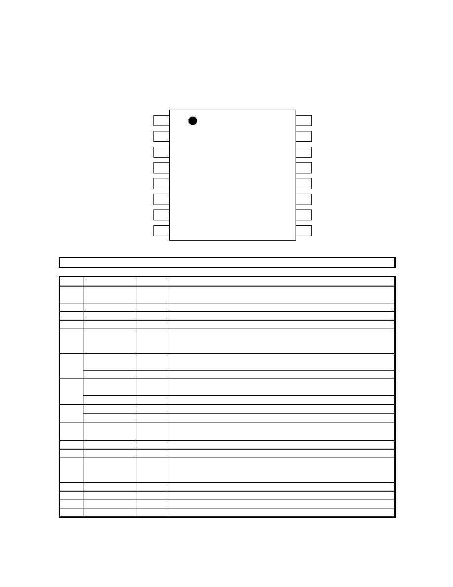
LRCK
BICK
SDTI
Audio
Data
Interface
MCLK
PDN
Modulator
AOUTL
8X
Interpolator
SCF
LPF
AOUTR
VDD
VSS
VCOM
De-emphasis
Control
P/S
µP
Interface
Clock
Divider
SMUTE/CSN
ACKS/CCLK
DIF0/CDTI
Modulator
8X
Interpolator
DZFR
DZFL
SCF
LPF
ATT
ATT
106dB 192kHz 24-Bit 2ch
DAC
AK4384
ASAHI KASEI
[AK4384]
MS0176-E-00
2002/09
- 2 -
n
Ordering Guide
AK4384VT -40
+85
∞
C 16pin TSSOP (0.65mm pitch)
AKD4384 Evaluation Board for AK4384
n
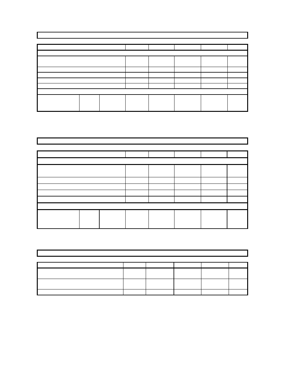
Pin Layout
1
MCLK
LRCK
BICK
SMUTE/CSN
ACKS/CCLK
DIF0/CDTI
Top
View
2
3
4
5
6
7
8
DZFL
DZFR
VSS
VDD
VCOM
AOUTL
AOUTR
P/S
16
15
14
13
12
11
10
9
PDN
SDTI
PIN/FUNCTION
No.
Pin Name
I/O
Function
1
MCLK
I
Master Clock Input Pin
An external TTL clock should be input on this pin.
2
BICK
I
Audio Serial Data Clock Pin
3
SDTI
I
Audio Serial Data Input Pin
4
LRCK
I
L/R Clock Pin
5
PDN
I
Power-Down Mode Pin
When at "L", the AK4384 is in the power-down mode and is held in reset. The
AK4384 should always be reset upon power-up.
SMUTE
I
Soft Mute Pin in parallel mode
"H": Enable, "L": Disable
6
CSN
I
Chip Select Pin in serial mode
ACKS
I
Auto Setting Mode Pin in parallel mode
"L": Manual Setting Mode, "H": Auto Setting Mode
7
CCLK
I
Control Data Clock Pin in serial mode
DIF0
I
Audio Data Interface Format Pin in parallel mode
8
CDTI
I
Control Data Input Pin in serial mode
9
P/S
I
Parallel/Serial Select Pin (Internal pull-up pin)
"L": Serial control mode, "H": Parallel control mode
10
AOUTR
O
Rch Analog Output Pin
11
AOUTL
O
Lch Analog Output Pin
12
VCOM
O
Common Voltage Pin, VDD/2
Normally connected to VSS with a 0.1
µ
F ceramic capacitor in parallel with a
10
µ
F electrolytic cap.
13
VSS
-
Ground Pin
14
VDD
-
Power Supply Pin
15
DZFR
O
Rch Data Zero Input Detect Pin
16
DZFL
O
Lch Data Zero Input Detect Pin
Note: All input pins except pull-up pin should not be left floating.

ASAHI KASEI
[AK4384]
MS0176-E-00
2002/09
- 3 -
ABSOLUTE MAXIMUM RATINGS
(VSS=0V; Note 1)
Parameter
Symbol
min
max
Units
Power Supply
VDD
-0.3
6.0
V
Input Current (any pins except for supplies)
IIN
-
±
10
mA
Input Voltage
VIND
-0.3
VDD+0.3
V
Ambient Operating Temperature
Ta
-40
85
∞
C
Storage Temperature
Tstg
-65
150
∞
C
Note: 1. All voltages with respect to ground.
WARNING: Operation at or beyond these limits may results in permanent damage to the device.
Normal operation is not guaranteed at these extremes.
RECOMMENDED OPERATING CONDITIONS
(VSS=0V; Note 1)
Parameter
Symbol
min
typ
max
Units
Power Supply
VDD
4.5
5.0
5.5
V
*AKM assumes no responsibility for the usage beyond the conditions in this datasheet.

ASAHI KASEI
[AK4384]
MS0176-E-00
2002/09
- 4 -
ANALOG CHARACTERISTICS
(Ta=25
∞
C; VDD=5.0V; fs=44.1kHz; BICK=64fs; Signal Frequency=1kHz; 24bit Input Data;
Measurement frequency=20Hz
20kHz; R
L
5k
; unless otherwise specified)
Parameter
min
typ
max
Units
Resolution
24
Bits
Dynamic Characteristics
(Note 3)
fs=44.1kHz
BW=20kHz
0dBFS
-60dBFS
-94
-42
-84
-
dB
dB
fs=96kHz
BW=40kHz
0dBFS
-60dBFS
-92
-39
-
-
dB
dB
THD+N
fs=192kHz
BW=40kHz
0dBFS
-60dBFS
-92
-39
-
-
dB
dB
Dynamic Range (-60dBFS with A-weighted) (Note 4)
100
106
dB
S/N (A-weighted) (Note 5)
100
106
dB
Interchannel Isolation (1kHz)
90
100
dB
Interchannel Gain Mismatch
0.2
0.5
dB
DC Accuracy
Gain Drift
100
-
ppm/
∞
C
Output Voltage (Note 6)
3.15
3.40
3.65
Vpp
Load Resistance (Note 7)
5
k
Power Supplies
Power Supply Current (VDD)
Normal Operation (PDN = "H", fs
96kHz)
Normal Operation (PDN = "H", fs=192kHz)
Power-Down Mode (PDN = "L") (Note 8)
17
20
10
27
32
100
mA
mA
µA
Notes: 3. Measured by Audio Precision (System Two). Refer to the evaluation board manual.
4. 100dB at 16bit data.
5. S/N does not depend on input bit length.
6. Full-scale voltage (0dB). Output voltage scales with the voltage of VREF,
AOUT (typ.@0dB) = 3.4Vpp ◊ VDD/5.
7. For AC-load.
8. All digital inputs including clock pins (MCLK, BICK and LRCK) are held VDD or VSS.
ASAHI KASEI
[AK4384]
MS0176-E-00
2002/09
- 5 -
SHARP ROLL-OFF FILTER CHARACTERISTICS
(Ta = 25
∞
C; VDD = 4.5
5.5V; fs = 44.1kHz; DEM = OFF; SLOW = "0")
Parameter
Symbol
min
typ
max
Units
Digital filter
Passband
±
0.05dB (Note 9)
-6.0dB
PB
0
-
22.05
20.0
-
kHz
kHz
Stopband (Note 9)
SB
24.1
kHz
Passband Ripple
PR
±
0.02
dB
Stopband Attenuation
SA
54
dB
Group Delay (Note 10)
GD
-
19.3
-
1/fs
Digital Filter + LPF
Frequency Response
20.0kHz
40.0kHz
80.0kHz
fs=44.1kHz
fs=96kHz
fs=192kHz
FR
FR
FR
-
-
-
±
0.03
±
0.03
±
0.03
-
-
-
dB
dB
dB
Notes: 9. The passband and stopband frequencies scale with fs(system sampling rate).
For example, PB=0.4535◊fs (@
±
0.05dB), SB=0.546◊fs.
10. The calculating delay time which occurred by digital filtering. This time is from setting the 16/24bit data
of both channels to input register to the output of analog signal.
SLOW ROLL-OFF FILTER CHARACTERISTICS
(Ta = 25
∞
C; VDD = 4.5 ~ 5.5V; fs = 44.1kHz; DEM = OFF; SLOW = "1")
Parameter
Symbol
min
typ
max
Units
Digital Filter
Passband
±
0.04dB (Note 11)
-3.0dB
PB
0
-
18.2
8.1
-
kHz
kHz
Stopband (Note 11)
SB
39.2
kHz
Passband Ripple
PR
±
0.005
dB
Stopband Attenuation
SA
72
dB
Group Delay (Note 10)
GD
-
19.3
-
1/fs
Digital Filter + LPF
Frequency Response
20.0kHz
40.0kHz
80.0kHz
fs=44.kHz
fs=96kHz
fs=192kHz
FR
FR
FR
-
-
-
+0.02/-5
+0.02/-4
+0.02/-5
-
-
-
dB
dB
dB
Note: 11. The passband and stopband frequencies scale with fs.
For example, PB = 0.185◊fs (@
±
0.04dB), SB = 0.888◊fs.
DC CHARACTERISTICS
(Ta=25
∞
C; VDD=4.5
5.5V)
Parameter
Symbol
min
typ
max
Units
High-Level Input Voltage
Low-Level Input Voltage
VIH
VIL
2.2
-
-
-
-
0.8
V
V
High-Level Output Voltage (Iout=-80µA)
Low-Level Output Voltage (Iout=80µA)
VOH
VOL
VDD-0.4
-
-
-
0.4
V
V
Input Leakage Current (Note 12)
Iin
-
-
±
10
µA
Note: 12. P/S pin has internal pull-up device, normally 100k
.