e
EPAD
TM
Æ
N A
B L
E D
E
A
DVANCED
L
INEAR
D
EVICES,
I
NC.
ORDERING INFORMATION
*N/C pins are internally connected.
Connect to V- to reduce noise
PC, SC PACKAGES
PA, SA PACKAGES
PIN CONFIGURATION
QUAD/DUAL N-CHANNEL ENHANCEMENT MODE EPADÆ
MATCHED PAIR MOSFET ARRAY
V
GS(th)
= +0.8V
ALD110808/ALD110808A/ALD110908/ALD110908A
GENERAL DESCRIPTION
ALD110808A/ALD110808/ALD110908A/ALD110908 are monolithic quad/
dual N-Channel MOSFETs matched at the factory using ALD's proven
EPADÆ CMOS technology. These devices are intended for low voltage,
small signal applications.
These MOSFET devices are built on the same monolithic chip, so they
exhibit excellent temperature tracking characteristics. They are versatile
as circuit elements and are useful design component for a broad range of
analog applications. They are basic building blocks for current sources,
differential amplifier input stages, transmission gates, and multiplexer
applications. For most applications, connect V- and N/C pins to the most
negative voltage potential in the system and V+ pin to the most positive
voltage potential (or left open unused). All other pins must have voltages
within these voltage limits.
ALD110808/ALD110908 devices are built for minimum offset voltage and
differential thermal response, and they are suited for switching and ampli-
fying applications in +1.0V to +10V (+/- 5 V) systems where low input bias
current, low input capacitance and fast switching speed are desired. As
these are MOSFET devices, they feature very large (almost infinite) cur-
rent gain in a low frequency, or near DC, operating environment.
These devices are suitable for use in precision applications which require
very high current gain, beta, such as current mirrors and current sources.
The high input impedance and the high DC current gain of the Field Effect
Transistors result from extremely low current loss through the control gate.
The DC current gain is limited by the gate input leakage current, which is
specified at 30pA at room temperature. For example, DC beta of the
device at a drain current of 3mA and input leakage current of 30pA at
25
∞
C is = 3mA/30pA = 100,000,000.
FEATURES
∑ Enhancement-mode (normally off)
∑ Standard Gate Threshold Voltages: +0.8V
∑ Matched MOSFET to MOSFET characteristics
∑ Tight lot to lot parametric control
∑ Low input capacitance
∑ V
GS(th)
match to 2mV and 10mV
∑ High input impedance -- 10
12
typical
∑ Positive,zero, and negative V
GS(th)
temperature coefficient
∑ DC current gain >10
8
∑ Low input and output leakage currents
Operating Temperature Range*
0
∞
C to +70
∞
C
0
∞
C to +70
∞
C
16-Pin
16-Pin
8-Pin
8Pin
Plastic Dip
SOIC
Plastic Dip
SOIC
Package
Package Package
Package
ALD110808APC ALD110808ASC ALD110908APA ALD110908ASA
ALD110808 PC ALD110808SC ALD110908PA ALD110908SA
APPLICATIONS
∑ Precision current mirrors
∑ Precision current sources
∑ Voltage choppers
∑ Differential amplifier input stage
∑ Voltage comparator
∑ Voltage bias circuits
∑ Sample and Hold
∑ Analog inverter
∑ Level shifters
∑ Source followers and buffers
∑ Current multipliers
∑ Analog switches / multiplexers
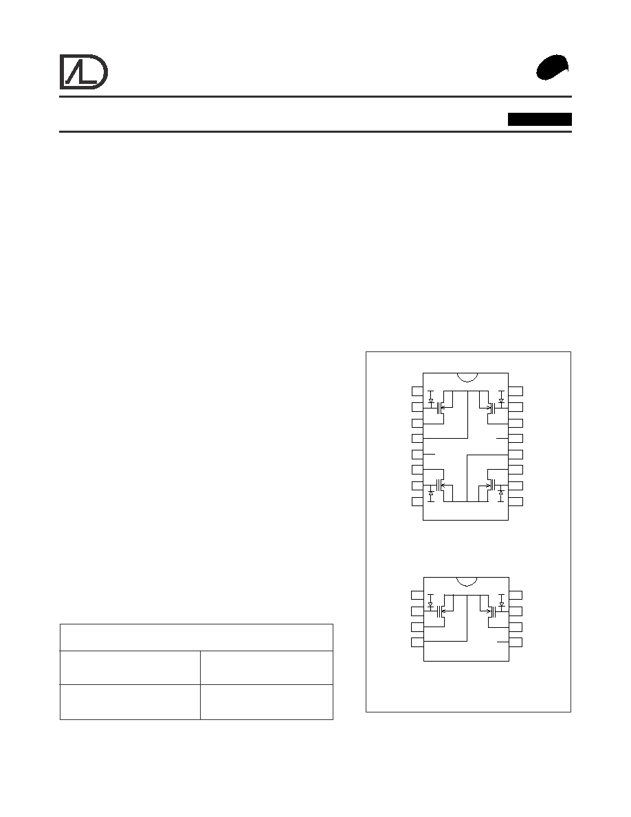
N/C*
1
2
3
14
15
16
4
13
5
12
N/C*
6
7
8
10
11
G
N1
D
N1
N/C*
D
N4
N/C*
G
N4
9
G
N3
D
N3
D
N2
G
N2
V
+
S
34
S
12
V
-
V
+
V
-
ALD110808
M 4
M 3
M 1
M 2
V
-
V
-
V
-
V
-
V-
G
N1
D
N1
N/C*
S
12
D
N2
G
N2
ALD110908
1
2
3
6
7
8
4
5
M 1
M 2
V-
N/C*
V-
V-
Rev 1.0-0506 ©2 005 Advanced Linear Devices, Inc. 415 Tasman Drive, Sunnyvale, California 94089-1706 Tel: (408) 747-1155 Fax: (408) 747-1286
www.aldinc.com
* Contact factory for industrial or military temp. ranges or user-specified threshold voltage values.

ALD110808/ALD110808A/ALD110908/ALD110908A
Advanced Linear Devices
2
Notes:
1
Consists of junction leakage currents
ABSOLUTE MAXIMUM RATINGS
Drain-Source voltage,
V
DS
10.6V
Gate-Source voltage,
V
GS
10.6V
Power dissipation
500 mW
Operating temperature range PA, SA, PC, SC package
0
∞
C to +70
∞
C
Storage temperature range
-65
∞
C to +150
∞
C
Lead temperature, 10 seconds
+260
∞
C
OPERATING ELECTRICAL CHARACTERISTICS
V+ = +5V (or open) V- = GND TA = 25
∞
C unless otherwise specified
CAUTION:
ESD Sensitive Device. Use static control procedures in ESD controlled environment.
ALD110808A / ALD110908A ALD110808/ ALD110908
Parameter
Symbol
Min
Typ
Max
Min
Typ
Max
Unit
Test Condition
Gate Threshold Voltage
VGS(th)
0.78
0.80
0.82
0.78
0.80
0.82
V
IDS =1
µ
A
VDS = 0.1V
Offset Voltage
VOS
1
2
3
10
mV
IDS=1
µ
A
VGS1-VGS2
VGS1-VGS2 Tempco
VOS
5
5
µ
V/
∞
C
VDS1= VDS2
-1.7
-1.7
ID= 1
µ
A
GateThreshold Tempco
VGS(th)
0.0
0.0
mV/
∞
C
ID= 20
µ
A VDS = 0.1V
+1.6
+1.6
ID= 40
µ
A
On Drain Current
IDS (ON)
12.0
12.0
mA
VGS= +10.3V
3.0
3.0
VGS= +4.8V
VDS= +5V
Forward Transconductance
GFS
1.4
1.4
mmho
VGS = +4.8V
VDS = +9.8V
Transconductance Mismatch
GFS
1.8
1.8
%
Output Conductance
GOS
68
68
µ
mho
VGS =+4.8V
VDS = +9.8V
Drain Source On Resistance
RDS (ON)
500
500
VDS = 0.1V
VGS = +4.8V
Drain Source On Resistance
RDS (ON)
0.5
0.5
%
Mismatch
Drain Source Breakdown
BVDSX
10
10
V
IDS = 1.0
µ
A
Voltage
VGS = -0.2V
Drain Source Leakage Current
1
IDS (OFF)
10
100
10
100
pA
VGS = -0.2V
4
4
nA
VDS =10V, TA = 125
∞
C
Gate Leakage Current1
IGSS
3
30
3
30
pA
VDS = 0V VGS = 10V
1
1
nA
TA =125
∞
C
Input Capacitance
CISS
2.5
2.5
pF
Transfer Reverse Capacitance
CRSS
0.1
0.1
pF
Turn-on Delay Time
ton
10
10
ns
V+ = 5V RL= 5K
Turn-off Delay Time
toff
10
10
ns
V+ = 5V RL= 5K
Crosstalk
60
60
dB
f = 100KHz