GENERAL DESCRIPTION
The ALD1106/ALD1116 are
monolithic quad/dual N-channel enhance-
ment mode matched MOSFET transistor arrays intended for a broad range
of precision analog applications. The ALD1106/ALD1116 offer high input
impedance and negative current temperature coefficient. The transistor
pairs are matched for minimum offset voltage and differential thermal
response, and they are designed for switching and amplifying applications
in +2V to +12V systems where low input bias current, low input capacitance
and fast switching speed are desired. These MOSFET devices feature very
large (almost infinite) current gain in a low frequency, or near DC, operating
environment. The ALD1106/ALD1116 are building blocks for differential
amplifier input stages, transmission gates, and multiplexer applications,
current sources and many precision analog circuits.
A
DVANCED
L
INEAR
D
EVICES,
I
NC.
QUAD/DUAL N-CHANNEL MATCHED MOSFET ARRAY
ALD1106/ALD1116
APPLICATIONS
∑ Precision current mirrors
∑ Precision current sources
∑ Voltage choppers
∑ Differential amplifier input stage
∑ Voltage comparator
∑ Data converters
∑ Sample and Hold
∑ Analog signal processing
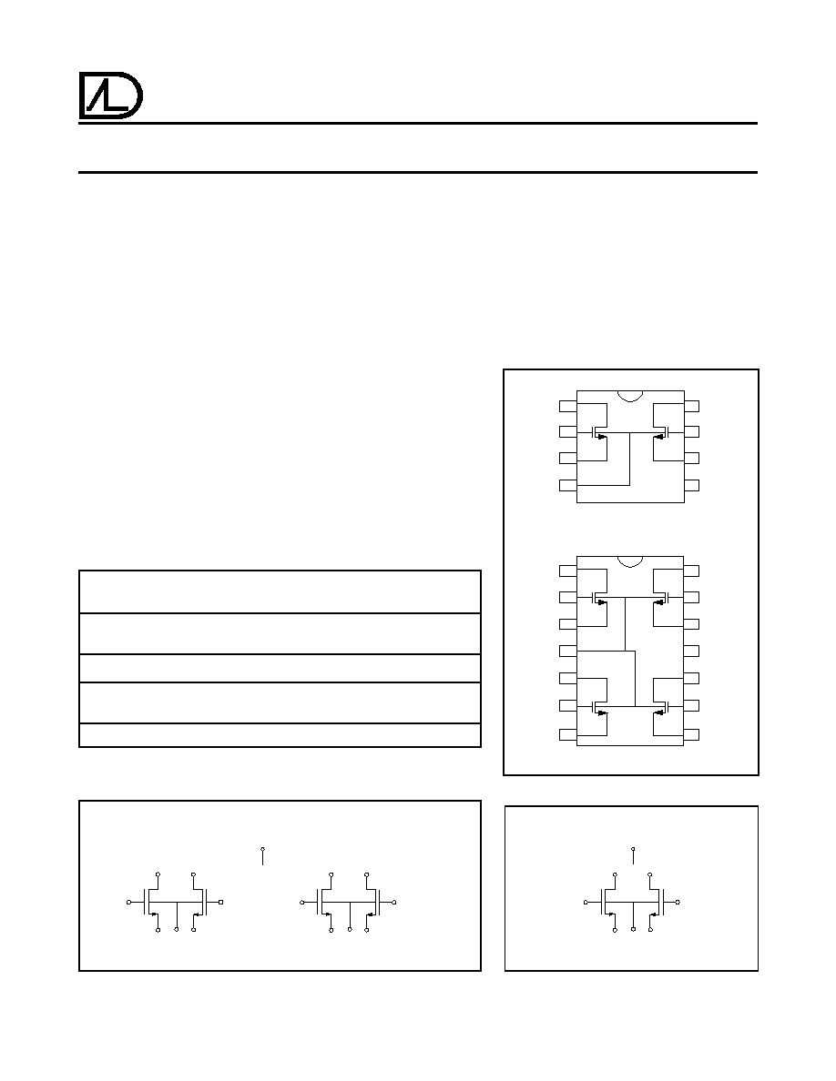
BLOCK DIAGRAM
FEATURES
∑ Low threshold voltage of 0.7V
∑ Low input capacitance
∑ Low Vos 2mV typical
∑ High input impedance -- 10
14
typical
∑ Negative current (I
DS
) temperature coefficient
∑ Enhancement-mode (normally off)
∑ DC current gain 10
9
∑ Low input and output leakage currents
PIN CONFIGURATION
DN2
GN2
SN2
GN1
SN1
1
2
3
4
DA, PA, SA PACKAGE
5
6
7
8
DN1
V+
V-
ALD1116
D
N1
(1)
D
N2
(8)
~
G
N1
(2)
S
N1
(3)
S
N2
(6)
V+ (5)
V- (4)
G
N2
(7)
ALD1116
Operating Temperature Range*
-55
∞
C to +125
∞
C
0
∞
C to +70
∞
C
0
∞
C to +70
∞
C
8-Pin CERDIP
8-Pin Plastic Dip
8-Pin SOIC
Package
Package
Package
ALD1116 DA
ALD1116 PA
ALD1116 SA
14-Pin CERDIP
14-Pin Plastic Dip
14-Pin SOIC
Package
Package
Package
ALD1106 DB
ALD1106 PB
ALD1106 SB
ORDERING INFORMATION
* Contact factory for industrial temperature range.
BLOCK DIAGRAM
D
N1
(1)
D
N2
(14)
G
N1
(2)
S
N1
(3)
S
N2
(12)
V- (4)
G
N2
(13)
D
N3
(10)
D
N4
(5)
G
N3
(9)
S
N3
(8)
S
N4
(7)
~
V+ (11)
V- (4)
G
N4
(6)
ALD1106
DN2
GN2
SN2
GN3
SN3
GN1
SN1
DN4
GN4
1
2
3
4
DB, PB, SB PACKAGE
5
6
7
8
9
10
11
12
13
14
DN1
V
+
V
-
DN3
SN4
1
ALD1106
© 1998 Advanced Linear Devices, Inc. 415 Tasman Drive, Sunnyvale, California 94089 -1706 Tel: (408) 747-1155 Fax: (408) 747-1286 http://www.aldinc.com

ALD1106/ALD1116
Advanced Linear Devices
2
ABSOLUTE MAXIMUM RATINGS
Drain-source voltage, V
DS
13.2V
Gate-source voltage, V
GS
13.2V
Power dissipation
500 mW
Operating temperature range
PA, SA, PB, SB package
0
∞
C to +70
∞
C
DA, DB package
-55
∞
C to +125
∞
C
Storage temperature range
-65
∞
C to +150
∞
C
Lead temperature, 10 seconds
+260
∞
C
Gate Threshold
V
T
0.4
0.7
1.0
0.4
0.7
1.0
V
I
DS
= 1.0
µ
A V
GS
= V
DS
Voltage
Offset Voltage
V
OS
2
10
2
10
mV
I
DS
= 10
µ
A V
GS
= V
DS
V
GS1
-V
GS2
Gate Threshold
Temperature
TC
VT
-1.2
-1.2
mV/
∞
C
Drift
2
On Drain
I
DS (ON)
3.0
4.8
3.0
4.8
mA
V
GS
= V
DS
= 5V
Current
Transconductance
G
IS
1.0
1.8
1.0
1.8
mmho V
DS
= 5V I
DS
= 10mA
Mismatch
G
fs
0.5
0.5
%
Output
G
OS
200
200
µ
mho
V
DS
= 5V I
DS
= 10mA
Conductance
Drain Source R
DS (ON)
350
500
350
500
V
DS
= 0.1V V
GS
= 5V
On Resistance
Drain Source
On Resistence
DS (ON)
0.5
0.5
%
V
DS
= 0.1V V
GS
= 5V
Mismatch
Drain Source
Breakdown
BV
DSS
12
12
V
I
DS
= 1.0
µ
A V
GS
= 0V
Voltage
Off Drain
I
DS (OFF)
10
400
10
400
pA
V
DS
=12V V
GS
= 0V
Current
1
4
4
nA
T
A
= 125
∞
C
Gate Leakage
I
GSS
0.1
10
0.1
10
pA
V
DS
= 0V V
GS
= 12V
Current
1
1
nA
T
A
= 125
∞
C
Input
C
ISS
1
3
1
3
pF
Capacitance
2
OPERATING ELECTRICAL CHARACTERISTICS
T
A
= 25
∞
C unless otherwise specified
ALD1106
ALD1116
Test
Parameter
Symbol
Min
Typ
Max
Min
Typ
Max
Unit
Conditions
Notes:
1
Consists of junction leakage currents
2
Sample tested parameters
ALD1106/ALD1116
Advanced Linear Devices
3
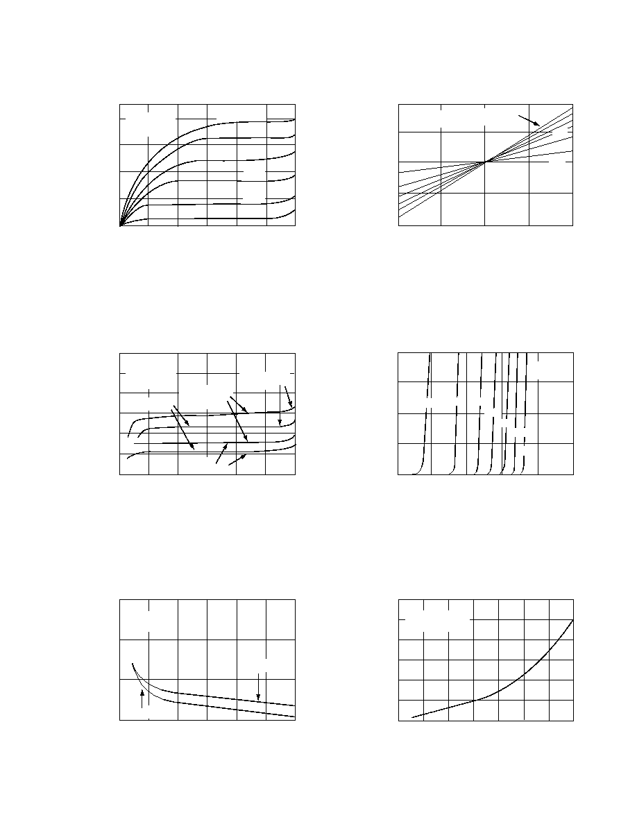
TYPICAL PERFORMANCE CHARACTERISITCS
OUTPUT CHARACTERISTICS
DRAIN SOURCE CURRENT
(mA)
20
15
10
0
5
V
BS
= 0V
T
A
= 25
∞
C
V
GS
= 12V
10V
8V
6V
4V
2V
DRAIN SOURCE VOLTAGE (V)
0
2
4
6
8
10
12
LOW VOLTAGE OUTPUT
CHARACTERISTICS
DRAIN SOURCE VOLTAGE (mV)
DRAIN SOURCE CURRENT
(
µ
A)
-160
-80
0
80
160
-1000
1000
500
0
-500
4V
V
GS
= 12V
6V
V
BS
= 0V
T
A
= 25
∞
C
2V
GATE SOURCE VOLTAGE (V)
TRANSFER CHARACTERISTIC
WITH SUBSTRATE BIAS
DRAIN SOURCE CURRENT
(
µ
A)
20
15
10
5
0
0
0.8
1.6
2.4
3.2
4.0
V
BS
= 0V
-2V
-4V
-6V
-8V
-10V
-12V
V
GS
= V
DS
T
A
= 25
∞
C
GATE SOURCE VOLTAGE (V)
DRAIN SOURCE ON RESISTANCE
R
DS (ON)
vs. GATE SOURCE VOLTAGE
DRAIN SOURCE ON RESISTANCE
(K
)
100
10
1
0.1
2
0
4
6
8
10
12
V
DS
= 0.2V
V
BS
= 0V
T
A
= +25
∞
C
T
A
= +125
∞
C
OFF DRAIN CURRENT vs.
AMBIENT TEMPERATURE
AMBIENT TEMPERATURE (
∞
C)
OFF DRAIN SOURCE CURRENT
(pA)
-50
-25
+25
+50
+75
+125
+100
0
V
DS
= +12V
V
GS
= V
BS
= 0V
1
10
100
1000
FORWARD TRANSCONDUCTANCE
(mmho)
FORWARD TRANSCONDUCTANCE
vs. DRAIN SOURCE VOLTAGE
DRAIN SOURCE VOLTAGE (V)
20
10
2
1
0.5
5
0.2
0
2
4
6
8
10
12
I
DS
= 1mA
T
A
= +25
∞
C
I
DS
= 10mA
T
A
= +125
∞
C
V
BS
= 0V
f = 1KHz
