FEATURES
∑
Electrically Programmable Analog Device
CMOS Technology
∑
Operates from 2V, 3V, 5V to 10V
∑
Flexible basic circuit building block and design element
∑
Very high resolution -- average e-trim voltage
resolution of 0.1mV
∑
Wide dynamic range -- current levels from 0.1
µ
A
to 3000
µ
A
∑
Voltage adjustment range from 1.000V to 3.000V
in 0.1mV steps
∑
Proven, non-volatile CMOS technology
∑
Typical 10 years drift of less than 2mV
∑
Usable in voltage mode or current mode
∑
High input impedance -- 10
12
∑
Very high DC current gain -- greater than 10
9
∑
Device operating current has positive temperature
coefficient range and negative temperature
coefficient range with cross-over zero temperature
coefficient current level at 68
µ
A
∑
Tight matching and tracking of on-resistance
between different devices with e-trim
∑
Wide dynamic resistance matching range
∑
Very low input currents and leakage currents
∑
Low cost, monolithic technology
∑
Application-specific or in-system programming modes
∑
Optional user software-controlled automation
∑
Optional e-trim of any standard/custom configuration
∑
Micropower operation
∑
Available in standard PDIP, SOIC and hermetic CDIP packages
∑
Suitable for matched-pair balanced circuit configuration
∑
Suitable for both coarse and fine trimming as well as matched
MOSFET array applications
QUAD/DUAL EPAD
Æ
PRECISION MATCHED PAIR N-CHANNEL MOSFET ARRAY
A
DVANCED
L
INEAR
D
EVICES,
I
NC.
ALD1123E/ALD1121E
BENEFITS
∑
Precision matched electrically after packaging
∑
Simple, elegant single-chip user option
to trimming voltage/current values
∑
Excellent device matching characteristics with
or without additional electrical trim
∑
Remotely and electrically trim parameters on
circuits that are physically inaccessible
∑
Usable in environmentally sealed circuits
∑
No mechanical moving parts -- high G-shock
tolerance
∑
Improved reliability, dependability, dust and
moisture resistance
∑
Cost and labor savings
∑
Small footprint for high board density
applications
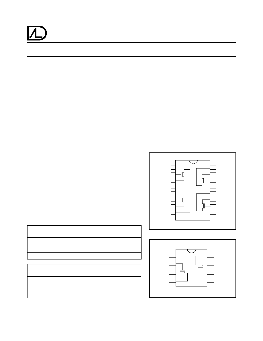
PIN CONFIGURATION
PIN CONFIGURATION
Operating Temperature Range*
0
∞
C to +70
∞
C
0
∞
C to +70
∞
C
8-Pin
8-Pin
Plastic Dip
SOIC
Package
Package
ALD1121E PA
ALD1121E SA
Operating Temperature Range*
0
∞
C to +70
∞
C
0
∞
C to +70
∞
C
16-Pin
16-Pin
Plastic Dip
SOIC
Package
Package
ALD1123E PC
ALD1123E SC
ORDERING INFORMATION
* Contact factory for industrial temperature range
© 2003 Advanced Linear Devices, Inc. 415 Tasman Drive, Sunnyvale, California 94089 -1706 Tel: (408) 747-1155 Fax: (408) 747-1286 www.aldinc.com
1
2
3
6
7
8
4
5
G
N1
D
N1
S
N2
D
N2
DA, PA, SA PACKAGE
ALD1121E
S
N1,
V-
G
N2
P
N2
P
N1
M 1
M 2
S
N2
1
2
3
14
15
16
4
13
5
12
P
N3
6
7
8
10
11
G
N1
D
N1
P
N1
G
N4
V-
2,
S
N4
D
N4
9
G
N3
D
N3
G
N2
D
N2
DC, PC, SC PACKAGE
P
N2
S
N3
V-
1,
S
N1
P
N4
ALD1123E
M 1
M 2
M 4
M 3

ALD1123E/ALD1121E
Advanced Linear Devices
2
GENERAL DESCRIPTION
ALD1123E/ALD1121E are monolithic quad/dual EPADÆ (Electrically Program-
mable Analog Device) N-channel MOSFETs with electrically adjustable threshold
(turn-on) voltage. The ALD1123E/ALD1121E are precision matched and adjusted
(e-trimmed) at the factory resulting in quad/dual MOSFETs that are highly matched
in electrical characteristics. The ALD1123E has four (4) separate source pins. SN1,
SN2 share a common substrate pin V-1 which has to be connected to the most
negative voltage potential. Likewise, SN3, SN4 share a common substrate pin V-2
which has to be connected to the negative voltage potential for SN3, SN4. The
ALD1121E has two (2) separate source pins (SN1, SN2). Both SN1, SN2 share a
common substrate pin 4 which has to be connected to the most negative voltage
potential.
Using an ALD1123E/ALD1121E MOSFET array is simple and straight forward. The
MOSFETs function in electrical characteristics as n-channel MOSFETs except that
all the devices have exceptional matching to each other. For a given input voltage,
the threshold voltage of a MOSFET device determines its drain on-current, resulting
in an on-resistance characteristic that can be precisely preset and then controlled
by the input voltage very accurately. Since these devices are on the same monolithic
chip, they also exhibit excellent tempco matching characteristics.
These MOSFET devices have very low input currents, and as a result a very high
input impedance (>10 12 Ohm). The gate voltage from a control source can drive
many MOSFET inputs with practically no loading effects. Used in precision current
mirror or current multiplier applications, they can be used to provide a current source
over a 100 nA to 3 mA range, and with either a positive, negative or zero tempco.
Optional EPAD Threshold Voltage Trimming By User
The basic EPAD MOSFET device is a monotonically adjustable device which means
the device can normally be e-trimmed to increase in threshold voltage and to
decrease in drain-on current as a function of a given input bias voltage. Used as an
in-circuit element for trimming or setting a combination of voltage and/or current
characteristics, it can be e-trimmed remotely and automatically. Once e-trimmed,
the set voltage and current levels are stored indefinitely inside the device as a
nonvolatile stored charge, which is not affected during normal operation of the
device, even when power is turned off. A given EPAD device can be adjusted many
times to continually increase its threshold voltage. A pair of EPAD devices can also
be connected differentially such that one device is used to adjust a parameter in one
direction and the other device is used to adjust the same parameter in the other
direction.
The ALD1123E/ALD1121E can be e-trimmed with the ALD EPAD programmer to
obtain the desired voltage and current levels. Or they can be e-trimmed as an active
in-system element in a user system, via user designed interface circuitry. PN1, PN2,
etc., are pins required for optional e-trim of respective MOSFET devices. If unused,
these pins are to be connected to V- or ground. For more information, see
Application Note AN1108.
APPLICATIONS
∑
Precision PC-based electronic calibration
∑
Automated voltage trimming or setting
∑
Remote voltage or current adjustment of
inaccessible nodes
∑
PCMCIA based instrumentation trimming
∑
Electrically adjusted resistive load
∑
Temperature compensated current sources
and current mirrors
∑
Electrically trimmed/calibrated current
sources
∑
Permanent precision preset voltage level
shifter
∑
Low temperature coefficient voltage and/or
current bias circuits
∑
Multiple preset voltage bias circuits
∑
Multiple channel resistor pull-up or pull-down
circuits
∑
Microprocessor based process control systems
∑
Portable data acquisition systems
∑
Battery operated terminals and instruments
∑
Remote telemetry systems
∑
E-trim gain amplifiers
∑
Low level signal conditioning
∑
Sensor and transducer bias currents
∑
Neural networks
BLOCK DIAGRAM
BLOCK DIAGRAM
ALD1121E
ALD1123E
P
N1
(1)
D
N1
(3)
G
N1
(2)
D
N2
(7)
P
N2
(5)
G
N2
(6)
S
N2
(8)
M 1
M 2
S
N1
(4)
V- (4)
~
M 1
M 2
M 3
M 4
P
N4
(5)
P
N1
(1)
D
N1
(3)
G
N1
(2)
D
N2
(15)
P
N2
(13)
G
N2
(14)
P
N3
(9)
D
N3
(11)
G
N3
(10)
D
N4
(7)
G
N4
(6)
S
N1
(4)
S
N2
(16)
S
N3
(12)
S
N4
(8)
V-
2
(8)
~
V-
1
(4)
~
ALD1123E/ALD1121E
Advanced Linear Devices
3
Drain to Source Voltage
1
V
DS
10.0
10.0
V
Initial Threshold Voltage
2
V
t i
0.990
1.000
1.010
0.990
1.000
1.010
V
I
DS
= 1
µ
A T
A
= 21
∞
C
E-trim Vt Range
V
t
1.000
3.000
1.000
3.000
V
Drain - Gate Connected
TCV
DS
-1.6
-1.6
mV/
∞
C
I
D
= 5
µ
A
Voltage Tempco
-0.3
-0.3
mV/
∞
C
I
D
= 50
µ
A
0.0
0.0
mV/
∞
C
I
D
= 68
µ
A
+2.7
+2.7
mV/
∞
C
I
D
= 500
µ
A
Initial Offset Voltage
3
V
OS i
1
5
1
5
mV
Tempco of V
OS
TCV
OS
5
5
µ
V/
∞
C
V
DS1
= V
DS2
Differential Threshold Voltage
4
DV
t
2.000
2.000
V
Tempco of Differential
Threshold Voltage
4
TCDV
t
0.033
0.033
mV/
∞
C
Long Term Drift
V
t
/
t
-0.02
-0.05
-0.02
-0.05
mV
1000 Hours
Long Term Drift Match
V
t
/
t
-5
-5
µ
V
1000 Hours
Drain Source On Current
I
DS(ON)
3.0
3.0
mA
V
G
=V
D
= 5V V
S
= 0V
V
t
= 1.0
Drain Source On Current
4
I
DS(ON)
0.8
0.8
mA
V
G
=V
D =
5V V
S =
0V
V
t
= 3.0
Initial Zero Tempco Voltage
3
V
ZTCi
1.52
1.52
V
V
t
= 1.000V
Zero Tempco Current
I
ZTC
68
68
µ
A
Initial On-Resistance
3
R
ON i
500
500
V
GS
°= 5V V
DS
= 0.1V
On-Resistance Match
R
ON
0.5
0.5
%
ABSOLUTE MAXIMUM RATINGS
Supply voltage, V
+
referenced to V
-
-0.3V to +13.2V
Supply voltage, V
S
referenced to V
-
±
6.6V
Differential input voltage range
0.3V to V
+
+0.3V
Power dissipation
600 mW
Operating temperature range PA, SA, PC, SC package
0
∞
C to +70
∞
C
DA, DC package
-55
∞
C to +125
∞
C
Storage temperature range
-65
∞
C to +150
∞
C
Lead temperature, 10 seconds
+260
∞
C
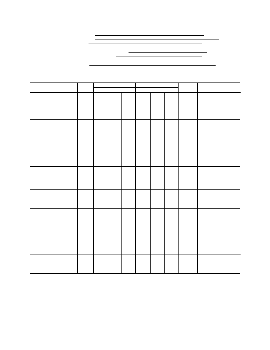
OPERATING ELECTRICAL CHARACTERISTICS
T
A
= 25
∞
C V+ = +5.0V unless otherwise specified
ALD1123E
ALD1121E
Test
Parameter
Symbol
Min
Typ
Max
Min
Typ
Max
Unit
Conditions
NOTES:
1. V+ must be the most positive supply rail and V- must be at the most negative supply rail. Source terminals other than those labeled as V- can be at
any voltage between V- and V+.
2. Initial Threshold Voltage is set at the factory. If no EPAD Vt trimming is intended by user, then this is also the final or permanent threshold voltage
value.
3. Initial and Final values are the same unless deliberately changed by user.
4. These parameters apply only when Vt of one or more of the devices are to be changed by user.
ALD1123E/ALD1121E
Advanced Linear Devices
4
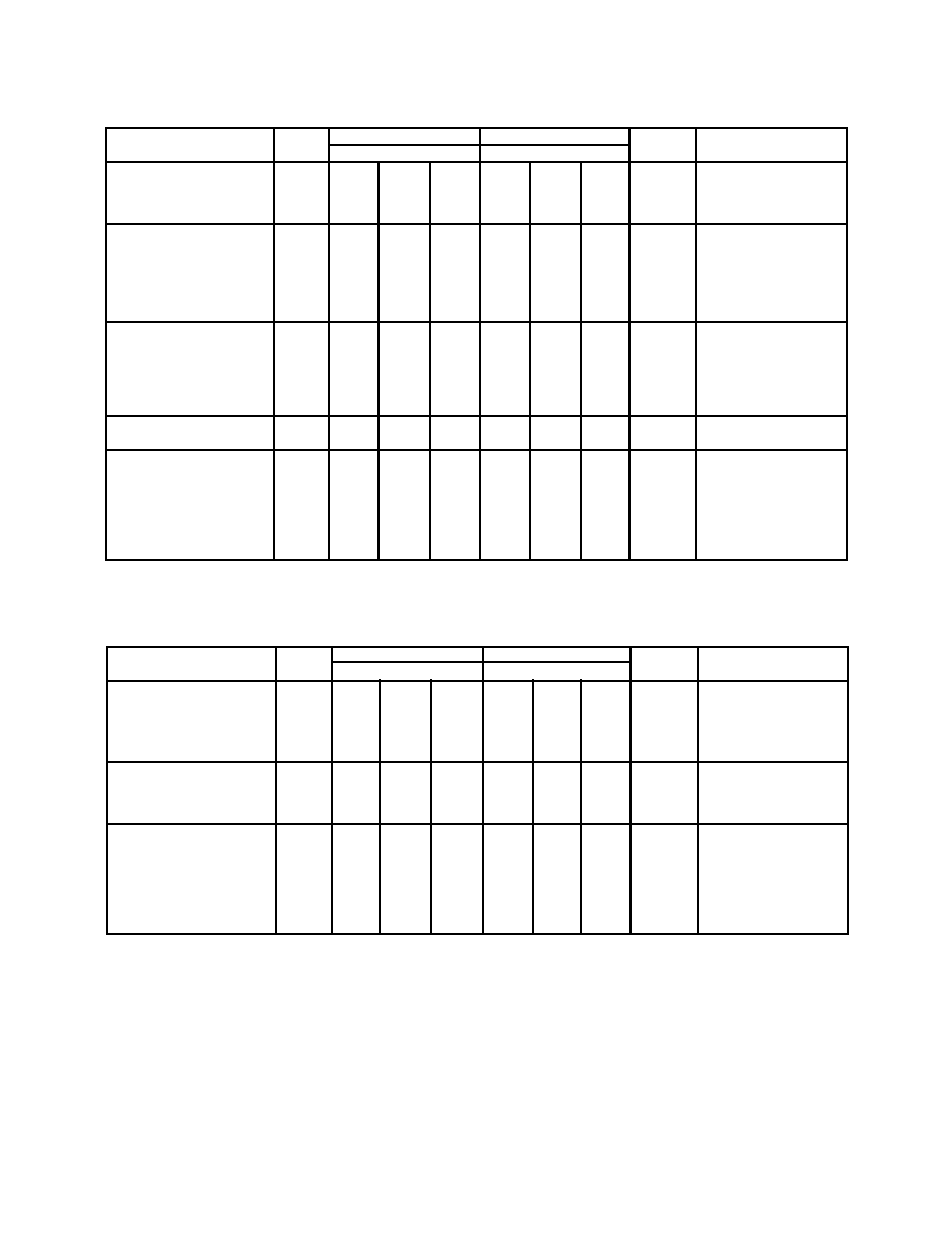
E-TRIM CHARACTERISTICS
T
A
= 25
∞
C V+ = +5.0V unless otherwise specified
ALD1123E
ALD1121E
Test
Parameter
Symbol
Min
Typ
Max
Min
Typ
Max
Unit
Conditions
E-trim V
t
Range
4
V
t
1.000
3.000
1.000
3.000
V
Resolution of V
t
E-trim Pulse Step
4
RV
t
0.1
1
0.1
1
mV
Change in V
t
Per
V
t
/ N
0.5
0.5
mV/ pulse
V
t
= 1.0V
E-trim Pulse
4
0.05
0.05
V
t
= 2.5V
E-trim Pulse Voltage
4
Vp
11.75
12.00
12.25
11.75
12.00
12.25
V
E-trim Pulse Current
4
Ip
2
2
mA
Pulse Frequency
4
pulse
50
50
KH
Z
Transconductance
gm
1.4
1.4
mA/V
V
D
= 10V,V
G
=V
t
+ 4.0
Transconductance Match
gm
25
25
µ
A/V
V
D
= 10V,V
G
=V
t
+ 4.0
Low Level Output
Conductance
g
OL
6
6
µ
A/V
V
G
= V
t
+0.5V
High Level Output
Conductance
g
OH
68
68
µ
A/V
V
G
= V
t
+4.0V
Drain Off Leakage Current
I
D(OFF)
5
400
5
400
pA
4
4
nA
T
A
= 125
∞
C
Gate Leakage Current
I
GSS
10
100
10
100
pA
1
1
nA
T
A
= 125
∞
C
Input Capacitance
C
ISS
25
25
pF
Cross Talk
60
60
dB
f = 100KHz
Relaxation Time Constant
4
t
RLX
2
2
Hours
Relaxation Voltage
4
V
RLX
-0.3
-0.3
%
1.0V
V
t
3.0V
OPERATING ELECTRICAL CHARACTERISTICS (cont'd)
T
A
= 25
∞
C V+ = +5.0V unless otherwise specified
ALD1123E
ALD1121E
Test
Parameter
Symbol
Min
Typ
Max
Min
Typ
Max
Unit
Conditions
ALD1123E/ALD1121E
Advanced Linear Devices
5
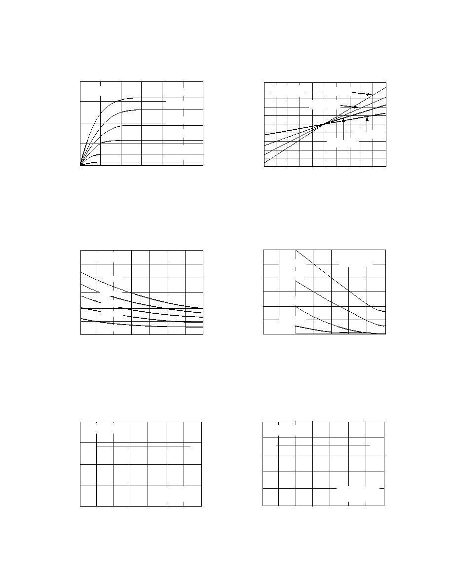
TYPICAL PERFORMANCE CHARACTERISTICS
OUTPUT CHARACTERISTICS
DRAIN SOURCE ON VOLTAGE (V)
0
2
4
6
10
12
8
20
15
10
5
0
DRAIN SOURCE ON CURRENT
(mA)
T
A
= +25
∞
C
V
GS
= +12V
V
GS
= + 2V
V
GS
= + 4V
V
GS
= + 6V
V
GS
= + 8V
V
GS
= +10V
OUTPUT CHARACTERISTICS
-200 -160 -120 -80 -40
+200
+1.0
0
0 40 80 120 160
DRAIN SOURCE VOLTAGE (mV)
DRAIN SOURCE ON CURRENT
(mA)
-1.0
V
GS
= +12V
V
GS
= +6V
V
GS
= +8V
V
GS
= +10V
T
A
= +25
∞
C
TRANSCONDUCTANCE vs.
THRESHOLD VOLTAGE
THRESHOLD VOLTAGE (V)
0
0.5
1.0
1.5
2.0
3.0
3.5
2.5
2.0
1.5
1.0
5.0
TRANSCONDUCTANCE
(
mA/V)
T
A
= +25
∞
C
0
V
GS
= V
t
+ 4.0V
V
DS
= 10V
HIGH LEVEL OUTPUT CONDUCTANCE
vs.THRESHOLD VOLTAGE
THRESHOLD VOLTAGE (V)
0
0.5
1.0
1.5
2.0
3.0
3.5
2.5
75
70
60
50
HIGH LEVEL OUTPUT
CONDUCTANCE (
µ
A/V)
T
A
= +25
∞
C
V
GS
= V
t
+ 4.0V
V
DS
= 5.0V
DRAIN SOURCE ON CURRENT vs.
THRESHOLD VOLTAGE
THRESHOLD VOLTAGE (V)
0
0.5
1.0
1.5
2.0
3.0
3.5
2.5
T
A
= +25
∞
C
V
DS
= +5.0V
DRAIN SOURCE ON CURRENT
(mA)
3.0
2.0
1.0
0
V
GS
= +5V
V
GS
= +1V
V
GS
= +2V
V
GS
= +3V
V
GS
= +4V
DRAIN SOURCE ON CURRENT vs.
AMBIENT TEMPERATURE
6
5
4
3
2
1
0
AMBIENT TEMPERATURE (
∞
C)
-50 -25 0 25 50 75 100 125
DRAIN SOURCE ON CURRENT
(mA)
V
G
= 5V
V
t
= 1.0V
V
t
= 1.5V
V
t
= 3.0V
V
t
= 2.0V
V
t
= 2.5V