Operating Temperature Range *
-55
∞
C to +125
∞
C
0
∞
C to +70
∞
C
0
∞
C to +70
∞
C
14-Pin
14-Pin
14-Pin
CERDIP
Small Outline
Plastic Dip
Package
Package (SOIC)
Package
ALD 4301ADB
ALD4301ASB
ALD4301APB
ALD 4301DB
ALD4301SB
ALD4301PB
QUAD PRECISION CMOS VOLTAGE COMPARATOR WITH OPEN DRAIN DRIVER
ALD4301A/ALD4301
A
DVANCED
L
INEAR
D
EVICES,
I
NC.
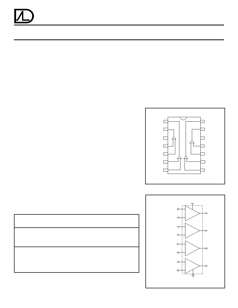
ORDERING INFORMATION
PIN CONFIGURATION
BLOCK DIAGRAM
GENERAL DESCRIPTION
The ALD4301A/ALD4301 is a monolithic high performance quad
voltage comparator built with advanced silicon gate CMOS technol-
ogy. It features very high typical input impedance of 10
12
; low input
bias current of 10pA; fast response time of 300ns; very low power
dissipation of 55
µ
A per comparator; high output drive and single +5V
or dual
±
5V power supply operation.
The input voltage range includes ground, making this comparator ideal
for low level signal detection with high source impedance. The outputs
are open-drain configuration, allowing maximum application flexibility.
The outputs can be connected to a higher external voltage than V
+
and
used in a wired-OR connection with other open drain circuits such as
ALD2301/ALD2303. They can also be used with push-pull output
types such as ALD2302/ALD4302 voltage comparators simultaneously
with open drain comparators using a common V+. The ALD4301A/
ALD4301 is ideal for a great variety of voltage comparator applica-
tions, especially detection circuits requiring very low input currents
and low standby power, yet retaining high output current capability.
FEATURES
∑ Fanout of 30 LS TTL loads
∑ Low supply current of 55
µ
A/comparator typical
∑ Pinout/Functional equivalent to LM393 types
∑ Extremely low input bias currents -- 10pA typical
∑ Virtually eliminates source impedance effects
∑ Low operating supply voltage of 3V to 12V
∑ Single +5V and dual supply
±
5V operation
∑ High speed for both large signal and low level
signals -- 300ns typical for TTL inputs
∑ CMOS, NMOS and TTL compatible
∑ Wired-OR open drain outputs
∑ High output sinking current -- 60mA typical
∑ Low supply current spikes
∑ High gain
APPLICATIONS
∑ High source impedance voltage
comparison circuits
∑ Dual/Quad limit window comparator
∑ Power supply voltage monitor
∑ Photo-detector sensor circuit
∑ Relay or LED driver
∑ Oscillators
∑ Battery operated instruments
∑ Remote signal detection
* Contact factory for industrial temperature range
© 2005 Advanced Linear Devices, Inc. 415 Tasman Drive, Sunnyvale, California 94089 -1706 Tel: (408) 747-1155 Fax: (408) 747-1286 http://www.aldinc.com
DB, PB, SB PACKAGE
+IN
1
-IN
2
+IN
2
03
04
GND
-IN
4
+IN
3
-IN
3
02
01
-IN
1
+IN
4
1
14
V
+
2
3
13
12
11
10
9
8
4
5
6
7
V
+
(3)
INVERTING INPUT
- IN
1
(4)
NONINVERTING INPUT
+ IN
1
(5)
NONINVERTING INPUT
+ IN
2
(7)
INVERTING INPUT
- IN
2
(6)
NONINVERTING INPUT
+ IN
3
(9)
INVERTING INPUT
- IN
3
(8)
INVERTING INPUT
- IN
4
(10)
(12)
NONINVERTING INPUT
+ IN
4
(11)
-
+
-
+
-
+
-
+
(2) OUT
1
(1) OUT
2
(14) OUT
3
(13) OUT
4

ALD4301A/ALD4301
Advanced Linear Devices
ABSOLUTE MAXIMUM RATINGS
Supply voltage, V
+
13.2V
Differential input voltage range
-0.3V to V
+
+0.3V
Power dissipation
600 mW
Operating temperature range
PB, SB package
0
∞
C to +70
∞
C
DB package
-55
∞
C to +125
∞
C
Storage temperature range
-65
∞
C to +150
∞
C
Lead temperature, 10 seconds
+260
∞
C
OPERATING ELECTRICAL CHARACTERISTICS
T
A
= 25
∞
C V+= +5V unless otherwise specified
4301A
4301
Test
Parameter
Symbol
Min
Typ
Max
Min
Typ
Max
Unit
Conditions
Notes:
1
Consists of junction leakage currents
2
Sample tested parameters
Voltage
V
+
3
12
3
12
V
Single supply
Supply
±
1.5
±
6
±
1.5
±
6
V
Dual supplies
Supply
I
S
220
350
220
350
µ
A
No load
Current
Voltage
A
VD
50
150
50
150
V/mV
R
LOAD
15K
Gain
Input Offset
V
OS
5
10
mV
R
LOAD
1.5K
Voltage
Input Offset
I
OS
0.1
30
0.1
30
pA
Current
1
Input Bias
I
B
0.1
30
0.1
30
pA
Current
1
Common
Mode Input
V
ICR
-0.3
V
+-1.5
-0.3
V
+
-1.5
V
Voltage
Range
2
Low Level
I
SINK
=12mA
Output
V
OL
0.15
0.4
0.15
0.4
V
V
INPUT
=1V
Voltage
Differential
Low Level
Output
I
OL
24
60
24
60
mA
V
OL
=1.0V
Current
High Level
Leakage
I
LH
0.1
20
0.1
20
nA
V
OH
= 5.0 V
Current
Response
R
L
=5.1K
Time
2
t
RP
650
650
ns
C
L
= 15pF
100mV Input
Step/5mV
Overdrive
RL = 5.1K
300
300
ns
C
L
= 15pF
TTL- Level Input
Step
ALD4301A/ALD4301
Advanced Linear Devices
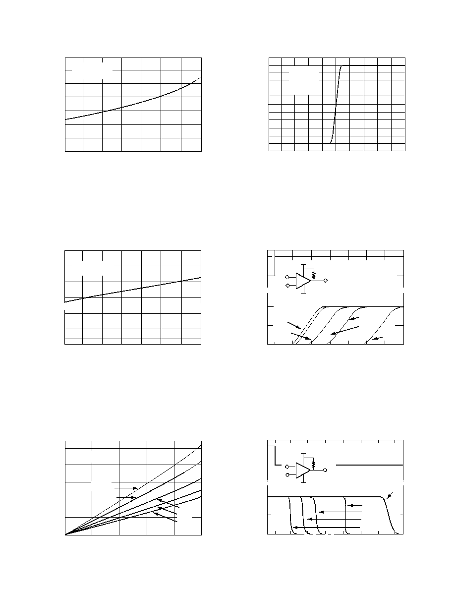
TYPICAL PERFORMANCE CHARACTERISTICS
SATURATION VOLTAGE vs.
SINK CURRENT
OUTPUT SINK CURRENT (mA)
0
15
30
45
60
75
1.5
1.2
0.9
0.6
0.3
0.0
OUTPUT SATURATION
VOLTAGE (V)
V
S
=
±
2.5V
-55
∞
C
25
∞
C
-25
∞
C
85
∞
C
125
∞
C
SATURATION VOLTAGE
vs.TEMPERATURE
TEM PERATURE (
∞
C)
-55
-25
0
25
50
125
100
75
1.4
1.2
1.0
0.8
0.6
0.4
0.2
SATURATION VOLTAGE (V)
0
V
S
=
±
2.5V
I
SINK
= 50mA
TRANSFER FUNCTION
DIFFERENTIAL INPUT VOLTAGE (mV)
+6.0
-6.0
0.0
OUTPUT VOLTAGE (V)
+2.5
0.0
-2.5
TA = 25
∞
C
VS =
±
6V
RL = 5.1K
COMMON - MODE VOLTAGE REFERRED
TO SUPPLY VOLTAGE
TEMPERATURE (
∞
C)
0.5
V+
-0.5
-1.0
0.5
V-
-0.5
COMMON - MODE VOLTAGE LIMITS (V)
-55
-25
0
25
50
125
100
75
V
S
=
±
2.5V
TIM E (
µ
s)
0.0
0.2
0.4
0.8
0.6
1.2
1.0
1.4
RESPONSE TIME FOR VARIOUS
INPUT OVERDRIVES
+2.5
0
100
0.0
-2.5
INPUT
VOLTAGE (mV)
OUTPUT
VOLTAGE (V)
5mV
10mV
20mV
50mV
T
A
= 25
∞
C
V
S
=
±
2.5V
0V
V
IN
V+
V-
V
OUT
+
-
5.1K
2mV
TIM E (
µ
s)
0.0
0.2
0.4
0.8
0.6
1.2
1.0
1.4
RESPONSE TIME FOR VARIOUS
INPUT OVERDRIVES
+2.5
100
0
0.0
-2.5
INPUT
VOLTAGE (mV)
OUTPUT
VOLTAGE (V)
50mV
20mV
5mV
10mV
T
A
= 25
∞
C
V
S
=
±
2.5V
0V
V
IN
V+
V-
V
OUT
+
-
2mV
5.1K
ALD4301A/ALD4301
Advanced Linear Devices
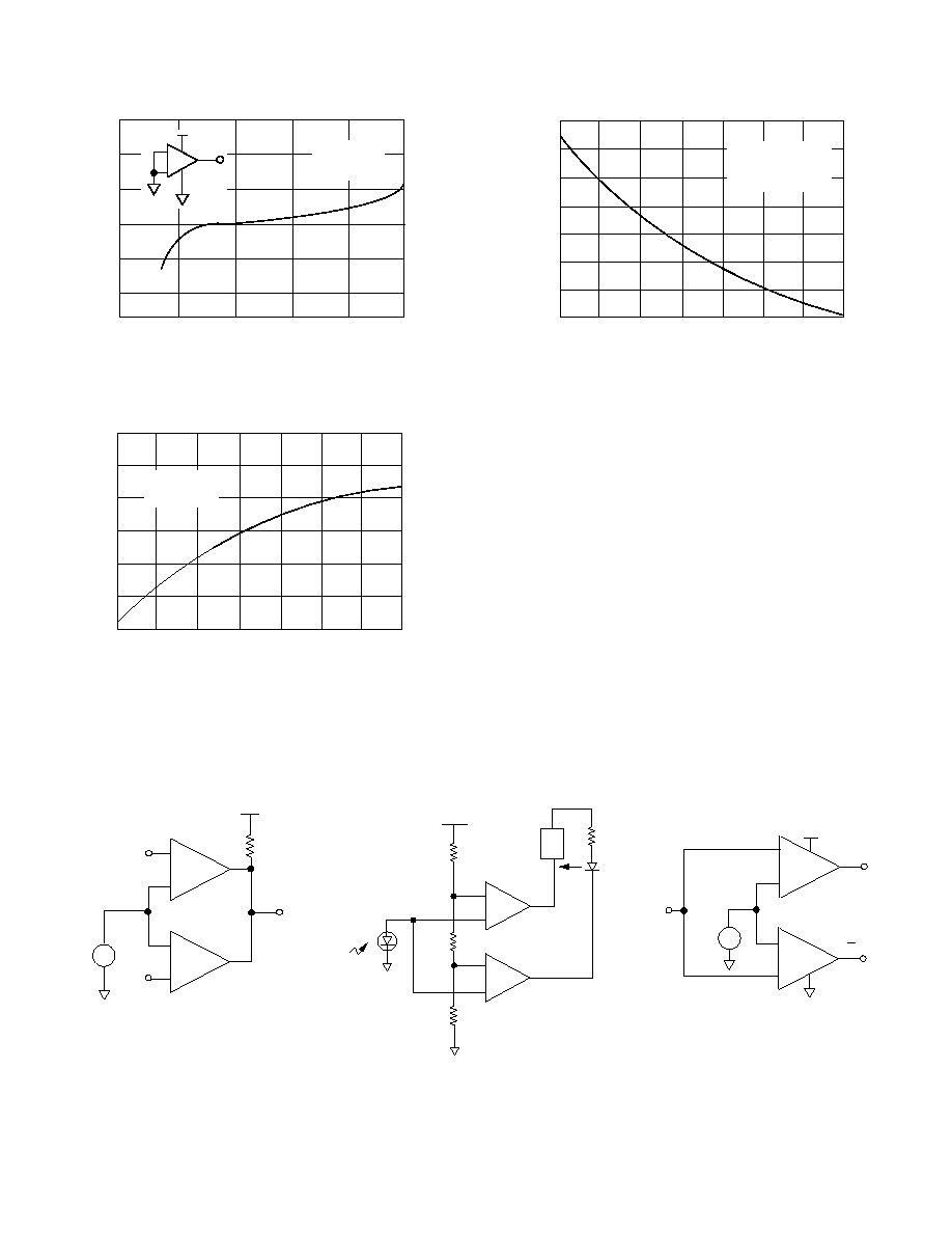
TYPICAL PERFORMANCE CHARACTERISTICS
120
100
80
60
140
0
25
50
75
-25
-55
TEMPERATURE (
∞
C)
SUPPLY CURRENT (
µ
A)
100
160
180
200
125
V
S
=
±
2.5V
No Load
All comparators
SUPPLY CURRENT vs. TEMPERATURE
2.4
2.2
2.0
1.8
2.6
0
25
50
75
-25
-55
TEMPERATURE (
∞
C)
OFFSET VOLTAGE (mV)
100
2.8
3.0
125
V
CM
= 0V
V
S
=
±
2.5V
INPUT OFFSET VOLTAGE vs.
TEMPERATURE
TYPICAL APPLICATIONS
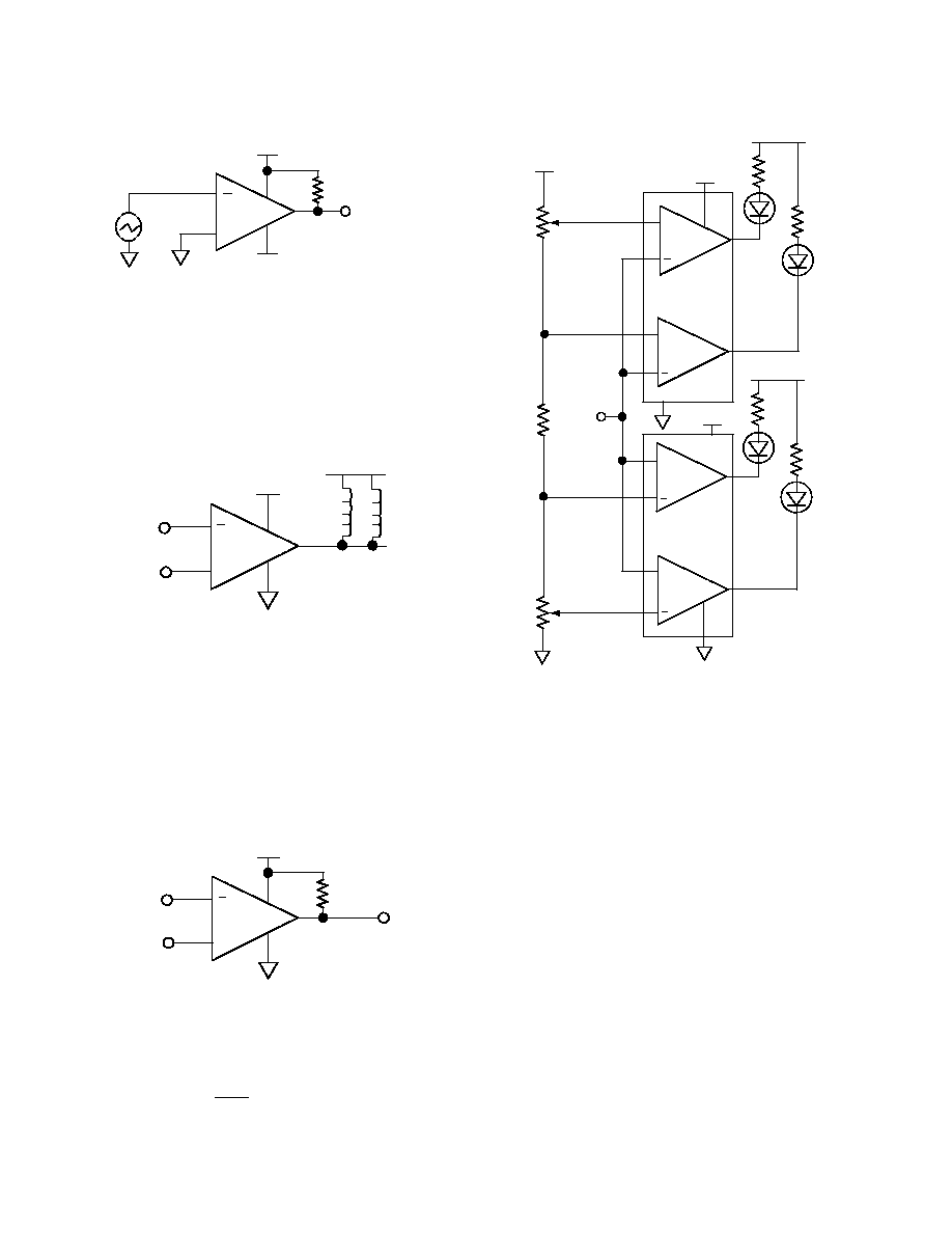
QUAD LIMIT WINDOW COMPARATOR
LED turns on as photo-detector voltage
reaches V
LIMIT1.
Both LED and horn turns on
as photo-detector voltage reaches V
LIMIT2.
V
EXTERNAL
= +12V V+ = +5V.
QUAD LIMIT PHOTO-DETECTOR
MONITOR
VOLTAGE COMPARATOR WITH
COMPLEMENTARY OUTPUTS
V+
V
LIMIT2
PHOTO-
DETECTOR
LIGHT
-
-
+
+
LED
BUZZER
V
LIMIT 1
V
External
1/2 ALD4301
1/2 ALD4301
+
+
-
-
1/2 ALD4301
OUTPUT HIGH FOR VIN < VREF(HIGH)
MINIMUM RLOAD
= 1.5K
>
AND
VOUT
VIN
V+
VREF(HIGH)
1/2 ALD4301
VREF(LOW)
VREF(LOW)
RLOAD
VIN
-
-
+
+
Q
Q
VIN
VREF
V+
1/2 ALD4301
1/2 ALD4301
140
120
100
80
160
6.0
8.0
10.0
12.0
4.0
2.0
SUPPLY VOLTAGE (V)
SUPPLY CURRENT (
µ
A)
T
A
= 25
∞
C
R
L
=
-
+
V +
TOTAL SUPPLY CURRENT vs.
TOTAL SUPPLY VOLTAGE