 | –≠–ª–µ–∫—Ç—Ä–æ–Ω–Ω—ã–π –∫–æ–º–ø–æ–Ω–µ–Ω—Ç: 5140 | –°–∫–∞—á–∞—Ç—å:  PDF PDF  ZIP ZIP |

5140
PROTECTED P
OWER
H
ALLÆ
SENSOR:
LAMP/SOLENOID DRIVER
The UGQ5140K unipolar Hall effect switch is a monolithic
integrated circuit designed for magnetic actuation of low-power
incandescent lamps or inductive loads such as relays or solenoids.
Included on chip is a Darlington power output that is capable of con-
tinuously sinking in excess of 300 mA. Internal protection circuitry
limits surge (lamp turn-ON) or fault currents to approximately 900 mA.
A sensitive magnetic threshold allows the device to be used in con-
junction with inexpensive magnets or in applications that require
relatively large operating distances.
Each sensor/driver includes a magnetic sensing Hall voltage
generator, operational amplifier, Schmitt trigger, voltage regulator, and
an open-collector, high-gain Darlington power output stage. The
regulator allows use of the device with supply voltages of 4.5 V to
28 V. On-chip compensation circuitry stabilizes switch-point perfor-
mance over temperature. The magnetic operation of this device is
similar to that of the A3141E-- Hall-effect switch.
The sensitive magnetic switch point coupled with the power output,
current limiting, and thermal limiting circuitry allow the UGQ5140K to
magnetically actuate various loads without requiring any external
components.
The UGQ5140K is rated for operation over an extended tempera-
ture range of -40
∞
C to +85
∞
C. It is supplied in a four-pin mini-SIP
plastic package, 0.200" (5.08 mm) wide, 0.130" (3.30 mm) high, and
0.060" (1.54 mm) thick.
FEATURES
s
Magnetically Actuated Power Switch
s
Temperature-Compensated Switch Points
s
High Current-Sink Capability
300 mA Continuous
900 mA Peak Current Limit
s
Output Short-Circuit Protection
s
Low Quiescent Standby Current
s
Linear Thermal Limiting
s
Automotive Temperature Range
-40
∞
C to +85
∞
C, Operating
s
Internal Inductive Flyback/Clamp Diode Protection
s
Reverse Battery Protection
s
Low-Profile 4-Pin Mini-SIP
5140
PROTECTED P
OWER
H
ALLÆ
SENSOR
-- LAMP/SOLENOID DRIVER
Always order by complete part number: UGQ5140K .
Pinning is shown viewed from branded side.
Dwg. PH-001
X
1
SUPPLY
V
CC
GROUND
DIODE
OUTPUT
2
3
4
Data Sheet
27695*
ABSOLUTE MAXIMUM RATINGS
at T
A
= +25
∞
C
Supply Voltage, V
CC
. . . . . . . . . . . . . . 28 V
Reverse Battery Voltage, V
RCC
. . . . . -45 V
Output OFF Voltage, V
OUT
. . . . . . . . . . 45 V
Over-Current Protected Output Voltage,
V
OUT
. . . . . . . . . . . . . . . . . . . . . . . . 25 V
Output ON Current, I
OUT
. . . . . . . 900 mA*
Magnetic Flux Density, B . . . . . . Unlimited
Package Power Dissipation,
P
D
. . . . . . . . . . . . . . . . . . . . See Graph
Operating Temperature Range,
T
A
. . . . . . . . . . . . . . . . . -40
∞
C to +85
∞
C
Storage Temperature Range,
T
S
. . . . . . . . . . . . . . . . -65
∞
C to +150
∞
C
* Output is current limited at approximately 900
mA and junction temperature limited if current in
excess of 900 mA is attempted. See Circuit
Description and Applications for further
information.
5140
PROTECTED P
OWER
H
ALLÆ
SENSOR:
LAMP/SOLENOID DRIVER
115 Northeast Cutoff, Box 15036
Worcester, Massachusetts 01615-0036 (508) 853-5000
Limits
Characteristic
Symbol
Test Conditions
Min.
Typ.
Max.
Units
Supply Voltage Range
V
CC
Operating
4.5
12
24
V
Output Leakage Current
I
OUT
V
OUT
= 24 V
--
<1.0
10
µ
A
Output Sustaining Voltage
V
OUT(SUS)
I
OUT
= 100 mA
35
--
--
V
Output Saturation Voltage
V
OUT(SAT)
I
OUT
= 300 mA, V
CC
= 24 V
--
0.84
1.2
V
Over-Current Limit
I
LIMIT
V
CC
= V
OUT
= 12 V, B
500 G
--
900
--
mA
Output Rise Time
t
r
V
CC
= 12 V, V
BB
= 18 V,
--
0.04
2.0
µ
s
Output Fall Time
t
f
R
L
= 1.1 k
, C
L
= 20 pF
--
0.04
2.0
µ
s
Supply Current
I
CC
Output OFF
--
5.5
10
mA
Diode Forward Voltage
V
F
I
F
= 300 mA
--
1.1
1.5
V
Diode Leakage Current
I
R
V
R
= 35 V
--
<1.0
50
µ
A
Thermal Limit
T
LIMIT
V
CC
= V
OUT
= 12 V, B
500 G,
I
OUT
= 10 mA
--
165
--
∞
C
T
A
= +25
∞
C
T
A
= -40
∞
C to +85
∞
C
Characteristic
Symbol
Min.
Typ.
Max.
Min.
Typ.
Max.
Units
Magnetic Operate Point
B
OP
70
155
200
45
--
240
G
Magnetic Release point
B
RP
50
100
180
25
--
220
G
Hysteresis
B
hys
20
55
--
20
--
--
G
Typical Data is at T
A
= +25
∞
C and is for design information only.
50
75
100
125
150
1.0
0.2
0
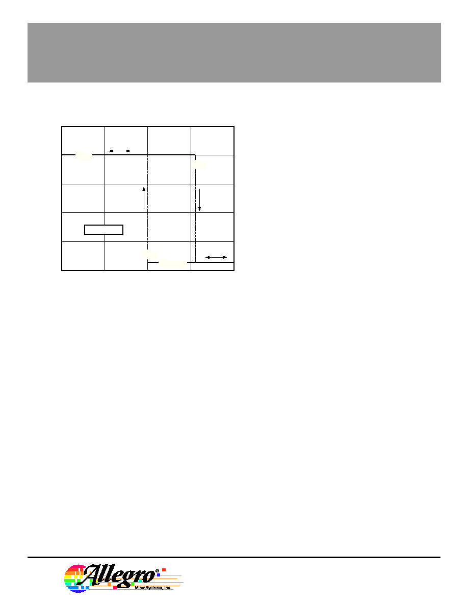
ALLOWABLE PACKAGE POWER DISSIPATION IN WATTS
AMBIENT TEMPERATURE IN
∞
C
0.8
0.6
0.4
25
Dwg. GH-001
0
-25
FREE AIR, R = 177
∞
C/W
JA
-50
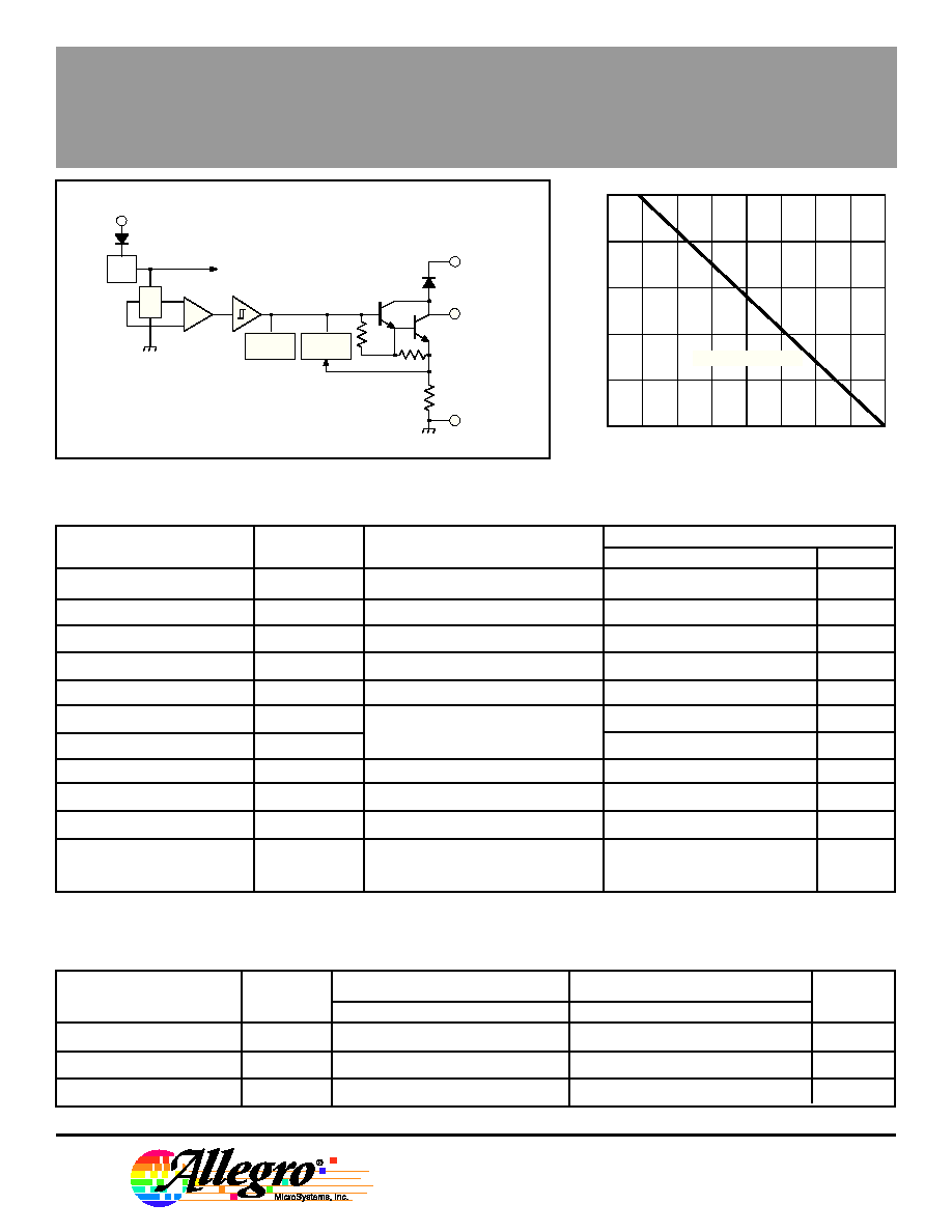
REG.
1
V
CC
REV. BATTERY
PROTECTION
Dwg. FH-001
DIODE
OUTPUT
GROUND
3
<<1
THERMAL
LIMIT
CURRENT
LIMIT
X
2
4
W
Copyright © 1991, 1995 Allegro MicroSystems, Inc.
FUNCTIONAL BLOCK DIAGRAM
ELECTRICAL CHARACTERISTICS at T
A
= -40
∞
C to +85
∞
C, V
CC
= 4.5 V to 24 V
(unless otherwise noted).
MAGNETIC CHARACTERISTICS at V
CC
= 4.5 V to 24 V.

5140
PROTECTED P
OWER
H
ALLÆ
SENSOR:
LAMP/SOLENOID DRIVER
TYPICAL OPERATING CHARACTERISTICS
-20
0
25
55
85
180
100
AMBIENT TEMPERATURE IN
∞
C
160
140
120
-40
Dwg. GH-006A
I = 10 mA
OUT
80
SWITCH POINT IN GAUSS
OPERATE POINT
RELEASE POINT
-20
0
25
55
85
1.0
0.6
AMBIENT TEMPERATURE IN
∞
C
0.9
0.8
0.7
-40
Dwg. GH-002A
SATURATION VOLTAGE IN VOLTS
I = 300 mA
OUT
-20
0
25
55
85
9.0
5.0
AMBIENT TEMPERATURE IN
∞
C
8.0
7.0
6.0
-40
Dwg. GH-003A
SUPPLY CURRENT IN mA
OUTPUT ON
I = 10 mA
OUT
OUTPUT OFF
V = 12 V
CC
25
85
105
125
1000
800
AMBIENT TEMPERATURE IN
∞
C
950
900
0
Dwg. GH-004
-20
-40
850
750
55
PEAK CURRENT LIMIT IN mA
5140
PROTECTED P
OWER
H
ALLÆ
SENSOR:
LAMP/SOLENOID DRIVER
115 Northeast Cutoff, Box 15036
Worcester, Massachusetts 01615-0036 (508) 853-5000
TYPICAL TRANSFER CHARACTERISTICS
at T
A
= +25
∞
C
100
125
150
175
200
3.0
0
OUTPUT VOLTAGE IN VOLTS
MAGNETIC FLUX DENSITY IN GAUSS
12
9.0
6.0
75
Dwg. GH-007
50
25
0
15
I = 300 mA
OUT
B
OP
B
RP
V
OUT(SAT)
V
B B
CIRCUIT DESCRIPTION AND OP-
ERATION
The UGQ5140K merges state-of-the-art
Hall effect sensing and power driving tech-
nologies to allow precision non-contact
actuation of incandescent lamps or inductive
loads. It is rated for operation over an
extended temperature range as typically
required in automotive applications.
MAGNETIC OPERATION
As shown in the Transfer Characteristics
graph, the output of the device (pin 2)
switches low when the magnetic field at the
Hall sensor exceeds the operate point
threshold (B
OP
). At this point, the output
voltage is V
OUT(SAT)
. When the magnetic field
is reduced to below the release point thresh-
old (B
RP
), the device output goes high. The
difference in the magnetic operate and
release points is called the hysteresis (B
H
) of
the part. This built-in hysteresis allows clean
switching of the output even in the presence
of external mechanical vibration and electri-
cal noise.
CURRENT AND THERMAL
LIMITING
Output short circuits may be caused by
faulty connectors, crimped wiring harnesses,
or blown loads. In such cases, current and
thermal limit circuitry will protect the output
transistor against destruction.
Current through the output transistor is
sensed with a low-value on-chip aluminum
resistor. The voltage drop across this
resistor is fed back to control the base drive
of the output stage. This feedback prevents
the output transistor from exceeding its
maximum current density rating by limiting
the output current to approximately 900 mA.
It may also cause the output voltage to
increase (V
OUT
= V
BB
- [I
LIMIT
x R
L
]). In this
mode, the device will dissipate an increased
amount of power (P
D
= V
OUT
x I
LIMIT
) and the
output transistor will be thermally stressed.
5140
PROTECTED P
OWER
H
ALLÆ
SENSOR:
LAMP/SOLENOID DRIVER
This stress, unless protected against (as in the
UGQ5140K), will cause the device junction tempera-
ture to rise until it fails catastrophically.
Thermal stress protection is provided in two
manners; delta temperature protection, and junction
temperature protection. Under worst-case conditions
(see Figures 1 and 2), if the output is shorted to
supply, the output transistor will heat up much faster
than the rest of the integrated circuit. This condition
could cause localized failure in the output transistor.
To prevent damage, a delta temperature limiting
scheme is used. If a large thermal gradient is sensed
across the device, the output transistor base drive is
reduced to lower the output current. This reduces the
power (heat) generated by the output transistor.
When thermal stresses cause the junction tem-
perature to reach approximately +165
∞
C, a linear
thermal limiting circuit is activated. This circuit linearly
reduces the base drive of the output transistor to
maintain a constant junction temperature of 165
∞
C. In
this mode, the output current will be a function of the
heat dissipating characteristics of the package and its
environment. Linear thermal limiting eliminates the
low-frequency thermal oscillation problems experi-
enced by thermal shutdown (ON-OFF) schemes.
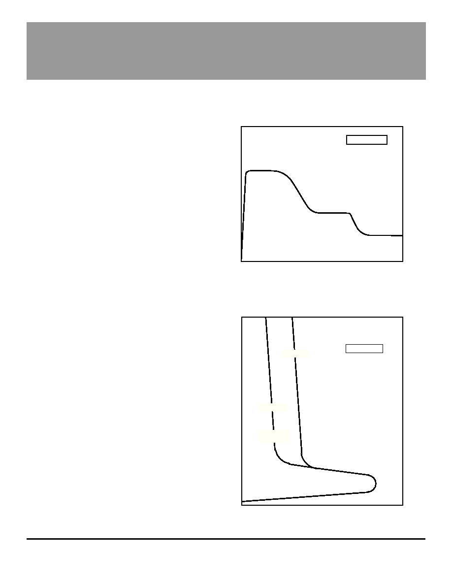
The output characteristics are shown in Figures 1
and 2. Note the three distinct operating regions: peak
limit, delta limit, and thermal limit. In practice the
output voltage and current may exhibit some oscilla-
tions during peak current limiting due to output load
characteristics. These oscillations are of very-short
duration (typically 50 ms) and may be damped with an
external capacitor between pins 2 and 4.
When the fault condition that caused the output
overload is corrected, the device returns to normal
operating mode.
FIGURE 1
OUTPUT CURRENT UNDER SHORT-CIRCUIT
CONDITIONS
FIGURE 2
OUTPUT VOLTAGE vs OUTPUT CURRENT
TIME
Dwg. WH-002
OUTPUT CURRENT
PEAK CURRENT LIMIT
JUNCTION
TEMP. LIMIT
DELTA TEMP.
LIMIT
NOT TO SCALE
V
OUT(SAT)
Dwg. GP-013-1
OUTPUT VOLTAGE, V
OUT
OUTPUT CURRENT, I
OUT
T < 150
∞
C
T = 165
∞
C
J
J
DELTA
TEMP. LIMIT
CURRENT LIMIT
JUNCTION
TEMP. LIMIT
NOT TO SCALE