Data
Sheet
26180.120
8-BIT LATCHED
DMOS POWER DRIVER
The A6273KA and A6273KLW combine eight (positive-edge-
triggered D-type) data latches and DMOS outputs for systems requiring
relatively high load power. Driver applications include relays, sole-
noids, and other medium-current or high-voltage peripheral power loads.
The CMOS inputs and latches allow direct interfacing with microproces-
sor-based systems. Use with TTL may require appropriate pull-up
resistors to ensure an input logic high.
The DMOS output inverts the DATA input. All of the output
drivers are disabled (the DMOS sink drivers turned OFF) with the
CLEAR input low. The A6273KA/KLW DMOS open-drain outputs are
capable of sinking up to 750 mA. Similar devices with reduced r
DS(on)
will be available as the A6A273.
The A6273KA is furnished in a 20-pin dual in-line plastic package.
The A6273KLW is furnished in a 20-lead wide-body, small-outline
plastic package (SOIC) with gull-wing leads for surface-mount applica-
tions. Copper lead frames, reduced supply current requirements, and
low on-state resistance allow both devices to sink 150 mA from all
outputs continuously, to ambient temperatures over 85
�C.
FEATURES
I 50 V Minimum Output Clamp Voltage
I 250 mA Output Current (all outputs simultaneously)
I 1.3 Typical
r
DS(on)
I Low Power Consumption
I Replacements for TPIC6273N and TPIC6273DW
6273
ADVANCE INFORMATION
(Subject to change without notice)
January 24, 2000
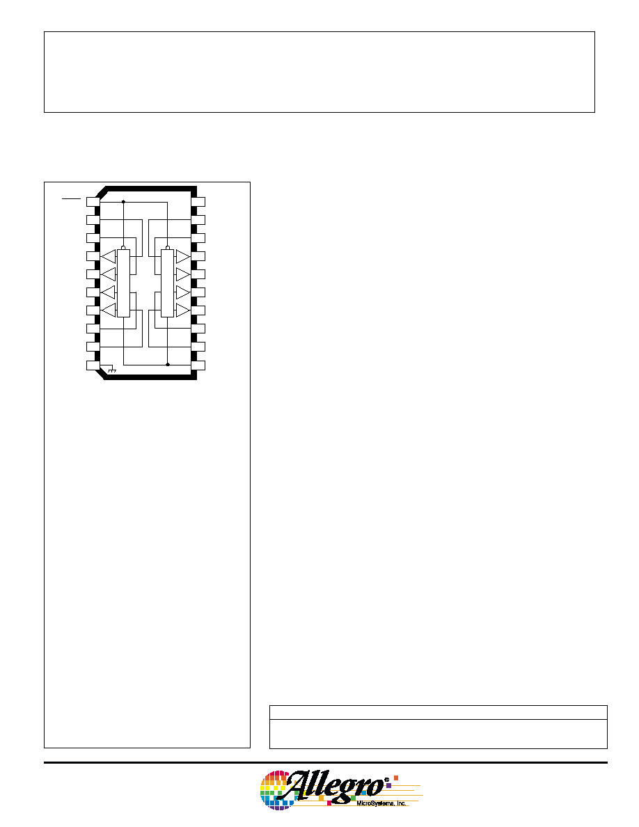
Note that the A6273KA (DIP) and the A6273KLW
(SOIC) are electrically identical and share a com-
mon terminal number assignment.
1
2
3
8
9
13
14
15
16
17
19
4
5
6
7
12
18
20
IN
V
DD
GROUND
OUT
8
OUT
7
OUT
6
Dwg. PP-015-2
OUT
1
OUT
2
OUT
3
OUT
4
OUT
5
10
11
CLEAR
LOGIC
SUPPLY
STROBE
8
IN
7
IN
6
IN
5
IN
4
IN
3
IN
2
IN
1
LATCHES
LATCHES
Always order by complete part number:
Part Number
Package
R
JA
R
JC
A6273KA
20-pin DIP
55
�C/W
25
�C/W
A6273KLW
20-lead SOIC
70
�C/W
17
�C/W
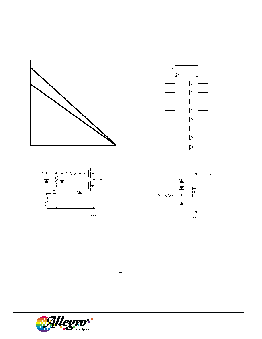
ABSOLUTE MAXIMUM RATINGS
at T
A
= 25
�
C
Output Voltage, V
O
............................. 50 V
Output Drain Current,
Continuous, I
O
....................... 250 mA*
Peak, I
OM
.............................. 750 mA*
Peak, I
OM
..................................... 2.0 A
Single-Pulse Avalanche Energy,
E
AS
.............................................. 75 mJ
Logic Supply Voltage, V
DD
................ 7.0 V
Input Voltage Range,
V
I
................................. -0.3 V to +7.0 V
Package Power Dissipation,
P
D
........................................ See Graph
Operating Temperature Range,
T
A
.............................. -40
�
C to +125
�
C
Storage Temperature Range,
T
S
.............................. -55
�
C to +150
�
C
* Each output, all outputs on.
Pulse duration
100 �s, duty cycle 2%.
Caution: These CMOS devices have input
static protection (Class 3) but are still
susceptible to damage if exposed to extremely
high static electrical charges.
6273
8-BIT LATCHED
DMOS POWER DRIVER
115 Northeast Cutoff, Box 15036
Worcester, Massachusetts 01615-0036 (508) 853-5000
Copyright � 2000, Allegro MicroSystems, Inc.
LOGIC SYMBOL
C1
R
1D
4
5
6
7
14
15
16
17
1
2
11
Dwg. FP-046-1
1D
3
1D
8
1D
9
1D
12
1D
13
1D
18
1D
19
50
75
100
125
150
2.5
0.5
0
ALLOWABLE PACKAGE POWER DISSIPATION IN WATTS
AMBIENT TEMPERATURE IN
�C
2.0
1.5
1.0
25
Dwg. GS-004A
SUFFIX 'LW', R = 70
�C/W
JA
SU
FF
IX
'A
', R
=
5
5�C
/W
JA
FUNCTION TABLE
Inputs
CLEAR
STROBE
IN
X
OUT
X
L
X
X
H
H
H
L
H
L
H
H
L
X
R
L = Low Logic Level
H = High Logic Level
X = Irrelevant
R = Previous State
DMOS POWER DRIVER OUTPUT
LOGIC INPUTS
IN
Dwg. EP-010-16
V
DD
Dwg. EP-063
OUT

6273
8-BIT LATCHED
DMOS POWER DRIVER
115 Northeast Cutoff, Box 15036
Worcester, Massachusetts 01615-0036 (508) 853-5000
Limits
Characteristic
Symbol
Test Conditions
Min.
Typ.
Max.
Units
Logic Supply Voltage
V
DD
Operating
4.5
5.0
5.5
V
Output Breakdown
V
(BR)DSX
I
O
= 1 mA
50
--
--
V
Voltage
Off-State Output
I
DSX
V
O
= 40 V
--
0.05
1.0
�A
Current
V
O
= 40 V T
A
= 125
�C
--
0.15
5.0
�A
Static Drain-Source
r
DS(on)
I
O
= 250 mA, V
DD
= 4.5 V
--
1.3
2.0
On-State Resistance
I
O
= 250 mA, V
DD
= 4.5 V, T
A
= 125
�C
--
2.0
3.2
I
O
= 500 mA, V
DD
= 4.5 V (see note)
--
1.3
2.0
Nominal Output
I
O(nom)
V
DS(on)
= 0.5 V, T
A
= 85
�C
--
250
--
mA
Current
Logic Input Current
I
IH
V
I
= V
DD
= 5.5 V
--
--
1.0
�A
I
IL
V
I
= 0, V
DD
= 5.5 V
--
--
-1.0
�A
Prop. Delay Time
t
PLH
I
O
= 250 mA, C
L
= 30 pF
--
625
--
ns
t
PHL
I
O
= 250 mA, C
L
= 30 pF
--
150
--
ns
Output Rise Time
t
r
I
O
= 250 mA, C
L
= 30 pF
--
675
--
ns
Output Fall Time
t
f
I
O
= 250 mA, C
L
= 30 pF
--
400
--
ns
Supply Current
I
DD(off)
V
DD
= 5.5 V, Outputs OFF
--
15
100
�A
I
DD(on)
V
DD
= 5.5 V, Outputs ON
--
150
300
�A
Typical Data is at V
DD
= 5 V and is for design information only.
NOTE -- Pulse test, duration
100 �s, duty cycle 2%.
ELECTRICAL CHARACTERISTICS at T
A
= +25
�
C, V
DD
= 5 V, t
ir
= t
if
10 ns (unless otherwise
specified).
RECOMMENDED OPERATING CONDITIONS
over operating temperature range
Logic Supply Voltage Range, V
DD
............... 4.5 V to 5.5 V
High-Level Input Voltage, V
IH
............................
0.85V
DD
Low-level input voltage, V
IL
.................................
0.15V
DD
6273
8-BIT LATCHED
DMOS POWER DRIVER
www.allegromicro.com
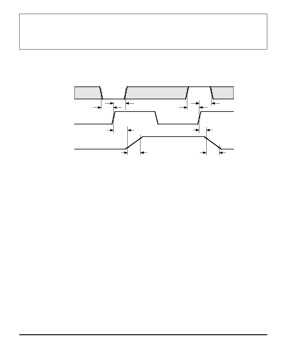
TIMING REQUIREMENTS
PHL
t
90%
f
t
50%
su(D)
t
PLH
t
50%
OUTPUTx
Dwg. WP-036-1
10%
r
t
INx
STROBE
h(D)
t
50%
su(D)
t
h(D)
t
Input Active Time Before Strobe
(Data Set-Up Time), t
su(D)
.............................................. 20 ns
Input Active Time After Strobe
(Data Hold Time), t
h(D)
................................................... 20 ns
Input Pulse Width, t
w(D)
...................................................... 40 ns
Input Logic High, V
IH
................................................
0.85V
DD
Input Logic Low, V
IL
.................................................
0.15V
DD
