DABiC-IV, 10-BIT SERIAL-INPUT,
LATCHED SOURCE DRIVERS
A6810xA
Data Sheet
26182.124B
ABSOLUTE MAXIMUM RATINGS
at T
A
= 25
∞
C
Logic Supply Voltage, V
DD
................... 7.0 V
Driver Supply Voltage, V
BB
................... 60 V
Continuous Output Current Range,
I
OUT
......................... -40 mA to +15 mA
Input Voltage Range,
V
IN
....................... -0.3 V to V
DD
+ 0.3 V
Package Power Dissipation,
P
D
........................................ See Graph
Operating Temperature Range, T
A
(Suffix `E≠') .................. -40
∞
C to +85
∞
C
(Suffix `S≠') .................. -20
∞
C to +85
∞
C
Storage Temperature Range,
T
S
............................... -55
∞
C to +125
∞
C
Caution: These CMOS devices have input
static protection (Class 2) but are still
susceptible to damage if exposed to
extremely high static electrical charges.
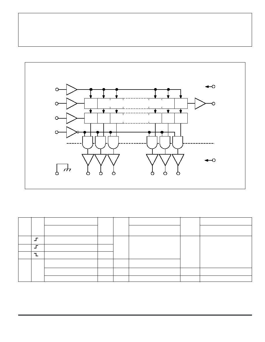
The A6809≠ and A6810≠ devices combine 10-bit CMOS shift
registers, accompanying data latches and control circuitry with bipolar
sourcing outputs and pnp active pull downs. Designed primarily to
drive vacuum-fluorescent displays, the 60 V and -40 mA output ratings
also allow these devices to be used in many other peripheral power
driver applications. The A6809≠ and A6810≠ feature an increased data
input rate (compared with the older UCN/UCQ5810-F) and a con-
trolled output slew rate. The A6809xLW and A6810xLW are identical
except for pinout.
The CMOS shift register and latches allow direct interfacing with
microprocessor-based systems. With a 3.3 V or 5 V logic supply,
typical serial-data input rates are up to 33 MHz.
A CMOS serial data output permits cascade connections in applica-
tions requiring additional drive lines. Similar devices are avail-able as
the A6811≠ (12 bits), A6812≠ (20 bits), and A6818≠ (32 bits).
The A6809≠ and A6810≠ output source drivers are npn Darling-
tons, capable of sourcing up to 40 mA. The controlled output slew rate
reduces electromagnetic noise, which is an important consideration in
systems that include telecommunications and/or microprocessors and
to meet government emissions regulations. For inter-digit blanking, all
output drivers can be disabled and all sink drivers turned on with a
BLANKING input high. The pnp active pull-downs will sink at least
2.5 mA.
All devices are available in two temperature ranges for optimum
performance in commercial (suffix S-) or industrial (suffix E-) applica-
tions. The A6810≠ is provided in three package styles for through-hole
DIP (suffix -A), surface-mount SOIC (suffix -LW), or minimum-area
surface-mount PLCC (suffix -EP). The A6809≠ is provided in the
SOIC (suffix -LW) only. Copper lead frames, low logic-power dissi-
pation, and low output-saturation voltages allow all devices to source
25 mA from all outputs continuously over the maximum operating
temperature range.
FEATURES
I Controlled Output Slew Rate
I High-Speed Data Storage
I 60 V Minimum
Output Breakdown
I High Data Input Rate
I PNP Active Pull-Downs
Complete part number includes a suffix to identify operating
temperature range (E- or S-) and package type (-A, -EP, or -LW).
Always order by complete part number, e.g., A6810SLW .
6809
AND
6810
I Low Output-Saturation Voltages
I Low-Power CMOS Logic
and Latches
I Improved Replacements
for TL4810≠, UCN5810≠,
and UCQ5810≠
2
3
4
5
6
7
8
9
10
11
12
13
14
15
16
17
18
SERIAL
DATA OUT
LOAD
SUPPLY
SERIAL
DATA IN
BLANKING
LOGIC
SUPPLY
STROBE
GROUND
CLOCK
CLK
V
ST
BLNK
DD
BB
V
OUT
9
OUT
10
OUT
1
OUT
2
OUT
3
Dwg. PP-029
OUT
8
OUT
7
OUT
6
OUT
5
OUT
4
1
LATCHES
REGISTER
REGISTER
LATCHES

6809
AND
6810
10-BIT SERIAL-INPUT,
LATCHED SOURCE DRIVERS
115 Northeast Cutoff, Box 15036
Worcester, Massachusetts 01615-0036 (508) 853-5000
Limits @ V
DD
= 3.3 V Limits @ V
DD
= 5 V
Characteristic
Symbol
Test Conditions
Mln.
Typ.
Max.
Min.
Typ.
Max.
Units
Output Leakage Current
I
CEX
V
OUT
= 0 V
--
<-0.1
-15
--
<-0.1
-15
µA
Output Voltage
V
OUT(1)
I
OUT
= -25 mA
57.5
58.3
--
57.5
58.3
--
V
V
OUT(0)
I
OUT
= 1 mA
--
1.0
1.5
--
1.0
1.5
V
Output Pull-Down Current
I
OUT(0)
V
OUT
= 5 V to V
BB
2.5
5.0
--
2.5
5.0
--
mA
Input Voltage
V
IN(1)
2.2
--
--
3.3
--
--
V
V
IN(0)
--
--
1.1
--
--
1.7
V
Input Current
I
IN(1)
V
IN
= V
DD
--
<0.01
1.0
--
<0.01
1.0
µA
I
IN(0)
V
IN
= 0 V
--
<-0.01
-1.0
--
<-0.01
-1.0
µA
Input Clamp Voltage
V
IK
I
IN
= -200
µA
--
-0.8
-1.5
--
-0.8
-1.5
V
Serial Data Output Voltage
V
OUT(1)
I
OUT
= -200
µA
2.8
3.05
--
4.5
4.75
--
V
V
OUT(0)
I
OUT
= 200
µA
--
0.15
0.3
--
0.15
0.3
V
Maximum Clock Frequency
f
c
10
33
--
10
33
--
MHz
Logic Supply Current
I
DD(1)
All Outputs High
--
0.25
0.75
--
0.3
1.0
mA
I
DD(0)
All Outputs Low
--
0.25
0.75
--
0.3
1.0
mA
Load Supply Current
I
BB(1)
All Outputs High, No Load
--
1.5
3.0
--
1.5
3.0
mA
I
BB(0)
All Outputs Low
--
0.2
20
--
0.2
20
µA
Blanking-to-Output Delay
t
dis(BQ)
C
L
= 30 pF, 50% to 50%
--
0.7
2.0
--
0.7
2.0
µs
t
en(BQ)
C
L
= 30 pF, 50% to 50%
--
1.8
3.0
--
1.8
3.0
µs
Strobe-to-Output Delay
t
p(STH-QL)
R
L
= 2.3 k
, C
L
30 pF
--
0.7
2.0
--
0.7
2.0
µs
t
p(STH-QH)
R
L
= 2.3 k
, C
L
30 pF
--
1.8
3.0
--
1.8
3.0
µs
Output Fall Time
t
f
R
L
= 2.3 k
, C
L
30 pF
2.4
--
12
2.4
--
12
µs
Output Rise Time
t
r
R
L
= 2.3 k
, C
L
30 pF
2.4
--
12
2.4
--
12
µs
Output Slew Rate
dV/dt
R
L
= 2.3 k
, C
L
30 pF
4.0
--
20
4.0
--
20
V/
µs
Clock-to-Serial Data Out Delay t
p(CH-SQX)
I
OUT
=
±200 µA
--
50
--
--
50
--
ns
Negative current is defined as coming out of (sourcing) the specified device terminal.
Typical data is is for design information only and is at T
A
= +25
∞C.
ELECTRICAL CHARACTERISTICS at T
A
= +25
∞
C (A6809SLW & A6810S-) or over operating
temperature range (A6809ELW & A6810E-), V
BB
= 60 V unless otherwise noted.
6809
AND
6810
10-BIT SERIAL-INPUT,
LATCHED SOURCE DRIVERS
www.allegromicro.com
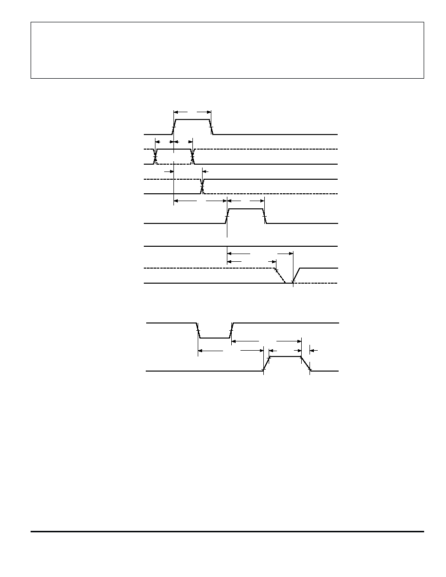
TIMING REQUIREMENTS and SPECIFICATIONS
(Logic Levels are V
DD
and Ground)
Serial Data present at the input is transferred to the shift
register on the logic "0" to logic "1" transition of the CLOCK
input pulse. On succeeding CLOCK pulses, the registers shift
data information towards the SERIAL DATA OUTPUT. The
SERIAL DATA must appear at the input prior to the rising edge
of the CLOCK input waveform.
Information present at any register is transferred to the
respective latch when the STROBE is high (serial-to-parallel
conversion). The latches will continue to accept new data as
long as the STROBE is held high. Applications where the
latches are bypassed (STROBE tied high) will require that the
BLANKING input be high during serial data entry.
When the BLANKING input is high, the output source
drivers are disabled (OFF); the pnp active pull-down sink
drivers are ON. The information stored in the latches is not
affected by the BLANKING input. With the BLANKING input
low, the outputs are controlled by the state of their respective
latches.
CLOCK
SERIAL
DATA IN
STROBE
BLANKING
OUT
N
Dwg. WP-029
50%
SERIAL
DATA OUT
DATA
DATA
10%
90%
50%
50%
50%
C
A
B
D
E
LOW = ALL OUTPUTS ENABLED
p(STH-QL)
t
p(CH-SQX)
t
DATA
p(STH-QH)
t
BLANKING
OUT
N
Dwg. WP-030
DATA
10%
50%
en(BQ)
t
dis(BQ)
t
HIGH = ALL OUTPUTS BLANKED (DISABLED)
90%
r
t
f
t
A. Data Active Time Before Clock Pulse
(Data Set-Up Time), t
su(D)
......................................... 25 ns
B. Data Active Time After Clock Pulse
(Data Hold Time), t
h(D)
............................................... 25 ns
C. Clock Pulse Width, t
w(CH)
............................................... 50 ns
D. Time Between Clock Activation and Strobe, t
su(C)
....... 100 ns
E. Strobe Pulse Width, t
w(STH)
............................................. 50 ns
NOTE ≠ Timing is representative of a 10 MHz clock. Signifi-
cantly higher speeds are attainable.