6817
ADDRESSABLE
28-LINE
DECODER/DRIVER
6
5
4
3
2
1
44
43
42
41
40
7
8
9
10
11
12
13
14
15
16
17
29
30
39
38
37
36
35
34
33
32
31
28
27
26
25
24
23
22
21
20
19
18
Dwg. PP-050
IN
C
GND
IC
GND
IC
IC
CHIP ENABLE
LOGIC SUPPLY
GND
GND
IN
B
4-TO-14 LINE DECODER
OUTPUT DRIVER BANK A
OUTPUT DRIVER BANK B
OUT
B0
NC
OUTA9
OUTA8
OUTA7
OUTA6
OUTA5
OUTA4
OUTA3
OUTA2
OUTA1
OUTA0
OUTB1
OUTB2
OUTB3
OUTB4
OUTB5
OUTB6
OUTB7
OUTB8
OUTB9
OUTPUT ENABLE
B
OUTPUT ENABLE
A
OUT
B10
OUT
B11
OUT
B12
OUT
B13
OUT
A13
OUT
A12
OUT
A11
OUT
A10
V
DD
IN (MSB)
D
IN (LSB)
A
Always order by complete part number: A6817SEP .
ADDRESSABLE
28-LINE DECODER/DRIVER
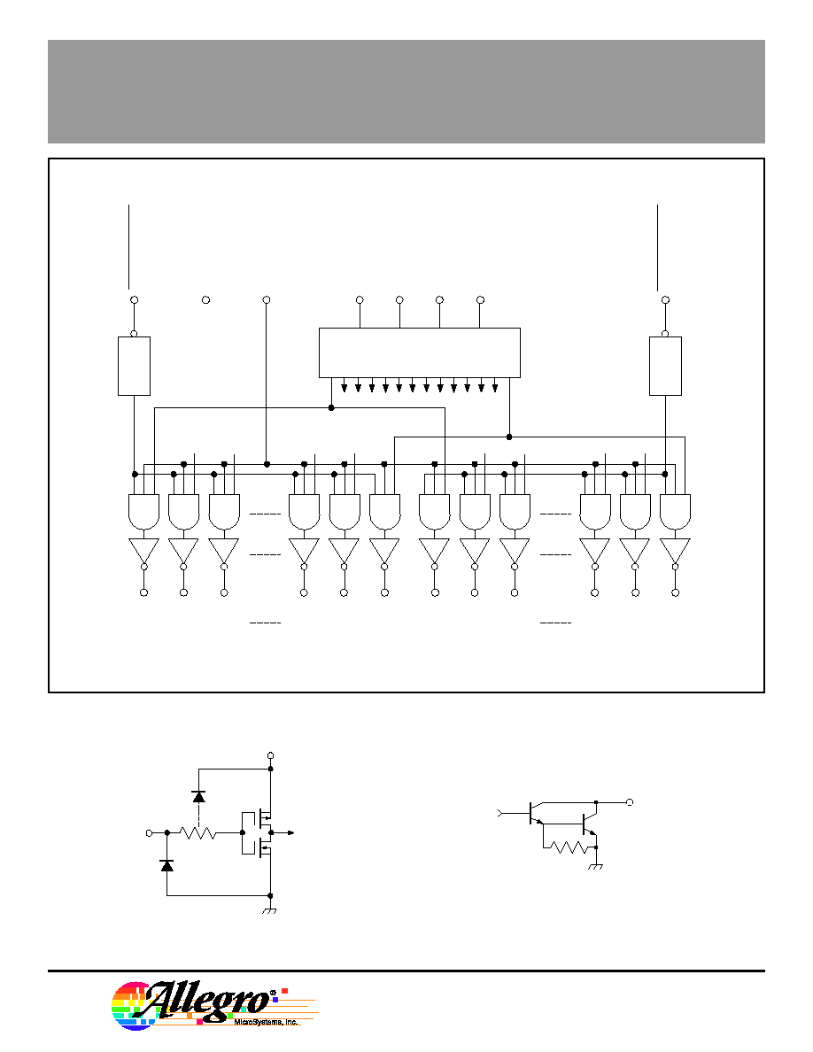
Intended for use in ink-jet printer applications, the A6817SEP
addressable 28-line decoder/driver combines low-power CMOS inputs
and logic with 28 high-current, high-voltage bipolar outputs. A 4-to-14
line decoder determines the selected output driver (n) in each
14-driver bank. Two independent output-enable inputs (active low)
then provide the final decoding to activate 1- or 2-of-28 outputs
(OUT
An
and/or OUT
Bn
). Special internal circuitry is programmed at the
time of manufacture to adjust the output pulse timing and thereby the
energy the device delivers to the ink-jet print head. The DABiC-IV
A6817SEP directly replaces the original BiMOS-II A5817SEP in most
applications.
The CMOS inputs cause minimal loading and are compatible with
standard CMOS, PMOS, and NMOS logic. Use with TTL or DTL
circuits may require appropriate pull-up resistors to ensure an input
logic high. The internal CMOS logic operates from a 5 V supply.
A CHIP ENABLE function is provided to lock out the drivers during
system power up. The 28 bipolar power outputs are open-collector
30 V Darlington drivers capable of sinking 500 mA at ambient
temperatures up to 85
�
C.
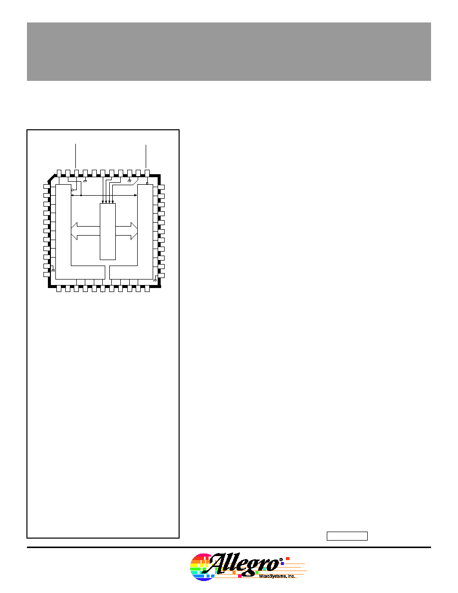
The A6817SEP is furnished in a 44-lead plastic chip carrier
(quad pack) for minimum-area, surface-mount applications.
FEATURES
s
Controlled Characteristics for Ink-Jet Printers
s
Addressable Data Entry
s
30 V Minimum V
(BR)CEX
s
CMOS, PMOS, NMOS Compatible Inputs
s
Low-Power CMOS Logic
ABSOLUTE MAXIMUM RATINGS
at T
A
= 25
�
C
Output Voltage, V
CE
............................. 30 V
Logic Supply Voltage, V
DD
.................. 7.0 V
Input Voltage Range,
V
IN
....................... -0.3 V to V
DD
+ 0.3 V
Output Current, I
C
........................... 600 mA
Package Power Dissipation, P
D
..... 2.70 W*
Operating Temperature Range,
T
A
................................. -20
�
C to +85
�
C
Storage Temperature Range,
T
S
.............................. -55
�
C to +150
�
C
*Derate at rate of 22 mW/
�
C above T
A
= 25
�
C.
Caution: These CMOS devices have input static
protection (Class 2) but are still susceptible to
damage when exposed to extremely high static
electrical charges.
6817
Data Sheet
26186.22
6817
ADDRESSABLE
28-LINE
DECODER/DRIVER
115 Northeast Cutoff, Box 15036
Worcester, Massachusetts 01615-0036 (508) 853-5000
Dwg. FP-032
4-TO-14 LINE DECODER
CHIP ENABLE
IN (MSB)
D
IN (LSB)
A
IN
B
IN
C
LOGIC SUPPLY
OUTPUT ENABLE
A
OUTPUT ENABLE
B
OUT
A0
OUT
A1
OUT
A2
OUT
A11
OUT
A12
OUT
A13
OUT
B0
OUT
B1
OUT
B2
OUT
B11
OUT
B12
OUT
B13
TURN-ON
DELAY
TURN-ON
DELAY
FUNCTIONAL BLOCK DIAGRAM
TYPICAL INPUT CIRCUIT
TYPICAL OUTPUT DRIVER
Dwg. EP-010-1
IN
V
DD
Dwg. EP-021-7
OUTN
W
Copyright � 1997, Allegro MicroSystems, Inc.
6817
ADDRESSABLE
28-LINE
DECODER/DRIVER
ELECTRICAL CHARACTERISTICS at T
A
= +25
�
C, V
DD
= 5.0 V.
Limits
Characteristic
Symbol
Test Conditions
Min
Typ
Max
Units
Output Drivers
Output Leakage Current
I
CEX
V
CE
= 30 V
--
<1.0
100
�
A
Output Saturation Voltage
V
CE(SAT)
I
OUT
= 450 mA
0.80
1.10
1.40
V
I
OUT
= 400 mA
0.75
1.05
1.35
V
Output Breakdown Voltage
V
(BR)CEX
R
L
= 56
30
--
--
V
Unclamped Inductive
--
V
CC
= 30 V, L = 3
�
H, R
L
= 56
,
See Note
--
Load Current
I
L
= 500 mA, Test Fig.
Turn-On Time
t
PHL
V
CC
= 21 V, R
L
= 39
25
100
425
ns
Fall Time
t
f
V
CC
= 21 V, R
L
= 39
--
20
--
ns
Turn-Off Time
t
PLH
V
CC
= 21 V, R
L
= 39
50
125
350
ns
Rise Time
t
r
V
CC
= 21 V, R
L
= 39
--
50
--
ns
Control Logic
Logic Input Voltage
V
IN(1)
3.5
--
--
V
V
IN(0)
--
--
0.8
V
Logic Input Current
I
IN(1)
V
IN
= 5.0 V
--
<1.0
100
�
A
I
IN(0)
V
IN
= 0 V
--
<-1.0
-100
�
A
Input Resistance
R
IN
50
--
--
k
Supply Current
I
DD(ON)
Two Outputs ON
--
6.0
10.0
mA
I
DD(OFF)
All Drivers OFF, All Inputs = 0 V,
--
--
600
�
A
OE
A
= OE
B
= V
DD
Note: Device will turn off and meet all specifications after test.
6817
ADDRESSABLE
28-LINE
DECODER/DRIVER
115 Northeast Cutoff, Box 15036
Worcester, Massachusetts 01615-0036 (508) 853-5000
OUTPUT ENABLE
(A and/or B)
IN
A-D
A
B
ENABLE
t
PLH
t
PHL
t
OUT
t
50%
10%
90%
t
50%
10%
90%
t
r
f
Dwg. WP-017
OUTPUT VOLTAGE
N
L
VCC
R
Dwg. EP-044
I L
OUTN
UNCLAMPED INDUCTIVE LOAD CURRENT TEST FIGURE
TIMING CONDITIONS
(Logic Levels are V
DD
and Ground)
A. Minimum Data Active Time Before Output Enable (Data Set-Up Time) ............ 150 ns
B. Minimum Data Hold Time After Output Enable (Data Hold Time) ..................... 250 ns

6817
ADDRESSABLE
28-LINE
DECODER/DRIVER
APPLICATIONS INFORMATION
This device is intended specifically for, although
certainly not limited to, driving ink-jet print heads. In
this application, a certain minimum energy (a function
of load voltage and output pulse duration) is required
for proper operation, while excessive energy will
degrade the life of the print head. The output pulse
duration (t
OUT
) is equal to t
ENABLE
+ t
PLH
� t
PHL
, where
t
PHL
is adjusted during manufacture to compensate for
variations in the output saturation voltage (V
CE(SAT)
).
For the A6817SEP, the relationship between t
OUT
and t
ENABLE
at T
A
= 25
�
C is:
t
OUT
= t
ENABLE
([V
CE(SAT)
(actual) � V
CE(SAT)
(typical)]
x
330 ns) + 25 ns + 110 ns.
For most applications, this will result in a driver-
contribution-to-energy-error of less than
�
4%.
A logic low on the CHIP ENABLE input will
prevent the drivers from turning ON, regardless of the
state of other inputs or the logic
supply voltage. The
CHIP ENABLE input has a slow response time and
should not be used as a high-speed control line. For
proper operation, all ground terminals should be
connected to a common ground on the printed wiring
board. The IC (Internal Connection) terminals are
used to program the turn-on time of the device and
MUST be left electrically unconnected (floating) for
proper operation.
DECODER TRUTH TABLE
IN
D
IN
C
IN
B
IN
A
(MSB)
(LSB)
N
0
0
0
0
0
0
0
0
1
1
0
0
1
0
2
0
0
1
1
3
0
1
0
0
4
0
1
0
1
5
0
1
1
0
6
0
1
1
1
7
1
0
0
0
8
1
0
0
1
9
1
0
1
0
10
1
0
1
1
11
1
1
0
0
12
1
1
0
1
13
1
1
1
0
ALL OFF
1
1
1
1
ALL OFF
Depending on the four address inputs, the 4-to-14 line
decoder selects one driver from each of the 14 output A
and B banks of sink drivers according to the Decoder
Truth Table. The state of the selected outputs is deter-
mined by the OUTPUT ENABLE inputs as shown in the
Enable Truth Table.
CHIP
OUTPUT
OUTPUT
OUTPUTS (OFF unless otherwise specified.
ENABLE
ENABLE
A
ENABLE
B
For the value of N see the Decoder Truth Table)
0
X
X
ALL OFF
1
1
1
ALL OFF
1
0
1
OUT
AN
ON
1
1
0
OUT
BN
ON
1
0
0
OUT
AN
ON, OUT
BN
ON
X = Irrelevant
ENABLE TRUTH TABLE