 | –≠–ª–µ–∫—Ç—Ä–æ–Ω–Ω—ã–π –∫–æ–º–ø–æ–Ω–µ–Ω—Ç: 8281 | –°–∫–∞—á–∞—Ç—å:  PDF PDF  ZIP ZIP |

Data Sheet
27448.2
c
8281
AND
8282
LNB SUPPLY AND
CONTROL-VOLTAGE REGULATORS
Always order by complete part number, e.g., A8282SLB .
Intended for analog and digital satellite receivers, these low-noise
block converter regulators (LNBRs) are monolithic linear and switching
voltage regulators specifically designed to provide the power and
interface signals to the LNB down converter via the coaxial cable. If the
device is in standby mode (EN terminal low), the regulator output is
disabled, allowing the antenna down converters to be supplied or
controlled by other satellite receivers sharing the same coaxial cable. In
this mode, the device will limit the output reverse current.
The A8281SLB output is set to 13 or 18
-
V by the VSEL terminal. It
is supplied in a 16-lead SOIC power-tab package. The power tabs are at
ground potential and need no electrical isolation.
The A8282SLB output is set to 12, 13, 18, or 20
-
V by the VSEL
terminals. Additionally, it is possible to increase the selected voltage by
1
-
V to compensate for the voltage drop in the coaxial cable (LLC
terminal high). It is supplied in a 24-lead SOIC power-tab package.
The power tabs are at ground potential and need no electrical isolation.
The A8282SLB is an improved version of the A8283SLB, without a
bypass switch.
ABSOLUTE MAXIMUM RATINGS
at T
A
= +25
∞
C
Supply Voltage, V
IN
........................... 47
-
V
Output Current, I
LNB
.... Internally Limited
Output Voltage Range, V
LNB
.. -1
-
V to +22
-
V
Logic Input Voltage Range,
V
I
................................... -0.3
-
V to +7
-
V
Flag Output Voltage, V
OLF
................... 7
-
V
Operating Temperature Range,
T
A
................................. -20
∞
C to +85
∞
C
Junction Temperature, T
J
................ +150
∞
C
Storage Temperature Range,
T
S
.............................. -55
∞
C to +150
∞
C
FEATURES
s LNB selection and standby function
s Built-in tone oscillator factory trimmed to 22
-
kHz, facilitates
DiSEqCTM (a trademark of EUTELSAT) encoding
s Tracking switch-mode power converter for lowest dissipation
s Externally adjustable short-circuit protection
s LNB short-circuit protection and diagnostics
s Auxiliary modulation input
s Internal over-temperature protection
s Reverse-current protection
s Cable length compensation (A8282SLB only)
These devices incorporate features that have patents pending.
23
17
8
1
2
3
4
5
6
7
9
12
16
14
13
24
22
21
20
19
18
11
10
9
EXTM
VINT
PUMPX
VPUMP
CPUMP
GND
GND
ENT
EN
VSEL0
VSEL1
LLC
NC
OLF
VBULK
NC
NC
GND
GND
SENSE
LNB
LX
VIN
TCAP
CHARGE
PUMP
VOLTAGE
CONTROL
REG.
BUCK
Dwg. PP-072-2
15
A8282SLB
8281
AND
8282
LNB SUPPLY AND
CONTROL-VOLTAGE REGULATORS
115 Northeast Cutoff, Box 15036
Worcester, Massachusetts 01615-0036 (508) 853-5000
2
VREF
OVER-
CURRENT
TSD
+
352 kHz
OVER-
CURRENT
R
S
200 m
135 mV
900 mV
176 kHz
22 kHz TONE
ENT
PUMPX
CPUMP
VPUMP
OLF
VSEL0
(
A8282 ONLY)
VSEL1
LLC
(
A8282 ONLY)
TCAP
EXTM
SENSE
VIN
LX
VBULK
5 k
1 k
BOOST
VOLTAGE
7 V
V
IN
47 V MAX
CHARGE
PUMP
BUCK
CONV.
˜
2
˜
8
&
WAVESHAPING
≠
+
≠
+
≠
+
≠
+
≠
+
Dwg. FP-051-2
VINT
(A8282 ONLY)
EN
5 V
VOLTAGE
REG.
25 k
5 k
LNB
0.1
µ
F
0.1
µ
F
+
100
µ
F
100
µ
F
100
µ
H
100 nF
0.1
µ
F
10 nF
15
180
µ
H
0.22
µ
F
DiSEqC TERMINATION
4.7
µ
F
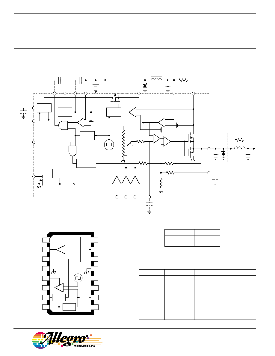
FUNCTIONAL BLOCK DIAGRAM
and typical application
A8281SLB Output Voltage Select Table
VSEL1
V
LNB
L
13 V
H
18 V
A8282SLB Output Voltage Select Table
VSEL0
VSEL1
LLC
V
LNB
L
L
L
13 V
L
L
H
14 V
L
H
L
18 V
L
H
H
19 V
H
L
L
12 V
H
L
H
13 V
H
H
L
20 V
H
H
H
21 V
Copyright © 2003 Allegro MicroSystems, Inc.
A8281SLB
PUMPX
VPUMP
CPUMP
CHARGE
PUMP
15
9
8
1
2
3
4
5
6
7
16
14
13
12
11
10
EXTM
GND
ENT
EN
VSEL1
OLF
VBULK
GND
SENSE
LNB
LX
VIN
TCAP
VOLTAGE
CONTROL
REG.
BUCK
Dwg. PP-072-3
8281
AND
8282
LNB SUPPLY AND
CONTROL-VOLTAGE REGULATORS
www.allegromicro.com
3
ELECTRICAL CHARACTERISTICS: unless otherwise noted at T
J
< 125∞C, C
LNB
= 0.1
µF,
4.5
-
V + V
LNB
< V
IN
< 47
-
V
Characteristic
Symbol
Test Conditions
Limits
Min.
Typ.
Max. Units
Supply Voltage Range
V
IN
Operating
4.5 +V
LNB
--
47
V
Output Voltage Error
(reference Output Voltage
Select table)
E
VLNB
6 mA I
LNB
750 mA, ENT = L
--
0
±4.5
%
12 mA I
LNB
750 mA, ENT = H,
average V
LNB
--
0
±4.5
%
Output Reverse Current
I
RLNB
EN = L, V
LNB
= 22 V, V
IN
= 22 V or fl oating
--
1
5
mA
Buck Switch On Resist.
r
DS(on)
T
J
= 25∞C, I
LNB
= 750 mA
--
0.57
0.67
T
J
= 125∞C, I
LNB
= 750 mA
--
0.84
0.94
Buck Switch Current Limit
I
BSM
1
--
2.5
A
Switching Frequency
f
O
16 x f
tone
320
352
384
kHz
Linear Reg. Volt. Drop
V
BUCK
V
SENSE
≠ V
LNB
, ENT = L, I
LNB
= 750 mA
700
900
1100
mV
Logic Input Voltage
V
IL
--
--
0.8
V
V
IH
2
--
--
V
Logic Input Current
I
IH
V
IH
= 5 V
--
<1.0
10
µA
Supply Current
I
IN
Outputs disabled (EN = L)
--
0.25
1
mA
EN = H, I
LNB
= 0
--
6
10
mA
Tone Characteristics
Tone Frequency
f
tone
ENT = H
20
22
24
kHz
Tone Amplitude
V
tone(PP)(ENT)
ENT = H, 12 mA I
LNB
750 mA
400
650
900
mV
Tone Duty Cycle
dc
tone
ENT = H, 12 mA I
LNB
750 mA
40
--
60
%
Tone Rise or Fall Time
t
r
, t
f
ENT = H, 12 mA I
LNB
750mA
5
10
15
µs
External Modulation
Tone Amplitude
V
tone(PP)(EXTM)
f = 22 kHz square wave, I
LOAD
= 12 mA to
450 mA, V
IN
= 100mV to 125 mV;
V
PP
ac coupled
400
550
800
mV
External Modulation Input
Voltage Range
V
EXTM(PP)
AC coupled
100
--
125
mV
External Modulation Input
Impedance
Z
EXTM
f = 22 kHz
4
--
10
k
continued next page
NOTES: 1. Typical data is for design information only.
2. Negative current is defi ned as coming out of (sourcing) the specifi ed device terminal.

8281
AND
8282
LNB SUPPLY AND
CONTROL-VOLTAGE REGULATORS
115 Northeast Cutoff, Box 15036
Worcester, Massachusetts 01615-0036 (508) 853-5000
4
ELECTRICAL CHARACTERISTICS: unless otherwise noted at T
J
125
∞
C, C
LNB
= 0.1
-
µ
F,
4.5
-
V + V
LNB
V
IN
47
-
V.
Limits
Characteristic
Symbol
Test Conditions
Min.
Typ.
Max.
Units
Protection Circuitry
Current-Limiting Threshold
V
ILNB(th)
V
BULK
≠ V
SENSE
115
135
155
mV
Overload Flag Output Low
V
OLF
I
OLF
= 8
-
mA
--
0.28
0.5
V
Overload Flag Leakage Current
I
OLF
V
OLF
= 5.5
-
V
--
<1.0
10
µ
A
Thermal Shutdown Temp.
T
J
--
165
--
∞
C
Thermal Shutdown Hysteresis
T
J
--
20
--
∞
C
NOTES: 1. Typical data is for design information only.
2. Negative current is defined as coming out of (sourcing) the specified device terminal.

8281
AND
8282
LNB SUPPLY AND
CONTROL-VOLTAGE REGULATORS
5
www.allegromicro.com
Buck regulator.
A current-mode buck converter
provides the linear regulator a supply voltage that
tracks the selected LNB output voltage. The buck
converter operates at 16 times the internal tone fre-
quency, nominally 352
-
kHz.
The tracking regulator provides minimum power
dissipation across the range of output voltages by
adjusting the SENSE terminal voltage, nominally
900
-
mV above the LNB output voltage. The tracking
regulator also provides adequate headroom for tone
injection.
Linear regulator.
The output linear regulator will
sink or source current. This allows tone modulation
into a capacitive load of 0.1
-
µ
F over the output
current range of 12
-
mA to 750
-
mA.
Slew rate control.
The programmed output volt-
age rise and fall times can be set by an external
capacitor (with an internal 25
-
k
resistor) located on
the TCAP terminal. The range of acceptable capaci-
tor values is 4.7
-
nF to 47
-
nF. This feature only
affects the turn-on and programmed voltage rise and
fall times. Modulation is unaffected by the capacitor.
If LNB output voltage rise and fall time limiting is
not required, the TCAP terminal should use a 100
-
nF
ceramic as a default value to minimize output noise.
If a small value capacitor is used, the rise time will be
limited by the time required to charge the VBULK
capacitor.
Short-circuit limit regulator.
The LNB output is
current limited. The short-circuit protection threshold
is set by the value of an external resistor, R
S
, in
conjunction with an internal 135
-
mV reference
voltage (V
ILNB(th)
).
R
S
= 0.135/I
LNBM
where I
LNBM
is the desired current-limit value. The
sense resistor should be chosen based on the maxi-
mum dc plus ac (tone) load current required, internal
V
ILNB(th)
tolerance, and sense resistor accuracy. For
750
-
mA applications, a precision 140
-
m
resistor is
recommended. For 500
-
mA applications, the resistor
value can be raised to 200
-
m
.
In operation, the short-circuit protection produces
current limiting at the input due to the tracking con-
verter. If the output is shorted, the linear regulator
will limit the output current to I
LNBM
.
Fault output.
Short-circuit or thermal shutdown
will cause the OLF terminal, an open-drain diagnostic
output flag, to go LOW.
Internal tone modulation.
The ENT (tone enable)
terminal activates the internal tone signal, modulating
the dc output with a 650
-
mV peak-to-peak trapezoidal
waveform. The internal oscillator is factory trimmed
to provide a tone of 22
-
kHz. No further adjustment is
required. Burst coding of the tone can be accom-
plished, due to the fast response of the ENT input and
rapid tone response. This allows implementation of
the DiSEqCTM protocols.
External tone modulation.
To improve design
flexibility and to allow implementation of proposed
LNB remote control standards, an analog modulation
input terminal is available (EXTM). An appropriate
dc-blocking capacitor must be used to couple the
modulating signal source to the EXTM terminal. The
peak-to-peak input amplitude should stay within
100
-
mV to 125
-
mV to ensure the DiSEqC amplitude
specification over the output current range. If exter-
nal modulation is not used, the EXTM terminal
should be decoupled to ground with a 0.1
-
µ
F ceramic
capacitor.
FUNCTIONAL DESCRIPTION