 | –≠–ª–µ–∫—Ç—Ä–æ–Ω–Ω—ã–π –∫–æ–º–ø–æ–Ω–µ–Ω—Ç: A1392 | –°–∫–∞—á–∞—Ç—å:  PDF PDF  ZIP ZIP |

A1391-DS
A1391 and A1392
Worcester, Massachusetts 01615-0036 (508) 853-5000
115 Northeast Cutoff, Box 15036
www.allegromicro.com
Allegro MicroSystems, Inc.
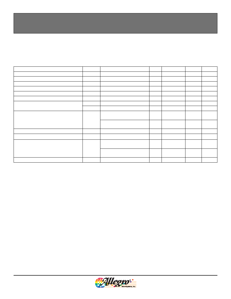
AB SO LUTE MAX I MUM RAT INGS
*
Supply Voltage, V
CC
.............................................8 V
Reverse-Supply Voltage, V
RCC
....................... ≠0.1 V
Ratiometric Supply Reference Voltage, V
REF
...... 7 V
Reverse-Ratiometric Supply
Reference Voltage, V
RREF
.........................≠0.1 V
Logic Supply Voltage, V
Ø
SØ ØLØ ØEØ ØEØ ØPØ
(V
CC
> 2.5 V)...............................................32 V
Reverse-Logic Supply Voltage, V
RØSØ ØLØ ØEØ ØEØ ØPØ
.........≠0.1 V
Output Voltage, V
OUT
............................ V
CC
+ 0.1 V
Reverse-Output Voltage, V
ROUT
...................... ≠0.1 V
Temperatures
Operating
Ambient,
T
A
, Range S.... ≠20∫C to 85∫C
Junction,
T
J(MAX)
.......................................165∫C
Storage,
T
S
................................. ≠65∫C to 170∫C
*All ratings with reference to ground.
Micro Power 3 V Linear Hall Effect Sensor with Tri-State Output
and User-Selectable Sleep Mode
Use the following complete part numbers when ordering:
Package EH, 6-pin MLP/DFN
Features and Benefits
These linear Hall effect sensor integrated circuits (ICs) provide a voltage output that is
directly proportional to an applied magnetic field. Before amplification, the sensitivity of
typical Hall effect ICs (measured in mV/G) is directly proportional to the current flowing
through the Hall effect transducer element inside the ICs. In many applications, it is difficult
to achieve sufficient sensitivity levels with a Hall effect sensor IC without consuming more
than 3 mA of current. The A1391 and A1392 minimize current consumption to less than
25 A through the addition of a user-selectable sleep mode. This makes these devices per-
fect for battery-operated applications such as: cellular phones, digital cameras, and portable
tools. End users can control the current consumption of the A1391 and A1392 by applying
a logic level signal to the ØSØ ØLØ ØEØ ØEØ ØPØ pin. The outputs of the devices are not valid (high-imped-
ance mode) during sleep mode. The high-impedance output feature allows the connection of
multiple A1391 and A1392 Hall effect devices to a single A-to-D converter input.
The quiescent output voltage of these devices is 50 % nominal of the ratiometric supply
reference voltage applied to the VREF pin of the device. The output voltage of the device is
not ratiometric with respect to the SUPPLY pin.
Despite the low power consumption of the circuitry in the A1391 and A1392, the features
required to produce a highly-accurate linear Hall effect IC have not been compromised.
Each BiCMOS monolithic circuit integrates a Hall element, improved temperature-com-
pensating circuitry to reduce the intrinsic sensitivity drift of the Hall element, a small-signal
high-gain amplifier, and proprietary dynamic offset cancellation circuits. End of line, post-
packaging, factory programming allows precise control of device sensitivity and offset.
This device is available in a small 2.0 ◊ 3.0 mm, 0.75 mm nominal height micro leaded pack-
age (MLP). It is Pb (lead) free, with 100 % matte tin leadframe plating.
Part Number
Sensitivity
(mV / G, Typ.)
Packing*
A1391SEHLT-T
1.25
7-in. reel, 3000 pieces/reel
A1392SEHLT-T
2.50
7-in. reel, 3000 pieces/reel
*Contact Allegro for additional packing options.
∑ High-impedance output during sleep mode
∑ Compatible with 2.5 to 3.5 V power supplies
∑ 10 mW power consumption in the active mode
∑ Miniature MLP package
∑ Ratiometric output scales with the ratiometric supply reference voltage (VREF pin)
∑ Temperature-stable quiescent output voltage and sensitivity
∑ Wide ambient temperature range: ≠20∞C to 85∞C
∑ ESD protection greater than 3 kV
∑ Solid-state reliability
∑ Preset sensitivity and offset at final test
6
5
1
2
3
4
VCC
OUT
GND
VREF
GND
SLEEP

A1391-DS
2
Worcester, Massachusetts 01615-0036 (508) 853-5000
115 Northeast Cutoff, Box 15036
www.allegromicro.com
Allegro MicroSystems, Inc.
Micro Power 3 V Linear Hall Effect Sensor with Tri-State Output and User-Selectable Sleep Mode
A1391 and A1392
Functional Block Diagram
Amp
Out
VCC
OUT
GND
Filter
Dynamic Of
fset
Cancellation
Gain
Offset
Hall Element
Regulator
Programming Logic
Circuit Reference Current
To all subcircuits
R
Ratio
/ 2
R
Ratio
/ 2
VREF
SLEEP
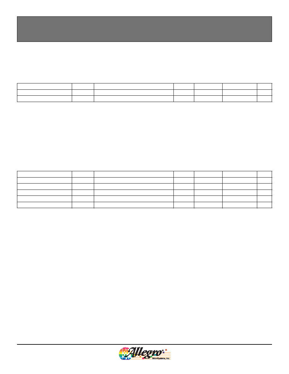
Terminal List Table
Pin
Name
Function
1
VCC
Supply
2
OUT
Output
3
GND
Ground
4
GND
Ground
5
ØSØ ØLØ ØEØ ØEØ ØPØ
Toggle sleep mode
6
VREF
Supply for ratiometric reference
A1391-DS
3
Worcester, Massachusetts 01615-0036 (508) 853-5000
115 Northeast Cutoff, Box 15036
www.allegromicro.com
Allegro MicroSystems, Inc.
Micro Power 3 V Linear Hall Effect Sensor with Tri-State Output and User-Selectable Sleep Mode
A1391 and A1392
Device Characteristics Tables
ELECTRICAL CHARACTERISTICS valid through full operating ambient temperature range, unless otherwise noted
Characteristic
Symbol
Test Conditions
Min.
Typ.
1
Max.
Units
Supply Voltage
V
CC
2.5
≠
3.5
V
Nominal Supply Voltage
V
CCN
≠
3.0
≠
V
Supply Zener Clamp Voltage
V
CCZ
I
CC
= 7 mA, T
A
= 25∞C
6
8.3
≠
V
Ratiometric Reference Voltage
2
V
REF
2.5
≠
V
CC
V
Ratiometric Reference Zener Clamp Voltage
V
REFZ
I
VREF
=
3 mA, T
A
= 25∞C
6
8.3
≠
V
ØSØ ØLØ ØEØ ØEØ ØPØ Input Voltage
≠0.1
≠
V
CC
+ 0.5
V
ØSØ ØLØ ØEØ ØEØ ØPØ Input Threshold
V
INH
For active mode
≠
0.45 ◊ V
CC
≠
V
V
INL
For sleep mode
≠
0.20 ◊ V
CC
≠
V
Ratiometric Reference Input Resistance
R
REF
V
SLEEP
> V
INH
, V
CC
=
V
CCN,
T
A
= 25∞C
250
≠
≠
k
V
SLEEP
< V
INL,
V
CC
=
V
CCN,
T
A
= 25∞C
≠
5
≠
M
Chopper Stabilization Chopping Frequency
f
C
V
CC
=
V
CCN
, T
A
= 25∞C
≠
200
≠
kHz
ØSØ ØLØ ØEØ ØEØ ØPØ Input Current
I
SLEEP
V
SLEEP
= 3 V, V
CC
= V
CCN
≠
1
≠
A
Supply Current
3
I
CC
V
SLEEP
< V
INL,
V
CC
=
V
CCN,
T
A
= 25∞C
≠
0.025
≠
mA
V
SLEEP
> V
INH
, V
CC
=
V
CCN,
T
A
= 25∞C
≠
3.2
≠
mA
Quiescent Output Power Supply Rejection
4
PSR
VOQ
f
AC
< 1 kHz
≠
≠60
≠
dB
1
Typical data are for initial design estimations only, and assume optimum manufacturing and application conditions, such as T
A
= 25∞C. Performance
may vary for individual units, within the specified maximum and minimum limits.
2
Voltage applied to the VREF pin. Note that the V
REF
voltage must be less than or equal to V
cc
. Degradation in device accuracy will occur with applied
voltages of less than 2.5 V.
3
If the VREF pin is tied to the VCC pin, the supply current would be I
CC
+ V
REF
/ R
REF
4
f
AC
is any ac component frequency that exists on the supply line.

A1391-DS
4
Worcester, Massachusetts 01615-0036 (508) 853-5000
115 Northeast Cutoff, Box 15036
www.allegromicro.com
Allegro MicroSystems, Inc.
Micro Power 3 V Linear Hall Effect Sensor with Tri-State Output and User-Selectable Sleep Mode
A1391 and A1392
OUTPUT CHARACTERISTICS valid through full operating ambient temperature range, unless otherwise noted
Characteristic
Symbol
Test Conditions
Min.
Typ.
1
Max.
Units
Output Voltage Saturation
Limits
2
V
OUTH
B =
X
, V
CC
= V
CCN
, V
REF
V
CC
≠
V
REF
≠ 0.1
≠
V
V
OUTL
B = ≠
X
, V
CC
= V
CCN
, V
REF
V
CC
≠
0.1
≠
V
Maximum Voltage Applied
to Output
V
OUTMAX
V
SLEEP
< V
INL
≠
≠
V
CC
+ 0.1
V
Sensitivity
3
Sens
A1391 T
A
= 25∞C, V
CC
= V
REF
= V
CCN
1.18
1.25
1.31
mV/G
A1392 T
A
= 25∞C, V
CC
= V
REF
= V
CCN
2.35
2.50
2.65
mV/G
Quiescent Output
V
OUTQ
T
A
= 25∞C, B = 0 G
≠
0.500 ◊ V
REF
(0.500 ◊ V
REF
)
± 0.030
V
Output Resistance
4
R
OUT
f
out
= 1 kHz, V
SLEEP
> V
INH
, active mode
≠
20
≠
f
out
= 1 kHz, V
SLEEP
< V
INL
, sleep mode
≠
4M
≠
Output Load Resistance
R
L
Output to ground
15
≠
≠
k
Output Load Capacitance
C
L
Output to ground
≠
≠
10
nF
Output Bandwidth
BW
≠3 dB point, V
OUT
= 1 V
pp
sinusoidal,
V
CC
= V
CCN
≠
10
≠
kHz
Noise
5,6
V
n
1391
C
bypass
= 0.1 F,
BW
externalLPF
= 2 kHz
≠
6
12
mV
pp
C
bypass
= 0.1 F, no load
≠
≠
20
mV
pp
1392
C
bypass
= 0.1 F, no load
≠
≠
40
mV
pp
1
Typical data are for initial design estimations only, and assume optimum manufacturing and application conditions, such as T
A
= 25∞C. Performance
may vary for individual units, within the specified maximum and minimum limits.
2
This test requires positive and negative magnetic fields sufficient to swing the output driver between fully OFF and saturated (ON), respectively. The
value of vector
X
is NOT intended to indicate a range of linear operation.
3
For V
REF
values other than V
REF
= V
CCN
, the sensitivity can be derived from the following equation: 0.416 ◊ V
REF
.
4
f
OUT
is the output signal frequency
5
Noise specification includes digital and analog noise.
5
Values for
BW
externalLPF
do not include any noise resulting from noise on the externally-supplied VREF voltage.
A1391-DS
5
Worcester, Massachusetts 01615-0036 (508) 853-5000
115 Northeast Cutoff, Box 15036
www.allegromicro.com
Allegro MicroSystems, Inc.
Micro Power 3 V Linear Hall Effect Sensor with Tri-State Output and User-Selectable Sleep Mode
A1391 and A1392
OUTPUT TIMING CHARACTERISTICS
1
T
A
= 25∞C
Characteristic
Symbol
Test Conditions
Min.
Typ.
2
Max.
Units
Power-On Time
3
t
PON
≠
40
60
s
Power-Off Time
4
t
POFF
≠
1
≠
s
1
See figure 1 for explicit timing delays.
2
Typical data are for initial design estimations only, and assume optimum manufacturing and application conditions, such as T
A
= 25∞C. Performance
may vary for individual units, within the specified maximum and minimum limits.
3
Power-On Time is the elapsed time after the voltage on the SLEEP pin exceeds the active mode threshold voltage,V
INH
, until the time the device output
reaches 90% of its value. When the device output is loaded with the maximum capacitance of 10 nF, the Power-On Time range is guaranteed for input
SLEEP pin frequencies less than 10 Hz.
4
Power-Off Time is the duration of time between when the signal on the SLEEP pin switches from HIGH to LOW and when I
CC
drops to under 100 A.
During this time period, the output goes into the HIGH impedance state.
MAGNETIC CHARACTERISTICS
T
A
= 25∞C
Characteristic
Symbol
Test Conditions
Min.
Typ.*
Max.
Units
Ratiometry
V
OUTQ(
V)
≠
100
≠
%
Ratiometry
Sens
(
V)
≠
100
≠
%
Positive Linearity
Lin+
≠
100
≠
%
Negative Linearity
Lin ≠
≠
100
≠
%
Symmetry
Sym
≠
100
≠
%
*Typical data are for initial design estimations only, and assume optimum manufacturing and application conditions, such as T
A
= 25∞C. Performance
may vary for individual units, within the specified maximum and minimum limits.