 | –≠–ª–µ–∫—Ç—Ä–æ–Ω–Ω—ã–π –∫–æ–º–ø–æ–Ω–µ–Ω—Ç: A2540SLB | –°–∫–∞—á–∞—Ç—å:  PDF PDF  ZIP ZIP |

QUAD DARLINGTON
POWER DRIVER
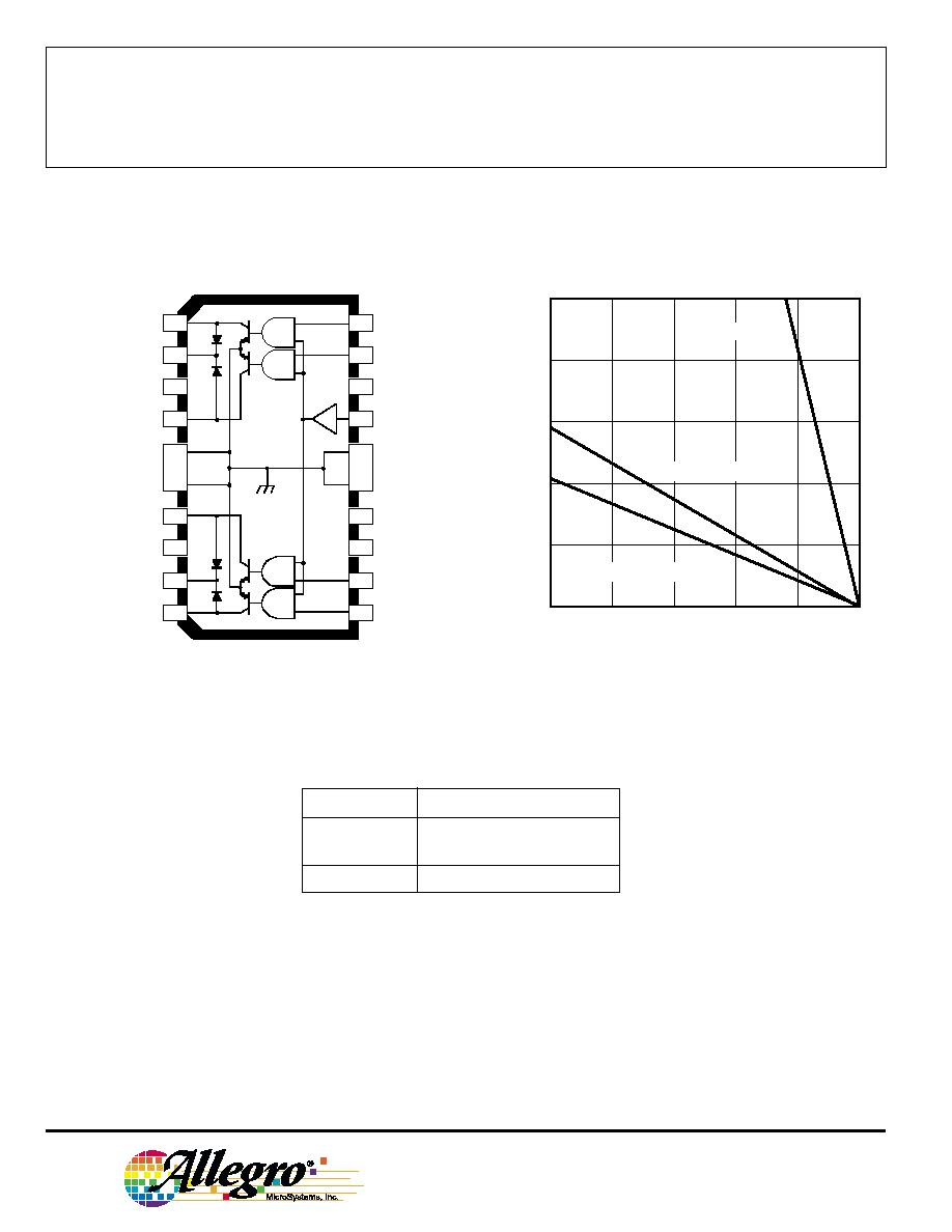
Combining AND logic gates and inverting high-current bipolar
outputs, the UDN2540B and A2540SLB quad Darlington power drivers
provide interface between low-level signal-processing circuits and
power loads totaling 360 W. Each of the four independent outputs can
sink up to 1.8 A in the on state with peak inrush currents to 2.5 A. The
four power outputs are each comprised of an open-collector Darlington
driver and an internal flyback/clamp diode for switching inductive
leads. They feature a minimum breakdown and sustaining voltage of
50 V. The logic inputs are compatible with TTL and 5 V CMOS logic
systems.
Typical applications include print heads, relays, solenoids, and
dc stepping motors. These drivers can also be used to drive high-
current incandescent lamps, LEDS, and heaters. A similar device,
specifically intended for driving a unipolar stepper motor in the
two-phase drive format, is the UDN2544B.
The UDN2540B is supplied in a 16-pin batwing power DIP; the
A2540SLB is supplied in a 20-lead batwing power SOIC for surface-
mount applications. The batwing construction provides for maximum
package power dissipation in a standard construction. At 25
∞C, and
with only 1 sq. in. of copper foil at the ground tabs, either package is
capable of safely dissipating more than 2 W.
FEATURES
I 1.8 A Continuous Output Current
I Output Voltage to 50 V
I TTL and 5 V CMOS Compatible Inputs
I Efficient Input/Output Pinning
I Integral Transient-Suppression Diodes
I Replaces L6221A and L6221CD
Data Sheet
29317C
UDN2540B
ABSOLUTE MAXIMUM RATINGS
at T
A
= 25
∞C
Output Voltage, V
OUT
........................... 50 V
Output Current, I
OUT
(peak) ................ 2.5 A
(continuous) .................................. 1.8 A
Logic Supply Voltage, V
CC
.................. 7.0 V
Input Voltage, V
IN
................................ 7.0 V
Package Power Dissipation,
P
D
........................................ See Graph
Operating Temperature Range,
T
A
.................................. -20
∞
C to +85
∞
C
Storage Temperature Range,
T
S
................................ -55
∞
C to +150
∞
C
1
2
3
14
4
5
6
7
8
9
10
11
12
13
15
16
ENABLE
GROUND
GROUND
OUT
2
K
GROUND
GROUND
OUT
3
OUT
4
K
OUT
1
V
CC
IN
1
Dwg. PP-017-2
IN
4
IN
3
IN
2
Always order by complete part number:
Part Number
Package
UDN2540B
16-pin batwing DIP
A2540SLB
20-lead batwing SOIC
2540
115 Northeast Cutoff, Box 15036
Worcester, Massachusetts 01615-0036 (508) 853-5000
2540
QUAD DARLINGTON
POWER DRIVER
TRUTH TABLE
ENABLE
IN
N
OUT
N
H
H
ON
--
L
OFF
L
X
OFF
X = Don't care.
ENABLE
GROUND
GROUND
OUT
2
K
GROUND
GROUND
OUT
3
OUT
4
K
OUT
1
V
CC
IN
1
IN
2
IN
4
IN
3
13
14
17
19
12
18
20
11
NO
CONNECTION
NO
CONNECTION
NC
NC
1
2
3
9
4
7
10
5
6
8
Dwg. PP-017-3
NO
CONNECTION
NO
CONNECTION
NC
NC
SUPPLY
16
15
A2540SLB
50
75
100
125
150
5
1
0
ALLOWABLE PACKAGE POWER DISSIPATION IN WATTS
TEMPERATURE IN
∞C
4
3
2
25
Dwg. GP-049-3
R = 6.0
∞C/W
JT
SUFFIX 'B', R = 43
∞C/W
JA
SUFFIX 'LB', R = 60
∞C/W
JA
Copyright © 1986, 1996 Allegro MicroSystems, Inc.

2540
QUAD DARLINGTON
POWER DRIVER
www.allegromicro.com
Limits
Characteristic
Symbol
Test Conditions
Min.
Typ.
Max.
Units
Output Leakage Current
I
CEX
V
OUT
= 50 V, V
IN
= 0.8 V, V
EN
= 2.4 V
--
<1.0
100
µA
V
OUT
= 50 V, V
IN
= 2.4 V, V
EN
= 0.8 V
--
<1.0
100
µA
Output Sustaining Voltage
V
CE(sus)
I
OUT
= 1.8 A, L = 3.0 mH
50
--
--
V
Output Saturation Voltage
V
CE(SAT)
I
OUT
= 600 mA, V
IN
= V
EN
= 2.4 V
--
0.9
1.0
V
I
OUT
= 1.0 A, V
IN
= V
EN
= 2.4 V
--
1.0
1.2
V
I
OUT
= 1.8 A, V
IN
= V
EN
= 2.4 V
--
1.3
1.6
V
Input Voltage
Logic 1
V
IN(1)
or V
EN(1)
2.4
--
--
V
Logic 0
V
lN(0)
or V
EN(0)
--
--
0.8
V
Input Current
Logic 1
V
IN(1)
or V
EN(1)
= 2.4 V
--
--
10
µA
Logic 0
V
lN(0)
or V
EN(0)
= 0.8 V
--
--
-100
µA
Total Supply Current
I
CC
V
IN
* = V
EN
= 2.4 V, V
CC
= 5.0 V,
--
14
20
mA
Outputs Open
V
IN
* = V
EN
= 0.8 V, V
CC
= 5.0 V
--
0.4
2.0
mA
Clamp Diode Forward Voltage
V
F
I
F
= 1.0 A
--
1.3
1.6
V
I
F
= 1.8 A
--
1.6
2.0
V
Clamp Diode Leakage Current
I
R
V
R
= 50 V
--
<1.0
100
µA
Typical Data is for design information only.
Negative current is defined as coming out of (sourcing) the specified terminal.
As used here, -100 is defined as greater than +10 (absolute magnitude convention) and the minimum is implicitly zero.
*All inputs simultaneously, all other tests are performed with each input tested separately.
ELECTRICAL CHARACTERISTICS at T
A
= 25
∞
C, T
J
150
∞
C, V
CC
= 4.75 V to 5.25 V.

115 Northeast Cutoff, Box 15036
Worcester, Massachusetts 01615-0036 (508) 853-5000
2540
QUAD DARLINGTON
POWER DRIVER
APPLICATIONS INFORMATION
A typical application is shown for driving four high-current relays,
solenoids, or print heads. A Zener diode is used to increase the
flyback voltage, providing a much faster inductive load turn-off current
decay, resulting in faster dropout (reduced relay contact arcing), and
improved performance. The maximum Zener voltage, plus the load
supply voltage, plus the flyback diode forward voltage must not exceed
the device's rated sustaining voltage.
With external control circuitry, the ENABLE input can be used for
chopper (PWM) applications. If the ENABLE input is not used, it
should be tied high.
All inputs will float high if open circuited.
Dwg. WP-001
TYPICAL APPLICATION
(QUAD RELAY DRIVER WITH ZENER FLYBACK)
Dwg. EP-016
+5V
4
IN
ENABLE
IN
3
IN
IN
1
2
+28 V
K
K
4
3
K
2
15V
K
1
1
2
3
4
5
6
7
8
16
15
14
13
12
11
10
9
OUTPUT
VOLTAGE
OUTPUT
CURRENT
ZENER CLAMP
DIODE CLAMP
V
CC
V
CE(SAT)
I
OUT
I
CEX
V + V
CC
F
V + V + V
CC
Z
F
2540
QUAD DARLINGTON
POWER DRIVER
www.allegromicro.com
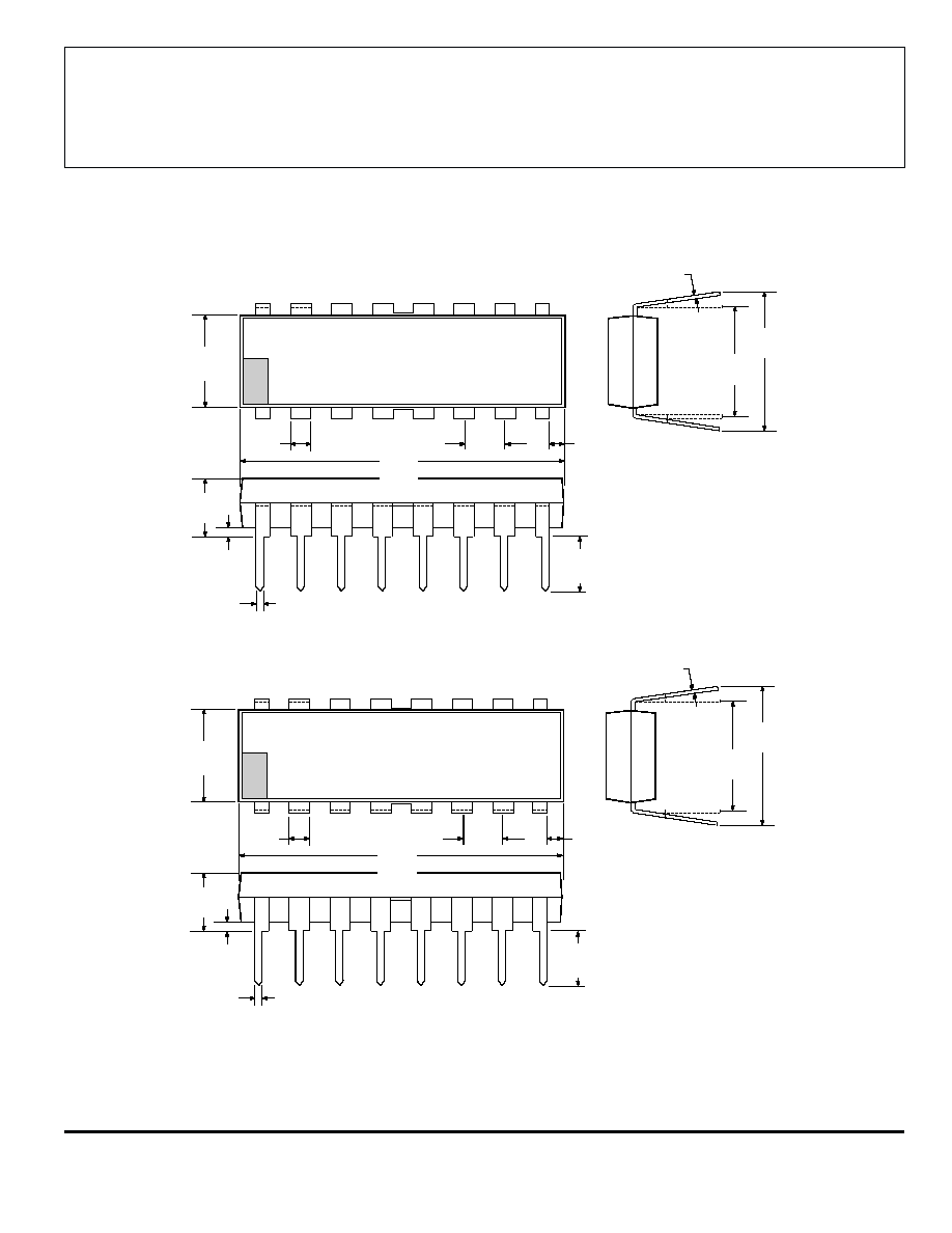
NOTES: 1. Leads 1, 8, 9, and 16 may be half leads at vendor's option.
2. Lead thickness is measured at seating plane or below.
3. Lead spacing tolerance is non-cumulative.
4. Webbed lead frame. Leads indicated are internally one piece.
5. Exact body and lead configuration at vendor's option within limits shown.
Dimensions in Millimeters
(for reference only)
0.020
0.008
0.300
BSC
Dwg. MA-001-17A in
0.430
MAX
16
1
8
0.280
0.240
0.210
MAX
0.070
0.045
0.015
MIN
0.022
0.014
0.100
BSC
0.005
MIN
0.150
0.115
9
0.775
0.735
NOTE 4
UDN2540B
Dimensions in Inches
(controlling dimensions)
0.508
0.204
7.62
BSC
Dwg. MA-001-17A mm
10.92
MAX
16
1
8
7.11
6.10
5.33
MAX
1.77
1.15
0.39
MIN
0.558
0.356
2.54
BSC
0.13
MIN
3.81
2.93
9
19.68
18.67
NOTE 4