
NOTE: For detailed information on purchasing options, contact your
local Allegro field applications engineer or sales representative.
Allegro MicroSystems, Inc. reserves the right to make, from time to time, revisions to the anticipated product life cycle plan for a
product to accommodate changes in production capabilities, alternative product availabilities, or market demand. The information
included herein is believed to be accurate and reliable. However, Allegro MicroSystems, Inc. assumes no responsibility for its use; nor
for any infringements of patents or other rights of third parties which may result from its use.
Recommended Substitutions:
Protected Quad Driver
A2547
Date of status change: May 2, 2005
Deadline for receipt of LAST TIME BUY orders: October 28, 2005
These parts are in production but have been determined to be
LAST TIME BUY. This classification indicates that the product is
obsolete and notice has been given. Sale of this device is currently
restricted to existing customer applications. The device should not be
purchased for new design applications because of obsolescence in the
near future. Samples are no longer available.
Last Time Buy

Providing interface between low-level logic and power loads, the
UDK/UDN/UDQ2547B and UDK/UDN/UDQ2547EB quad power
drivers combine logic gates and high-current bipolar outputs with
complete output protection. Each of the four outputs will sink 600 mA
in the ON state. The outputs have a minimum breakdown voltage
(load dump) of 60 V and a sustaining voltage of 40 V. The inputs are
compatible with TTL and 5 V CMOS logic systems and include internal
pull-down resistors to ensure that the outputs remain OFF if the inputs
are open-circuited.
Over-current protection for each channel has been designed into
these devices and is activated at approximately 1.3 A. It protects each
output from short circuits with supply voltages up to 25 V. When a
maximum driver output current is reached, that output drive is reduced
linearly, maintaining a constant load current. If the over-current or
short circuit condition continues, each channel has an independent
thermal limit circuit which will sense the rise in junction temperature
and turn OFF the individual channel that is at fault. Foldback circuitry
decreases the output current if excessive voltage is present across the
output and assists in keeping the device within its SOA (safe operating
area).
Each output also includes diagnostics for increased device protec-
tion. If any output is shorted or opened, the diagnostics can signal the
controlling circuitry through a common FAULT pin.
These devices can be used to drive various resistive loads includ-
ing incandescent lamps (without warming or limiting resistors). With
the addition of external output clamp diodes, they can be used to drive
inductive loads such as relays, solenoids, or dc stepping motors.
The suffix `B' devices are 16-pin power DIPs while the suffix `EB'
devices are 28-lead power PLCCs for surface-mount applications.
Both packages are of batwing construction to provide for maximum
package power dissipation.
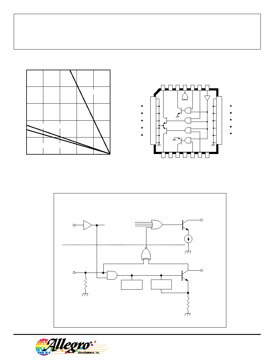
UDx2547B
(DIP)
2547
PROTECTED
QUAD POWER DRIVER
ABSOLUTE MAXIMUM RATINGS
at T
A
= 25
�
C
Output Voltage, V
OUT
............................ 60 V
Over-Current Protected Output Voltage,
V
OUT
............................................... 25 V
Output Current, I
OUT
.......................... 1.3 A*
FAULT Output Voltage, V
F
................... 40 V
Supply Voltage, V
CC
............................ 7.0 V
Input Voltage, V
IN
or V
EN
...................... 7.0 V
Package Power Dissipation,
P
D
........................................ See Graph
Operating Temperature Range, T
A
Prefix `UDK' ............... -40
�
C to +125
�
C
Prefix `UDN' ................. -20
�
C to +85
�
C
Prefix `UDQ' ................. -40
�
C to +85
�
C
Storage Temperature Range,
T
S
............................... -55
�
C to +150
�
C
*Outputs are current limited at approximately
1.3 A per driver and junction temperature limited
if current in excess of 1.3 A is attempted. See
Circuit Description and Application for further
information.
Always order by complete part number: a prefix to indicate operat-
ing temperature range + the basic four-digit part number + a suffix to
indicate package style, e.g., UDK2547EB .
FEATURES
s
Output SOA Protection
s
Low Output-Saturation Voltage
s
Diagnostic FAULT Output
s
TTL and 5 V CMOS Compatible Inputs
s
Independent Over-Current
Protection for Each Driver
s
Independent Thermal Protection for Each Driver
s
600 mA Output Current per Channel
Data Sheet
29317.4C*
1
2
3
14
4
5
6
7
8
9
10
11
12
13
15
16
ENABLE
GROUND
GROUND
OUT
3
NO
CONNECT.
GROUND
GROUND
OUT
2
OUT
1
FAULT
OUT
4
V
CC
IN
4
Dwg. PP-018A
IN
1
IN
2
IN
3
SUPPLY
2547
PROTECTED
QUAD POWER DRIVER
115 Northeast Cutoff, Box 15036
Worcester, Massachusetts 01615-0036 (508) 853-5000
UDx2547EB
(PLCC)
FUNCTIONAL BLOCK DIAGRAM
<<1
OUT
Dwg. FP-007
N
FAULT
COMMON CONTROL
ONE OF FOUR DRIVERS
ABLE
IN N
CURRENT
LIMIT
THERMAL
SHUTDOWN
1
2
3
4
5
6
7
8
9
10
11
12
13
14
15
16
17
18
19
20
21
22
23
24
25
26
27
28
GROUND
GROUND
GROUND
GROUND
Dwg. PP-019
NO
CONNECTION
NC
ENABLE
SUPPLY
NC
CC
V
OUT
1
OUT
2
OUT
3
OUT
4
IN
4
IN
3
IN
2
IN
1
NO
CONNECTION
NO
CONNECTION
FAULT
NC
FAULT
Copyright � 1989, 2002 Allegro MicroSystems, Inc.
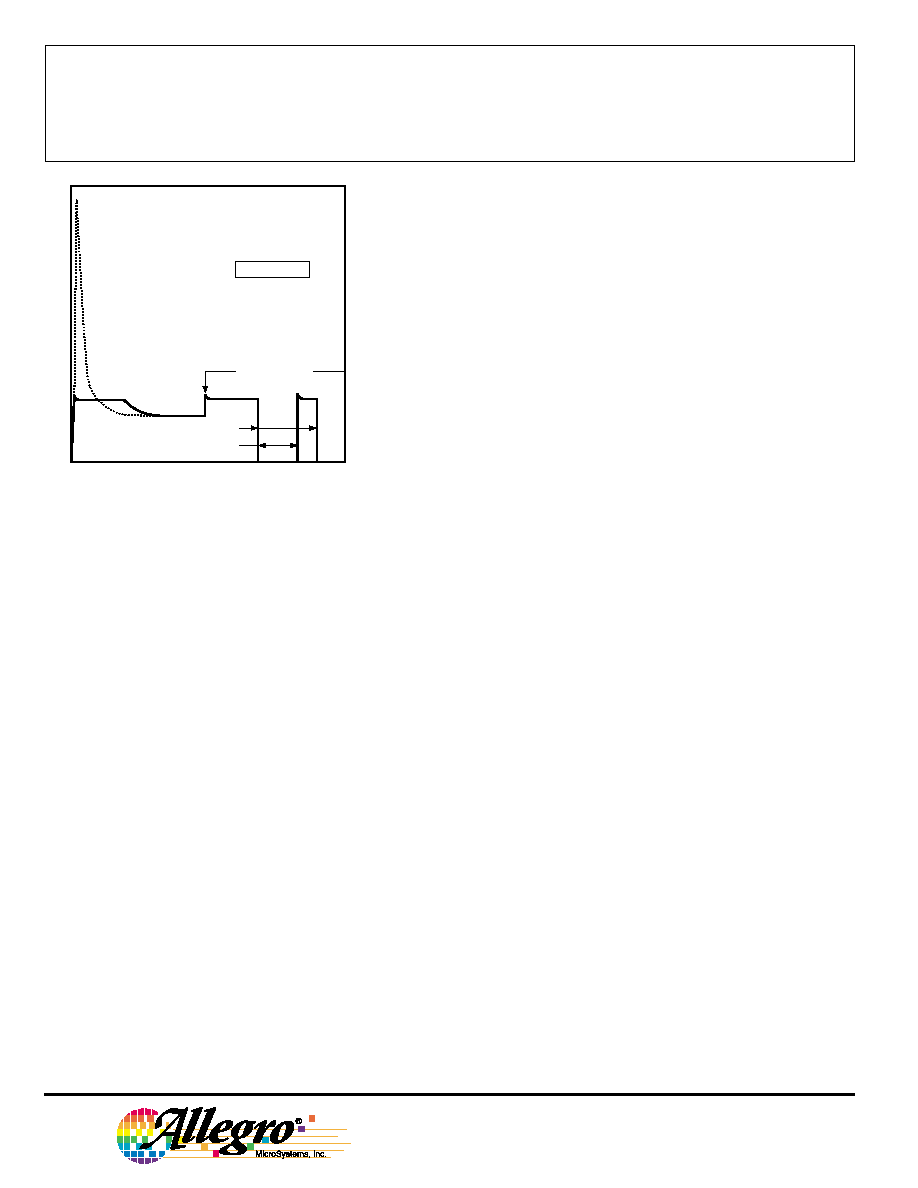
50
75
100
125
150
10
6
4
2
0
ALLOWABLE PACKAGE POWER DISSIPATION IN WATTS
TEMPERATURE IN
�
�
�
�
C
8
25
R = 6
�
C/W
JT
Dwg. GP-004-1A
SUFFIX 'EB', R = 36
�
C/W
JA
SUFFIX 'B', R = 43
�
C/W
JA

2547
PROTECTED
QUAD POWER DRIVER
STATUS
IN
N
ENABLE
OUT
N
FAULT
Normal Load
H
H
L
H
L
H
H
H
X
L
H
H
Over-Current or
Short to Supply
H
H
R
L
Thermal Fault
H
H
H
L
Open Load or
Short to Ground
L
H
L
L
ELECTRICAL CHARACTERISTICS at T
A
= +25
�
C (prefix `UDN') or over operating
temperature range (prefix `UDK' or `UDQ'), V
CC
= 4.75 V to 5.5 V
Limits
Characteristic
Symbol
Test Conditions
Min.
Typ.
Max.
Units
Output Leakage Current*
I
OUT
V
OUT
= 60 V, V
IN
= 0.8 V, V
EN
= 2.0 V
--
30
150
�
A
V
OUT
= 60 V, V
IN
= 2.0 V, V
EN
= 0.8 V
--
30
150
�
A
Output Sustaining Voltage
V
OUT(SUS)
I
OUT
= 100 mA, V
IN
= 0.8 V, V
CC
= Open
40
--
--
V
Output Saturation Voltage
V
OUT(SAT)
I
OUT
= 400 mA
--
--
300
mV
I
OUT
= 500 mA
--
--
400
mV
I
OUT
= 600 mA
--
--
550
mV
Over-Current Limit
I
OUT
5 ms PulseTest, V
OUT
= 5.0 V
--
1. 3
1.7
A
Input Voltage
Logic 1
V
IN(1)
or V
EN(1)
2.0
--
--
V
Logic 0
V
lN(0)
or V
EN(0)
--
--
0.8
V
Input Current
Logic 1
V
IN(1)
or V
EN(1)
= 2.0 V
--
--
60
�
A
Logic 0
V
IN(0)
or V
EN(0)
= 0.8 V
10
--
--
�
A
Fault Output Leakage Current
I
F
V
F
= 40 V
--
<1.0
2.0
�
A
Fault Output Current
I
F
V
F
=
40 V, Driver Outputs Open,
V
IN
= 0.8 V, V
EN
= 2.0 V
40
60
80
�
A
Fault Output Saturation Voltage
V
F(SAT)
I
F
= 30
�
A
--
0.1
0.4
V
Total Supply Current
I
CC
All Outputs ON
--
45
50
mA
All Outputs OFF
--
6.0
10
mA
Thermal Shutdown
T
J
--
165
--
�
C
Thermal Hysteresis
T
J
--
15
--
�
C
Typical Data is for design information only.
*Measurement includes XOR input current
and other elements.
X = Don't care.
R = Linear drive, current limited.
TRUTH TABLE
2547
PROTECTED
QUAD POWER DRIVER
115 Northeast Cutoff, Box 15036
Worcester, Massachusetts 01615-0036 (508) 853-5000
CIRCUIT DESCRIPTION AND APPLICATION
These devices monitor their outputs for open or shorted conditions.
Both conditions are sensed by comparing the input and output states.
Note that the FAULT output is operational only if the ENABLE input is
high. When a fault condition is sensed, the FAULT output will go to a
low state. An external FAULT output filter capacitor (0.1
�
F) is recom-
mended to eliminate erroneous switching.
INCANDESCENT LAMP DRIVER
High incandescent lamp turn-ON/in-rush currents can contribute to
poor lamp reliability and destroy semiconductor lamp drivers.
Warming (parallel) or current-limiting (series) resistors protect both
driver and lamp but use significant power either when the lamp is OFF
or when the lamp is ON, respectively. Lamps with steady-state current
ratings up to 600 mA can be driven without the need for warming or
current-limiting resistors, if lamp turn-ON time is not a concern.
When an incandescent lamp is initially turned ON, the cold filament
is at minimum resistance and would normally allow a 10x to 12x in-rush
current. With these drivers, during turn-ON, the high in-rush current is
sensed by the internal low-value sense resistor, drive current to the
output stage is diverted by the shunting transistor, the output stage
operates in a linear mode, and the load current is limited to approxi-
mately 1.3 A. During lamp warmup, the filament resistance increases
to its maximum value, the output driver goes into saturation and applies
maximum rated voltage to the lamp.
INDUCTIVE LOAD DRIVER
With the addition of external clamp diodes, bifilar (unipolar)
stepper motors and other inductive loads can be driven directly.
The external diodes prevent damage to the output transistors by
suppressing the high-voltage spikes that occur when turning
OFF an inductive load. For rapid current decay (fast turn-OFF speeds),
the use of Zener diodes will raise the flyback voltage and improve
performance. However, the peak voltage must not exceed the speci-
fied minimum sustaining voltage (V
SUPPLY
+ V
Z
+ V
F
V
OUT(SUS)
).
OVER-CURRENT CONDITIONS
In the event of a shorted load, or stalled motor, the load current
will attempt to increase. As described above, the drive current to the
affected output stage is linearly reduced (limiting the load current to
about 1.3 A), causing the output stage to go linear. As the junction
temperature of the output stage increases, the thermal shutdown circuit
will shut OFF the affected output. If the fault condition is corrected, the
output driver will return to its normal saturated condition.
NORMAL LAMP IN-RUSH CURRENT
TIME
Dwg. WP-005A
NOT TO SCALE
LAMP CURRENT
CURRENT LIMIT
THERMAL SHUTDOWN
THERMAL HYSTERESIS
SHORT CIRCUIT