 | –≠–ª–µ–∫—Ç—Ä–æ–Ω–Ω—ã–π –∫–æ–º–ø–æ–Ω–µ–Ω—Ç: 7C256-35 | –°–∫–∞—á–∞—Ç—å:  PDF PDF  ZIP ZIP |
ALLIANCE
SEMICONDUCTOR
A
8
A
7
High Performance
32K
◊
8
CMOS SRAM
AS7C256
AS7C256L
32K
◊
8 CMOS SRAM (Common I/O)
LOGIC BLOCK DIAGRAM
FEATURES
∑ Organization: 32,768 words
◊
8 bits
∑ High speed
≠ 10/12/15/20/25/35 ns address access time
≠ 3/3/4/5/6/8 ns output enable access time
∑ Low power consumption
≠ Active:
660 mW max (10 ns cycle)
≠ Standby:
11 mW max, CMOS I/O
2.75 mW max, CMOS I/O, L version
≠ Very low DC component in active power
∑ 2.0V data retention (L version)
∑ Equal access and cycle times
∑ Easy memory expansion with CE and OE inputs
∑ TTL-compatible, three-state I/O
∑ 28-pin JEDEC standard packages
≠ 300 mil PDIP and SOJ
Socket compatible with 7C512 and 7C1024
≠ 330 mil SOIC
≠ 8
◊
13.4 TSOP
∑ ESD protection > 2000 volts
∑ Latch-up current > 200 mA
SELECTION GUIDE
PIN ARRANGEMENT
256
◊
128
◊
8
ARRAY
(262,144)
INPUT BUFFER
A0
A1
A2
A3
A4
A5
A6
A14
A
9
A
10
A
11
A
12
A
13
I/O0
I/O7
Vcc
GND
OE
CE
WE
COLUMN DECODER
R
O
W
DE
C
ODE
R
CONTROL
CIRCUIT
1
2
3
4
5
6
7
8
9
10
11
12
13
14
28
27
26
25
24
23
22
21
20
19
18
17
Vcc
WE
A13
A8
A9
A11
OE
A10
CE
I/O7
I/O6
I/O5
I/O4
I/O3
A14
A12
A7
A6
A5
A4
A3
A2
A1
A0
I/O0
I/O1
I/O2
GND
AS
7C25
6
16
15
S
E
NS
E
AM
P
AS7C256-02
AS7C256-01
7C256-10
7C256-12
7C256-15
7C256-20
7C256-25
7C256-35
Unit
Maximum Address Access Time
10
12
15
20
25
35
ns
Maximum Output Enable Access Time
3
3
4
5
6
8
ns
Maximum Operating Current
120
115
110
100
90
80
mA
Maximum CMOS Standby Current
2.0
2.0
2.0
2.0
2.0
2.0
mA
L
0.5
0.5
0.5
0.5
0.5
0.5
mA
Vcc
WE
A13
A8
A9
A11
OE
A10
CE
I/O7
I/O6
I/O5
I/O4
I/O3
A14
A12
A7
A6
A5
A4
A3
A2
A1
A0
I/O0
I/O1
I/O2
GND
DIP, SOJ, SOIC
TSOP 8
◊
13.4
22
23
24
25
26
27
28
1
2
3
4
5
6
7
21
20
19
18
17
16
15
14
13
12
11
10
AS7C256
9
8
AS7C256
AS7C256L
2
The AS7C256 is a high performance CMOS 262,144-bit
Static Random Access Memory (SRAM) organized as
32,768 words
◊
8 bits. It is designed for memory applica-
tions where fast data access, low power, and simple interfac-
ing are desired.
Equal address access and cycle times (t
AA
, t
RC
, t
WC
) of
10/12/15/20/25/35 ns with output enable access times (t
OE
)
of 3/3/4/5/6/8 ns are ideal for high performance applica-
tions. A chip enable (CE) input permits easy memory
expansion with multiple-bank memory organizations.
When CE is HIGH the device enters standby mode. The
standard AS7C256 is guaranteed not to exceed 11 mW
power consumption in standby mode; the L version is guar-
anteed not to exceed 2.75 mW, and typically requires only
500
µ
W. The L version also offers 2.0V data retention, with
maximum power consumption in this mode of 300
µ
W.
A write cycle is accomplished by asserting chip enable (CE)
and write enable (WE) LOW. Data on the input pins
I/O0-I/O7 is written on the rising edge of WE (write cycle 1)
or CE (write cycle 2). To avoid bus contention, external
devices should drive I/O pins only after outputs have been
disabled with output enable (OE) or write enable (WE).
A read cycle is accomplished by asserting chip enable (CE)
and output enable (OE) LOW, with write enable (WE)
HIGH. The chip drives I/O pins with the data word refer-
enced by the input address. When chip enable or output
enable is HIGH, or write enable is LOW, output drivers stay
in high-impedance mode.
All chip inputs and outputs are TTL-compatible, and opera-
tion is from a single 5V supply. The AS7C256 is packaged
in all high volume industry standard packages.
FUNCTIONAL DESCRIPTION
.
Parameter
Symbol
Min
Max
Unit
Voltage on Any Pin Relative to GND
V
t
≠0.5
+7.0
V
Power Dissipation
P
D
≠
1.0
W
Storage Temperature (Plastic)
T
stg
≠55
+150
o
C
Temperature Under Bias
T
bias
≠10 +85
o
C
DC Output Current
I
out
≠
20
mA
NOTE: Stresses greater than those listed under Absolute Maximum Ratings may cause permanent damage to the device. This is a stress
rating only and functional operation of the device at these or any other conditions outside those indicated in the operational sections of
this specification is not implied. Exposure to absolute maximum rating conditions for extended periods may affect reliability.
CE
WE
OE
Data
Mode
H
X
X
High Z
Standby (I
SB
, I
SB1
)
L
H
H
High Z
Output Disable
L
H
L
D
out
Read
L
L
X
D
in
Write
Key: X = Don't Care, L = LOW, H = HIGH
ABSOLUTE MAXIMUM RATINGS
TRUTH TABLE
AS7C256
AS7C256L
3
Parameter
Symbol
Min
Typ
Max
Unit
Supply Voltage
V
CC
4.5
5.0
5.5
V
GND
0.0
0.0
0.0
V
Input Voltage
V
IH
2.2
≠
V
CC
+1
V
V
IL
≠0.5*
≠
0.8
V
*V
IL
min = ≠3.0V for pulse width less than t
RC
/2.
Parameter
Symbol Test Conditions
-10
-12
-15
-20
-25
-35
Unit
Min Max Min Max Min Max Min Max Min Max Min Max
Input Leakage
Current
|
I
LI
|
V
CC
= Max,
V
in
= GND to V
CC
≠
1
≠
1
≠
1
≠
1
≠
1
≠
1
µ
A
Output Leakage
Current
|
I
LO
|
CE = V
IH
, V
CC
= Max,
V
out
= GND to V
CC
≠
1
≠
1
≠
1
≠
1
≠
1
≠
1
µ
A
Operating Power
Supply Current
I
CC
CE = V
IL
, f = f
max,
I
out
= 0 mA
≠
120
≠
115
≠
110
≠
100
≠
90
≠
80
mA
L
≠
115
≠
110
≠
105
≠
95
≠
85
≠
75
mA
Standby
Power Supply
Current
I
SB
CE = V
IH
, f = f
max
≠
45
≠
40
≠
30
≠
30
≠
25
≠
25
mA
L
≠
40
≠
35
≠
25
≠
25
≠
20
≠
20
mA
I
SB1
CE > V
CC
≠0.2V, f = 0,
V
in
0.2V or
V
in
V
CC
≠0.2V
≠
2.0
≠
2.0
≠
2.0
≠
2.0
≠
2.0
≠
2.0
mA
L
≠
0.5
≠
0.5
≠
0.5
≠
0.5
≠
0.5
≠
0.5
mA
Output Voltage
V
OL
I
OL
= 8 mA, V
CC
= Min
≠
0.4
≠
0.4
≠
0.4
≠
0.4
≠
0.4
≠
0.4
V
V
OH
I
OH
= ≠4 mA, V
CC
= Min
2.4
≠
2.4
≠
2.4
≠
2.4
≠
2.4
≠
2.4
≠
V
Parameter
Symbol
Signals
Test Conditions
Max
Unit
Input Capacitance
C
IN
A, CE, WE, OE
V
in
= 0V
5
pF
I/O Capacitance
C
I/O
I/O
V
in
= V
out
= 0V
7
pF
RECOMMENDED OPERATING CONDITIONS
(T
a
= 0∞C to +70∞C)
DC OPERATING CHARACTERISTICS
(V
CC
= 5V
±
10%, GND = 0V, T
a
= 0∞C to +70∞C)
1
CAPACITANCE
(f = 1 MHz, T
a
= Room Temperature, V
CC
= 5V)
2
AS7C256
AS7C256L
4
Parameter
Symbol
-10
-12
-15
-20
-25
-35
Unit
Notes
Min Max Min Max Min Max Min Max Min Max Min Max
Read Cycle Time
t
RC
10
≠
12
≠
15
≠
20
≠
25
≠
35
≠
ns
Address Access Time
t
AA
≠
10
≠
12
≠
15
≠
20
≠
25
≠
35
ns
3
Chip Enable (CE) Access Time
t
ACE
≠
10
≠
12
≠
15
≠
20
≠
25
≠
35
ns
3
Output Enable (OE) Access Time
t
OE
≠
3
≠
3
≠
4
≠
5
≠
6
≠
8
ns
Output Hold from Address Change
t
OH
2
≠
3
≠
3
≠
3
≠
3
≠
3
≠
ns
5
CE LOW to Output in Low Z
t
CLZ
3
≠
3
≠
3
≠
3
≠
3
≠
3
≠
ns
4, 5
CE HIGH to Output in High Z
t
CHZ
≠
3
≠
3
≠
4
≠
5
≠
6
≠
8
ns
4, 5
OE LOW to Output in Low Z
t
OLZ
0
≠
0
≠
0
≠
0
≠
0
≠
0
≠
ns
4, 5
OE HIGH to Output in High Z
t
OHZ
≠
3
≠
3
≠
4
≠
5
≠
6
≠
8
ns
4, 5
Power Up Time
t
PU
0
≠
0
≠
0
≠
0
≠
0
≠
0
≠
ns
4, 5
Power Down Time
t
PD
≠
10
≠
12
≠
15
≠
20
≠
25
≠
35
ns
4, 5
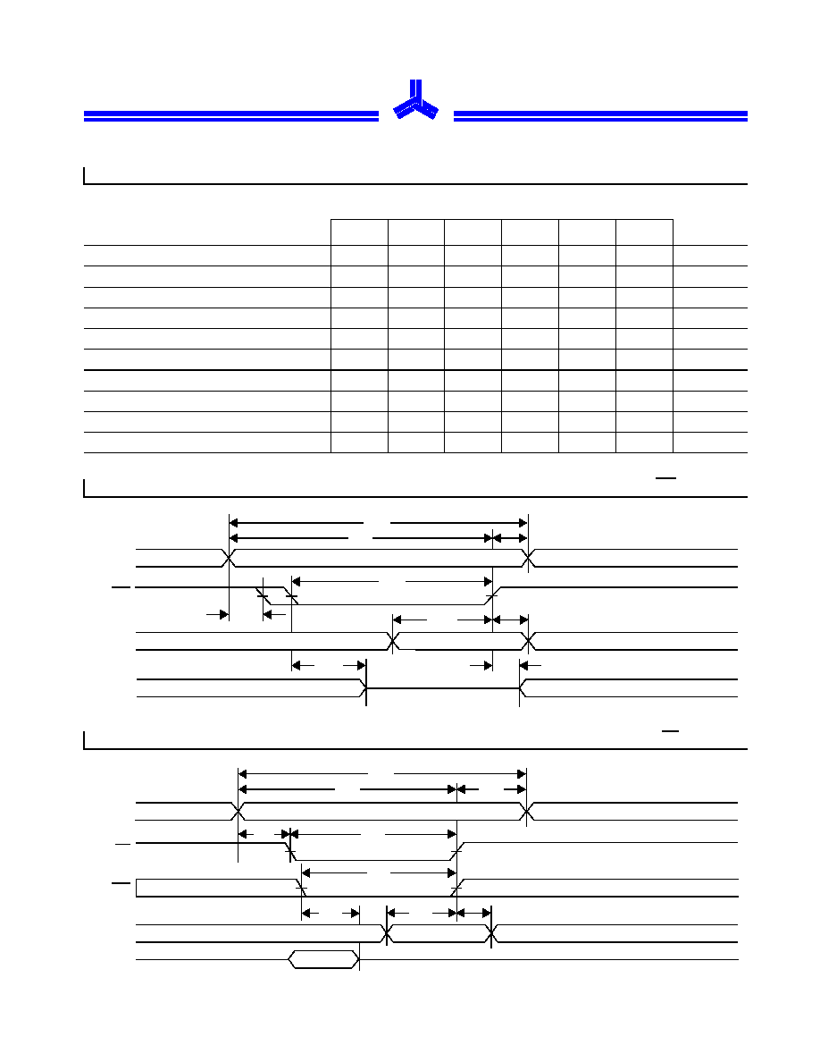
READ CYCLE
(V
CC
= 5V
±
10%, GND = 0V, T
a
= 0∞C to +70∞C)
3, 9
3, 6, 7, 9
TIMING WAVEFORM OF READ CYCLE 1
(Address Controlled)
AAAA
AAAA
AAAA
AAAA
AAAA
AAAA
AAAA
AAAA
AAAA
AAAA
AAAA
AAAA
AAAA
AAAA
AAAA
AAAA
AA
AA
AA
AA
Address
D
out
Data Valid
t
OH
t
AA
t
RC
3, 6, 8, 9
TIMING WAVEFORM OF READ CYCLE 2
(CE Controlled)
AAAA
AAAA
AAAA
AAAA
AAAA
AAAA
AAAA
AAAA
AAAA
AAAA
AAAA
AAAA
Supply
Current
CE
OE
D
out
t
RC
1
t
OE
t
OLZ
t
ACE
t
CHZ
t
CLZ
t
PU
t
PD
I
CC
I
SB
50%
50%
t
OHZ
AAAA
AAAA
AAAA
AAAA
AAAA
AAAA
AAAA
AAAA
AAAA
AAAA
AAAA
AAAA
AAAA
AAAA
AAAA
AAAA
AAAA
AAAA
AAAA
AAAA
AAAA
AAAA
AAAA
AAAA
AAAA
AAAA
AAAA
AAAA
AAAA
AAAA
AAAA
AAAA
AAAA
AAAA
AAAA
AAAA
AAAA
AAAA
AAAA
AAAA
AAAA
AAAA
AAAA
AAAA
AAAA
AAAA
AAAA
AAAA
AAAA
AAAA
AAAA
AAAA
AAAA
AAAA
AAAA
AAAA
AAAA
AAAA
AAAA
AAAA
AAAA
AAAA
AAAA
AAAA
AAAA
AAAA
AAAA
AAAA
AAAA
AAAA
AAAA
AAAA
AAAA
AAAA
AAAA
AA
AA
AA
AA
AA
Data Valid
AAAA
AAAA
AAAA
AAAA
AAAA
AAAA
AAAA
AAAA
AAAA
AAAA
AAAA
AAAA
AAAA
AAAA
AAAA
AAAA
AAAA
AAAA
AAAA
AAAA
AAAA
AAAA
AAAA
AAAA
AAAA
AAAA
AAAA
AAAA
AAAA
AAAA
A
A
A
A
A
AS7C256-04
AS7C256
AS7C256L
5
Parameter
Symbol
-10
-12
-15
-20
-25
-35
Unit
Notes
Min Max Min Max Min Max Min Max Min Max Min Max
Write Cycle Time
t
WC
10
≠
12
≠
15
≠
20
≠
20
≠
30
≠
ns
Chip Enable to Write End
t
CW
9
≠
10
≠
12
≠
12
≠
15
≠
20
≠
ns
Address Setup to Write End
t
AW
9
≠
10
≠
12
≠
12
≠
15
≠
20
≠
ns
Address Setup Time
t
AS
0
≠
0
≠
0
≠
0
≠
0
≠
0
≠
ns
Write Pulse Width
t
WP
7
≠
8
≠
9
≠
12
≠
15
≠
17
≠
ns
Address Hold From End of Write
t
AH
0
≠
0
≠
0
≠
0
≠
0
≠
0
≠
ns
Data Valid to Write End
t
DW
6
≠
6
≠
8
≠
10
≠
10
≠
15
≠
ns
Data Hold Time
t
DH
0
≠
0
≠
0
≠
0
≠
0
≠
0
≠
ns
4, 5
Write Enable to Output in High Z
t
WZ
≠
5
≠
5
≠
5
≠
5
≠
5
≠
5
ns
4, 5
Output Active from Write End
t
OW
3
≠
3
≠
3
≠
3
≠
3
≠
3
≠
ns
4, 5
11
WRITE CYCLE
(V
CC
= 5V
±
10%, GND = 0V, T
a
= 0∞C to +70∞C)
10, 11
TIMING WAVEFORM OF WRITE CYCLE 1
(WE Controlled)
t
AW
t
AH
t
WC
AAAA
AAAA
AAAA
AAAA
AAAA
AAAA
AAAA
AAAA
AAAA
AAAA
AA
AA
AA
AA
AA
Address
WE
D
in
D
out
t
DH
t
OW
t
DW
t
WZ
t
WP
t
AS
Data Valid
AS7C256-05
10, 11
TIMING WAVEFORM OF WRITE CYCLE 2
(CE Controlled)
t
AW
AAAA
AAAA
AAAA
AAAA
AAAA
AAAA
AAAA
AAAA
AAAA
AAAA
AAAA
AAAA
AAAA
AAAA
AAAA
AAAA
AAAA
AAAA
AAAA
AAAA
AAAA
AAAA
AAAA
AAAA
AAAA
AAAA
AAAA
AAAA
AAAA
AAAA
AAAA
AAAA
AAAA
AAAA
AAAA
AAAA
AAAA
AAAA
AAAA
AAAA
AAAA
AAAA
AAAA
AAAA
AAAA
AAAA
AAAA
AAAA
AAAA
AAAA
AAAA
AAAA
AAAA
AAAA
AAAA
AAAA
AAAA
AAAA
AAAA
AAAA
AAAA
AAAA
AAAA
AAAA
AAAA
AAAA
AAAA
AAAA
AAAA
AAAA
AA
AA
AA
AA
AA
AAAA
AAAA
AAAA
AAAA
AAAA
AAAA
AAAA
AAAA
AAAA
AAAA
AAAA
AAAA
AAAA
AAAA
AAAA
AAAA
AAAA
AAAA
AAAA
AAAA
AAAA
AAAA
AAAA
AAAA
AAAA
AAAA
AAAA
AAAA
AAAA
AAAA
AAAA
AAAA
AAAA
AAAA
AAAA
AAAA
AAAA
AAAA
AAAA
AAAA
AAA
AAA
AAA
AAA
AAA
Address
CE
WE
D
in
D
out
Data Valid
t
CW
t
WP
t
DW
t
DH
t
AH
t
WZ
t
WC
AAAA
AAAA
AAAA
AAAA
AAAA
AAAA
AAAA
AAAA
AAAA
AAAA
AAAA
AAAA
AAAA
AAAA
AAAA
AAA
AAA
AAA
AAA
AAA
t
AS
AS7C256-06