
Copyright ©Alliance Semiconductor. All rights reserved.
Æ
AS4C1M16E5
4/11/01; v.1.0
Alliance Semiconductor
P.
1 of 22
5V 1M◊16 CMOS DRAM (EDO)
Features
∑ Organization: 1,048,576 words ◊ 16 bits
∑ High speed
- 45/50/60 ns RAS access time
- 20/20/25 ns hyper page cycle time
- 10/12/15 ns CAS access time
∑ Low power consumption
- Active:
740 mW max (AS4C1M16E5-60)
- Standby: 5.5 mW max, CMOS DQ
∑ Extended data out
∑ 1024 refresh cycles, 16 ms refresh interval
- RAS-only or CAS-before-RAS refresh Read-modify-write
∑ TTL-compatible, three-state DQ
∑ JEDEC standard package and pinout
- 400 mil, 42-pin SOJ
- 400 mil, 44/50-pin TSOP II
∑ 5V power supply (AS4C1M16E5)
∑ 3V power supply (AS4LC1M16E5)
∑ Industrial and commercial temperature available
Pin arrangement
42
41
40
39
38
37
36
35
34
33
V
SS
DQ16
DQ15
DQ14
DQ13
V
SS
DQ12
DQ11
DQ10
DQ9
SOJ
32
31
30
29
28
27
26
25
24
23
NC
LCAS
UCAS
OE
A9
A8
A6
A5
A4
V
SS
1
2
3
4
5
6
7
8
9
10
Vcc
DQ1
DQ2
DQ3
DQ4
Vcc
DQ5
DQ6
DQ7
DQ8
11
12
13
14
15
16
17
18
19
20
NC
NC
WE
RAS
NC
NC
A0
A1
A2
A3
22
21
Vcc
A7
V
CC
DQ1
DQ2
DQ3
DQ4
V
CC
DQ5
DQ6
DQ7
DQ8
NC
NC
V
SS
DQ16
DQ15
DQ14
DQ13
V
SS
DQ12
DQ11
DQ10
DQ9
NC
NC
LCAS
UCAS
OE
50
49
48
47
46
45
44
43
42
41
40
36
35
34
33
32
31
30
29
1
2
3
4
5
6
7
8
9
10
11
15
16
17
18
19
20
21
22
TSOP II
23
24
25
28
27
26
NC
WE
RAS
NC
NC
A0
A1
A2
A3
V
CC
A9
A8
A7
A6
A5
A4
V
SS
Pin designation
Pin(s)
Description
A0 to A9
Address inputs
RAS
Row address strobe
DQ1 to DQ16
Input/output
OE
Output enable
WE
Write enable
UCAS
Column address strobe, upper byte
LCAS
Column address strobe, lower byte
V
CC
Power
V
SS
Ground
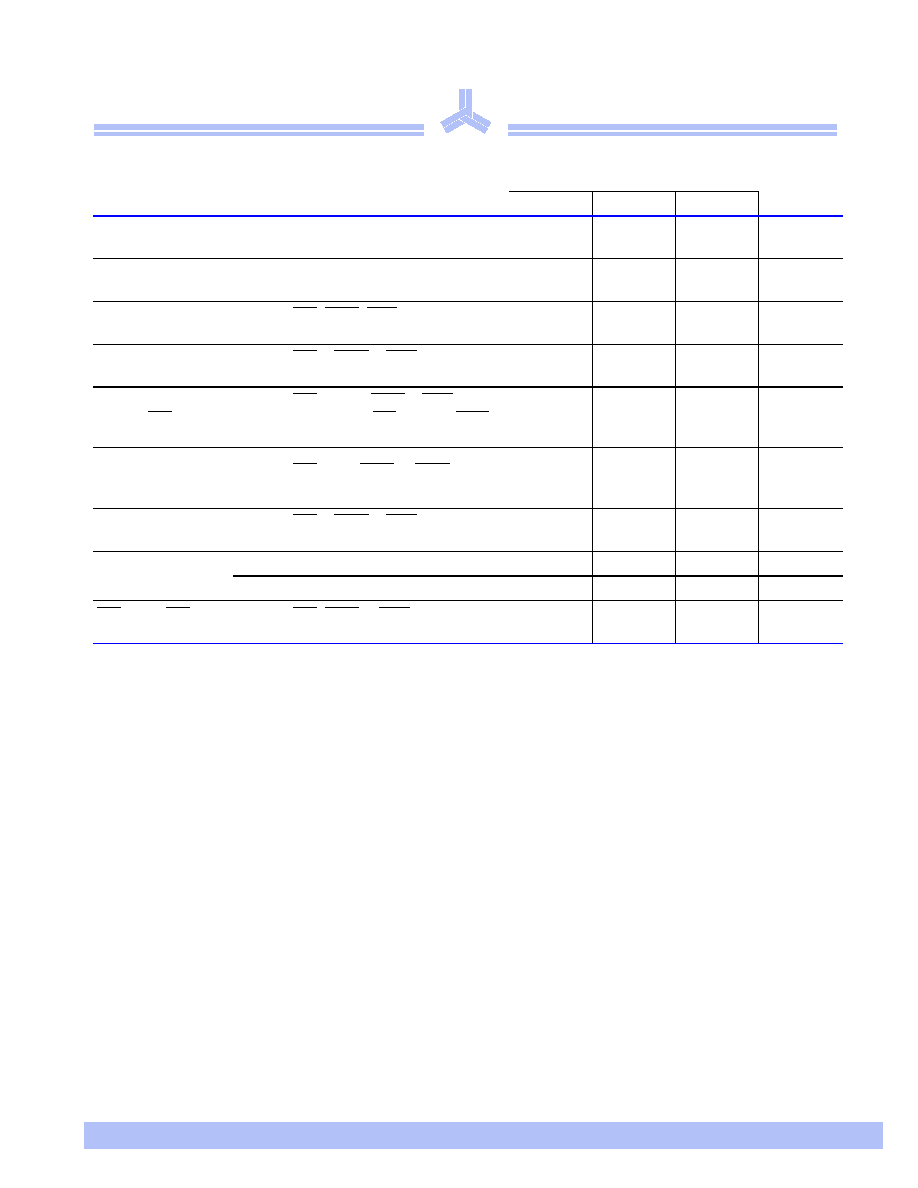
Selection guide
Symbol
-45
-50
-60
Unit
Maximum RAS access time
t
RAC
45
50
60
ns
Maximum column address access time
t
AA
23
25
30
ns
Maximum CAS access time
t
CAC
10
12
15
ns
Maximum output enable (OE) access time
t
OEA
12
13
15
ns
Minimum read or write cycle time
t
RC
75
80
100
ns
Minimum hyper page mode cycle time
t
HPC
20
20
25
ns
Maximum operating current
I
CC1
155
145
135
mA
Maximum CMOS standby current
I
CC5
1.0
1.0
1.0
mA

Æ
AS4C1M16E5
4/11/01; v.1.0
Alliance Semiconductor
P.
2 of 22
Functional description
The AS4C1M16E5 is a high performance 16-megabit CMOS Dynamic Random Access Memory (DRAM) organized as 1,048,576 words ◊ 16
bits. The device is fabricated using advanced CMOS technology and innovative design techniques resulting in high speed, extremely low
power and wide operating margins at component and system levels. The Alliance 16Mb DRAM family is optimized for use as main memory
in personal and portable PCs, workstations, and multimedia and router switch applications.
The AS4C1M16E5 features hyper page mode operation where read and write operations within a single row (or page) can be executed at
very high speed by toggling column addresses within that row. Row and column addresses are alternately latched into input buffers using the
falling edge of RAS and xCAS inputs, respectively. Also, RAS is used to make the column address latch transparent, enabling application of
column addresses prior to xCAS assertion. The AS4C1M16E5 provides dual UCAS and LCAS for independent byte control of read and write
access.
Extended data out (EDO), also known as 'hyper-page mode,' enables high speed operation. In contrast to 'fast-page mode' devices, data
remains active on outputs after xCAS is de-asserted high, giving system logic more time to latch the data. Use OE and WE to control output
impedance and prevent bus contention during read-modify-write and shared bus applications. Outputs also go to high impedance at the last
occurrance of RAS and xCAS going high.
Refresh on the 1024 address combinations of A0 to A9 must be performed every 16 ms using:
∑ RAS-only refresh: RAS is asserted while xCAS is held high. Each of the 1024 rows must be strobed. Outputs remain high impedence.
∑ Hidden refresh: xCAS is held low while RAS is toggled. Outputs remain low impedence with previous valid data.
∑ CAS-before-RAS refresh (CBR): At least one xCAS is asserted prior to RAS. Refresh address is generated internally.
Outputs are high-impedence (OE and WE are don't care).
∑ Normal read or write cycles refresh the row being accessed.
The AS4C1M16E5 is available in the standard 42-pin plastic SOJ and 44/50-pin TSOP II packages, respectively. The AS4C1M16E5 device
operates with a single power supply of 5V ± 0.5V and provides TTL compatible inputs and outputs.
Logic block diagram
Recommended operating conditions
V
IL
min -3.0V for pulse widths less than 5 ns.
Recommended operating conditions apply throughout this document unless otherwise specified.
Parameter
Symbol
Min
Nominal
Max
Unit
Supply voltage
V
CC
4.5
5.0
5.5
V
GND
0.0
0.0
0.0
V
Input voltage
V
IH
2.4
≠
V
CC
V
V
IL
≠0.5
≠
0.8
V
Ambient operating temperature
Commercial
T
A
0
≠
70
∞C
Industrial
-40
≠
85
RAS clock
generator
Ref
r
es
h
co
n
t
r
o
ll
e
r
1024 ◊ 1024 ◊ 16
Array
(16,777,216)
Sense amp
A0
A1
A2
A3
A4
A5
A6
A7
V
CC
GND
Ad
d
r
e
ss b
u
f
f
ers
A8
R
o
w
de
c
o
de
r
Column decoder
Substrate bias
generator
Data
DQ
buffers
OE
RAS
UCAS
WE clock
generator
WE
LCAS
DQ1 to DQ16
CAS clock
generator
A9
Æ
AS4C1M16E5
4/11/01; v.1.0
Alliance Semiconductor
P.
4 of 22
DC electrical characteristics
Parameter
Symbol Test conditions
-45
-50
-60
Unit Notes
Min
Max
Min
Max
Min
Max
Input leakag
e c
urrent
I
IL
0V
V
in
V
CC
(max)
Pins not under test = 0V
-5
+5
-5
+5
-5
+5
µ
A
Output leakage
current
I
OL
D
OUT
disabled, 0V
V
out
V
CC
(max)
-5
+5
-5
+5
-5
+5
µ
A
Operating power
supply current
I
CC1
RAS, UCAS, LCAS, Address cycling;
t
RC
=min
≠
155
≠
145
≠
135
mA
4,5
TTL standby power
supply current
I
CC2
RAS = UCAS = LCAS
V
IH
,
all other inputs at V
IH
or V
IL
≠
2.0
≠
2.0
≠
2.0
mA
Average power supply
current, RAS refresh
mode or CBR
I
CC3
RAS cycling, UCAS = LCAS
V
IH
,
t
RC
= min of RAS low after XCAS
low.
≠
145
≠
135
≠
125
mA
4
EDO page mode
average power supply
current
I
CC4
RAS = V
IL
, UCAS or LCAS,
address cycling: t
HPC
= min
≠
130
≠
120
≠
110
mA
4, 5
CMOS standby power
supply current
I
CC5
RAS = UCAS = LCAS = V
CC
- 0.2V,
F = 0
≠
1.0
≠
1.0
≠
1.0
mA
Output voltage
V
OH
I
OUT
= -5.0 mA
2.4
≠
2.4
≠
2.4
≠
V
V
OL
I
OUT
= 4.2 mA
≠
0.4
≠
0.4
≠
0.4
V
CAS before RAS
refresh current
I
CC6
RAS, UCAS or LCAS cycling, t
RC
=
min
≠
155
≠
145
≠
135
mA

Æ
AS4C1M16E5
4/11/01; v.1.0
Alliance Semiconductor
P.
5 of 22
AC parameters common to all waveforms
Read cycle
Symbol
Parameter
-45
-50
-60
Unit
Notes
Min
Max
Min
Max
Min
Max
t
RC
Random read or write cycle time
75
≠
80
≠
100
≠
ns
t
RP
RAS precharge time
30
≠
30
≠
40
≠
ns
t
RAS
RAS pulse width
45
10K
50
10K
60
10K
ns
t
CAS
CAS pulse width
8
10K
8
10K
10
10K
ns
t
RCD
RAS to CAS delay time
15
35
15
35
15
43
ns
9
t
RAD
RAS to column address delay time
8
25
9
25
10
30
ns
10
t
RSH
CAS to RAS hold time
10
≠
10
≠
10
≠
ns
t
CSH
RAS to CAS hold time
40
≠
40
≠
50
≠
ns
t
CRP
CAS to RAS precharge time
5
≠
5
≠
5
≠
ns
t
ASR
Row address setup time
0
≠
0
≠
0
≠
ns
t
RAH
Row address hold time
8
≠
8
≠
10
≠
ns
t
T
Transition time (rise and fall)
1
50
1
50
1
50
ns
7,8
t
REF
Refresh period
≠
16
≠
16
≠
16
ms
6
t
CP
CAS precharge time
8
≠
8
≠
10
≠
ns
t
RAL
Column address to RAS lead time
25
≠
25
≠
30
≠
ns
t
ASC
Column address setup time
0
≠
0
≠
0
≠
ns
t
CAH
Column address hold time
8
≠
8
≠
10
≠
ns
Symbol
Parameter
-45
-50
-60
Unit
Notes
Min
Max
Min
Max
Min
Max
t
RAC
Access time from RAS
≠
45
≠
50
≠
60
ns
9
t
CAC
Access time from CAS
≠
10
≠
12
≠
15
ns
9,16
t
AA
Access time from address
≠
23
≠
25
≠
30
ns
10,16
t
RCS
Read command setup time
0
≠
0
≠
0
≠
ns
t
RCH
Read command hold time to CAS
0
≠
0
≠
0
≠
ns
12
t
RRH
Read command hold time to RAS
0
≠
0
≠
0
≠
ns
12
