
$XJXVW
&RS\ULJKW $OOLDQFH 6HPLFRQGXFWRU $OO ULJKWV UHVHUYHG
$6&0(4
0 [ &026 4XDG&$6 '5$0 ('2� IDPLO\
Y
$OOLDQFH 6HPLFRQGXFWRU
3 RI
3LQ DUUDQJHPHQW
$
$
$
$
$
$
$
$
$
$
9
&&
*1'
*1'
,2
,2
&$6
2(
9
&&
,2
,2
:(
5$6
1&
$
62-
A
S
4C
4M4E1
$
$
$
$
$
$
$
$
$
$
9
&&
*1'
*1'
,2
,2
&$6
2(
9
&&
,2
,2
:(
5$6
1&
$
7623
A
S
4C
4M4E1
&$6
&$6
&$6
1&
&$6
&$6
1&
&$6
3LQ GHVLJQDWLRQ
Pin(s)
Description
A0 to A11
Address inputs
RAS
Row address strobe
CAS
Column address strobe
WE
Write enable
I/O0 to I/O3
Input/output
OE
Output enable
V
CC
Power
GND
Ground
NC
No Connection
)HDWXUHV
∑ Organization: 4,194,304 words ◊ 4 bits
∑ High speed
- 50/60 ns RAS access time
- 25/30 ns column address access time
- 12/15 ns CAS access time
∑ Low power consumption
- Active: 495 mW max
- Standby: 5.5 mW max, CMOS I/O
∑ Extended data out
∑ Refresh
- 2048 refresh cycles, 32 ms refresh interval for
AS4C4M4E1Q
- RAS-only and hidden refresh or CAS-before-RAS refresh
TTL-compatible
∑ 4 separate CAS pins allow for separate I/O operation
∑ JEDEC standard package
- 300 mil, 28-pin SOJ
- 300 mil, 28-pin TSOP
∑ 5V power supply
∑ Latch-up current
200 mA
∑ ESD protection
2000 V
6HOHFWLRQ JXLGH
Symbol
AS4C4M4E1Q-50
AS4C4M4E1Q-60
Unit
Maximum RAS access time
t
RAC
50
60
ns
Maximum column address access time
t
CAA
25
30
ns
Maximum CAS access time
t
CAC
12
15
ns
Maximum output enable (OE) access time
t
OEA
13
15
ns
Minimum read or write cycle time
t
RC
85
100
ns
Minimum hyper page mode cycle time
t
PC
20
24
ns
Maximum operating current
I
CC1
135
120
mA
Maximum CMOS standby current
I
CC5
2.0
2.0
mA
$6&0(4
Y
$OOLDQFH 6HPLFRQGXFWRU
3 RI
)XQFWLRQDO GHVFULSWLRQ
The AS4C4M4E1Q is a high performance 16-megabit CMOS Quad CAS Dynamic Random Access Memories (DRAM) organized as 4,194,304
words ◊ 4 bits. The devices are fabricated using advanced CMOS technology and innovative design techniques resulting in high speed,
extremely low power and wide operating margins at component and system levels. The Alliance 16Mb DRAM family is optimized for use as
main memory in PC, workstation, router and switch applications.
This product features a high speed page mode operation where read and write operations within a single row (or page) can be executed at
very high speed by toggling column addresses within that row. Row and column addresses are alternately latched into input buffers using the
falling edge of RAS and CAS inputs respectively. Also, RAS is used to make the column address latch transparent, enabling application of
column addresses prior to CAS assertion.
Extended data out (EDO) read mode enables 50 MHz operation using 50 ns devices. Four individual CAS pins allow for separate I/O
operation which enables the device to operate in parity mode. In contrast to 'fast page mode' devices, data remains active on outputs after
CAS is de-asserted high, giving system logic more time to latch the data. Use OE and WE to control output impedance and prevent bus
contention during read-modify-write and shared bus applications. Outputs also go to high impedance at the last occurrance of RAS and CAS
going high.
Refresh on the 2048 address combinations of A0 to A10 must be performed every 32 ms using:
∑ RAS-only refresh: RAS is asserted while CAS is held high. Each of the 2048 rows must be strobed. Outputs remain high impedence.
∑ Hidden refresh: CAS is held low while RAS is toggled. Refresh address is generated internally. Outputs remain low impedence with
previous valid data.
∑ CAS-before-RAS refresh (CBR): At least one CAS is asserted prior to RAS. Refresh address is generated internally.
Outputs are high-impedence (OE and WE are don't care).
∑ Normal read or write cycles refresh the row being accessed.
The AS4C4M4E1Q is available in the standard 28-pin plastic SOJ and 28-pin plastic TSOP packages. The AS4C4M4E1Q operates with a single
power supply of 5V ± 0.5V. All provide TTL compatible inputs and outputs.
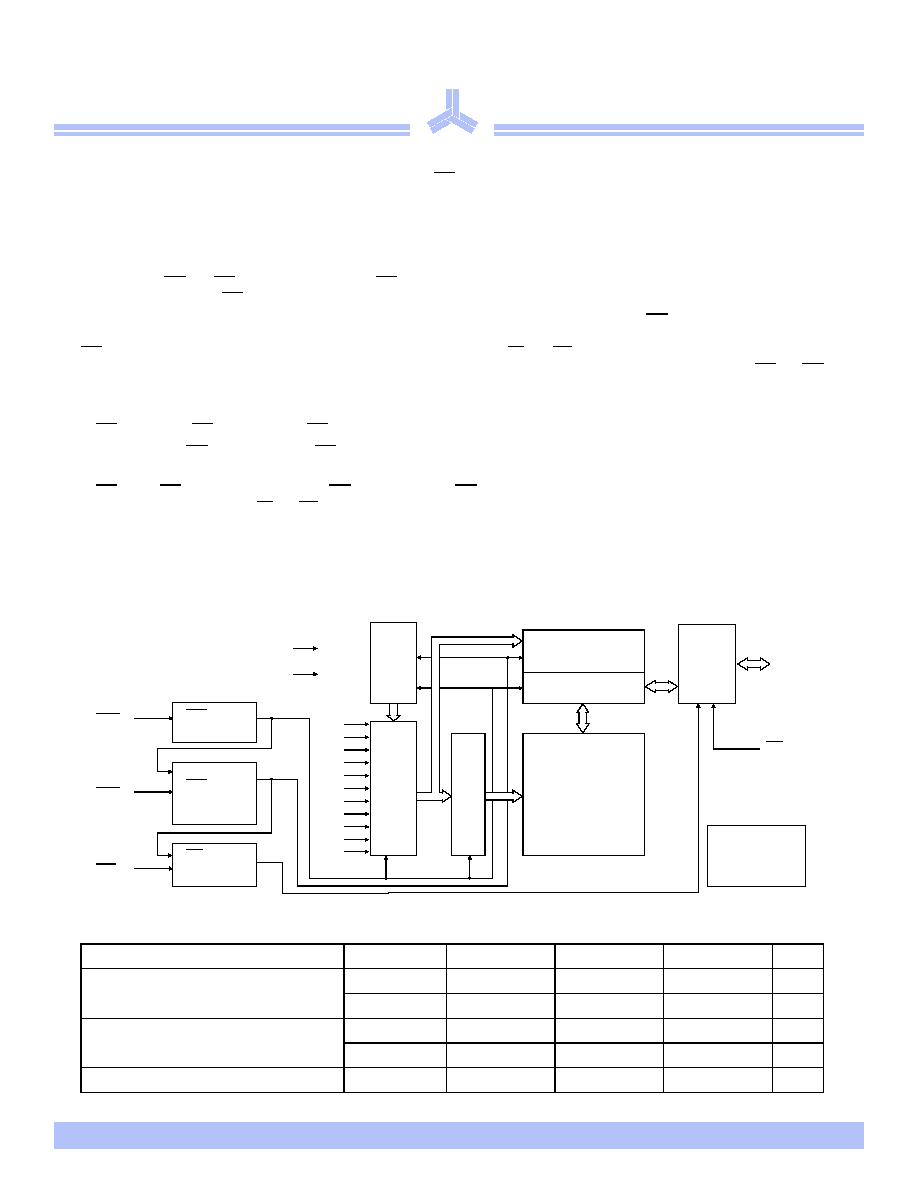
/RJLF EORFN GLDJUDP IRU . UHIUHVK
5HFRPPHQGHG RSHUDWLQJ FRQGLWLRQV
V
IL
min -3.0V for pulse widths less than 5 ns. Recommended operating conditions apply throughout this document unlesss otherwise specified.
Parameter
Symbol
Min
Nominal
Max
Unit
Supply voltage
V
CC
4.5
5.0
5.5
V
GND
0.0
0.0
0.0
V
Input voltage
V
IH
2.4
≠
V
CC
V
V
IL
≠0.5
≠
0.8
V
Ambient operating temperature
T
A
0
70
∞C
5$6 FORFN
JHQHUDWRU
5
H
IUHVK
FRQWURO
O
HU
Ó
$UUD\
�
6HQVH DPS
$
$
$
$
$
$
$
$
9
&&
*1'
$GGU
HVV
EXII
H
U
V
$
5
R
ZGH
FR
GHU
&ROXPQ GHFRGHU
6XEVWUDWH ELDV
JHQHUDWRU
'DWD
,2
EXIIHUV
2(
5$6
&$6
:( FORFN
JHQHUDWRU
:(
,2 WR ,2
&$6 FORFN
JHQHUDWRU
$
$

$6&0(4
Y
$OOLDQFH 6HPLFRQGXFWRU
3 RI
$EVROXWH PD[LPXP UDWLQJV
'& HOHFWULFDO FKDUDFWHULVWLFV $6&0(�
Parameter
Symbol
Min
Max
Unit
Input voltage
V
in
-1.0
+7.0
V
Input voltage (DQs)
V
DQ
-1.0
V
CC
+ 0.5
V
Power supply voltage
V
CC
-1.0
+7.0
V
Storage temperature (plastic)
T
STG
-55
+150
∞C
Soldering temperature ◊ time
T
SOLDER
≠
260 ◊ 10
o
C ◊ sec
Power dissipation
P
D
≠
1
W
Short circuit output current
I
out
≠
50
mA
Parameter
Symbol Test conditions
-50
-60
Unit
Notes
Min
Max
Min
Max
Input leakage current
I
IL
0V
V
in
+5.5V,
Pins not under test = 0V
-5
+5
-5
+5
µA
Output leakage current I
OL
D
OUT
disabled, 0V
V
out
+5.5V
-5
+5
-5
+5
µA
Operating power
supply current
I
CC1
RAS, UCAS, LCAS, Address cycling;
t
RC
=min
≠
135
≠
120
mA
1,2
TTL standby power
supply current
I
CC2
RAS = UCAS = LCAS
V
IH
≠
2.0
≠
2.0
mA
Average power supply
current, RAS refresh
mode or CBR
I
CC3
RAS cycling, UCAS = LCAS
V
IH
,
t
RC
= min of RAS low after XCAS
low.
≠
120
≠
110
mA
1
EDO page mode
average power supply
current
I
CC4
RAS = V
IL
, UCAS or LCAS,
address cycling: t
HPC
= min
≠
130
≠
120
mA
1, 2
CMOS standby power
supply current
I
CC5
RAS = UCAS = LCAS = V
CC
- 0.2V
≠
2.0
≠
2.0
mA
Output voltage
V
OH
I
OUT
= -5.0 mA
2.4
≠
2.4
≠
V
V
OL
I
OUT
= 4.2 mA
≠
0.4
≠
0.4
V
CAS before RAS refresh
current
I
CC6
RAS, UCAS or LCAS cycling, t
RC
=
min
≠
120
≠
110
mA

$6&0(4
Y
$OOLDQFH 6HPLFRQGXFWRU
3 RI
$& SDUDPHWHUV FRPPRQ WR DOO ZDYHIRUPV
5HDG F\FOH
Symbol Parameter
-50
-60
Unit
Notes
Min
Max
Min
Max
t
RC
Random read or write cycle time
80
≠
100
≠
ns
t
RP
RAS precharge time
30
≠
40
≠
ns
t
RAS
RAS pulse width
50
10K
60
10K
ns
t
CAS
CAS pulse width
8
10K
10
10K
ns
t
RCD
RAS to CAS delay time
15
35
15
43
ns
6
t
RAD
RAS to column address delay time
12
25
12
30
ns
7
t
RSH
CAS to RAS hold time
10
≠
10
≠
ns
t
CSH
RAS to CAS hold time
40
≠
50
≠
ns
t
CRP
CAS to RAS precharge time
5
≠
5
≠
ns
t
ASR
Row address setup time
0
≠
0
≠
ns
t
RAH
Row address hold time
8
≠
10
≠
ns
t
T
Transition time (rise and fall)
1
50
1
50
ns
4,5
t
REF
Refresh period
≠
32
≠
32
ms
16
t
CP
CAS precharge time
8
≠
10
≠
ns
t
RAL
Column address to RAS lead time
25
≠
30
≠
ns
t
ASC
Column address setup time
0
≠
0
≠
ns
t
CAH
Column address hold time
8
10
≠
ns
Symbol Parameter
-50
-60
Unit
Notes
Min
Max
Min
Max
t
RAC
Access time from RAS
≠
50
≠
60
ns
6
t
CAC
Access time from CAS
≠
12
≠
15
ns
6,13
t
AA
Access time from address
≠
25
≠
30
ns
7,13
t
RCS
Read command setup time
0
≠
0
≠
ns
t
RCH
Read command hold time to CAS
0
≠
0
≠
ns
9
t
RRH
Read command hold time to RAS
0
≠
0
≠
ns
9

$6&0(4
Y
$OOLDQFH 6HPLFRQGXFWRU
3 RI
:ULWH F\FOH
5HDGPRGLI\ZULWH F\FOH
5HIUHVK F\FOH
Symbol Parameter
-50
-60
Unit
Notes
Min
Max
Min
Max
t
WCS
Write command setup time
0
≠
0
≠
ns
11
t
WCH
Write command hold time
10
≠
10
≠
ns
11
t
WP
Write command pulse width
10
≠
10
≠
ns
t
RWL
Write command to RAS lead time
10
≠
10
≠
ns
t
CWL
Write command to CAS lead time
8
≠
10
≠
ns
t
DS
Data-in setup time
0
≠
0
≠
ns
12
t
DH
Data-in
hold
time
8
≠
10
≠
ns
12
Symbol Parameter
-50
-60
Unit
Notes
Min
Max
Min
Max
t
RWC
Read-write
cycle
time
113
≠
135
≠
ns
t
RWD
RAS to WE delay time
67
≠
77
≠
ns
11
t
CWD
CAS to WE delay time
32
≠
35
≠
ns
11
t
AWD
Column address to WE delay time
42
≠
47
≠
ns
11
Symbol Parameter
-50
-60
Unit
Notes
Min
Max
Min
Max
t
CSR
CAS setup time (CAS-before-RAS)
5
≠
5
≠
ns
3
t
CHR
CAS hold time (CAS-before-RAS)
8
≠
10
≠
ns
3
t
RPC
RAS precharge to CAS hold time
0
≠
0
≠
ns
t
CPT
CAS precharge time
(CBR counter test)
10
10
≠
ns