
Copyright © Alliance Semiconductor. All rights reserved.
Æ
AS4LC4M4F1
4M◊4 CMOS DRAM (Fast Page) 3.3V Family
5/16/01; v.1.0 Restored
Alliance Semiconductor
P. 1 of 14
May 2001
Features
∑ Organization: 4,194,304 words ◊ 4 bits
∑ High speed
- 50/60 ns RAS access time
- 25/30 ns column address access time
- 12/15 ns CAS access time
∑ Low power consumption
- Active:
500 mW max
- Standby: 3.6 mW max, CMOS I/O
∑ Fast page mode
∑ Refresh
- 2048 refresh cycles, 32 ms refresh interval
- RAS-only or CAS-before-RAS refresh or self-refresh
∑ TTL-compatible, three-state I/O
∑ JEDEC standard package
- 300 mil, 24/26-pin SOJ
∑ 3.3V power supply
∑ Latch-up current
200 mA
∑ ESD protection
2000 volts
∑ Industrial and commercial temperature available
Pin arrangement
A8
A7
A6
A5
A4
A10
A0
A1
A2
A3
V
CC
GND
GND
I/O3
I/O2
CAS
OE
V
CC
I/O0
I/O1
WE
RAS
1
2
3
4
5
26
25
24
23
22
NC
A9
6
21
8
9
10
11
18
17
16
15
14
12
SOJ
AS4
L
C4
M
4
F1
A8
A7
A6
A5
A4
A10
A0
A1
A2
A3
V
CC
GND
GND
I/O3
I/O2
CAS
OE
V
CC
I/O0
I/O1
WE
RAS
1
2
3
4
5
NC
A9
6
TSOP*
AS4
L
C4
M
4
F1
13
19
*TSOP availability to be determined
8
9
10
11
12
13
18
17
16
15
14
19
26
25
24
23
22
21
Pin designation
Pin(s)
Description
A0 to A10
Address inputs
RAS
Row address strobe
CAS
Column address strobe
WE
Write enable
I/O0 to I/O3
Input/output
OE
Output enable
V
CC
Power
GND
Ground
Selection guide
Symbol
AS4LC4M4F1-50
AS4LC4M4F1-60
Unit
Maximum RAS access time
t
RAC
50
60
ns
Maximum column address access time
t
CAA
25
30
ns
Maximum CAS access time
t
CAC
12
15
ns
Maximum output enable (OE) access time
t
OEA
13
15
ns
Minimum read or write cycle time
t
RC
80
100
ns
Minimum fast page mode cycle time
t
PC
25
30
ns
Maximum operating current
I
CC1
120
110
mA
Maximum CMOS standby current
I
CC5
1.0
1.0
mA
AS4LC4M4F1
5/16/01; v.1.0 Restored
Alliance Semiconductor
P. 2 of 14
Æ
Functional description
The AS4LC4M4F1 is a high performance 16-megabit CMOS Dynamic Random Access Memory (DRAM) device organized as 4,194,304
words ◊ 4 bits. The device is fabricated using advanced CMOS technology and innovative design techniques resulting in high speed,
extremely low power and wide operating margins at component and system levels. The Alliance 16Mb DRAM family is optimized for use as
main memory in PC, workstation, router and switch applications.
This device features a high speed page-mode operation where read and write operations within a single row (or page) can be executed at
very high speed by toggling column addresses within that row. Row and column addresses are alternately latched into input buffers using the
falling edge of RAS and CAS inputs respectively. Also, RAS is used to make the column address latch transparent, enabling application of
column addresses prior to CAS assertion.
Refresh on the 2048 address combinations of A0 to A10 must be performed every 32 ms using:
∑ RAS-only refresh: RAS is asserted while CAS is held high. Each of the 2048 rows must be strobed. Outputs remain high impedence.
∑ Hidden refresh: CAS is held low while RAS is toggled. Refresh address is generated internally. Outputs remain low impedence with
previous valid data.
∑ CAS-before-RAS refresh (CBR): CAS is asserted prior to RAS. Refresh address is generated internally.
Outputs are high-impedence (OE and WE are don't care).
∑ Normal read or write cycles refresh the row being accessed.
∑ Self-refresh cycles
The AS4LC4M4F1 is available in the standard 24/26-pin plastic SOJ. TSOP 24/26-pin availability is to be determined. The AS4LC4M4F1
operates with a single power supply of 3.3V ± 0.3V and provides TTL compatible inputs and outputs.
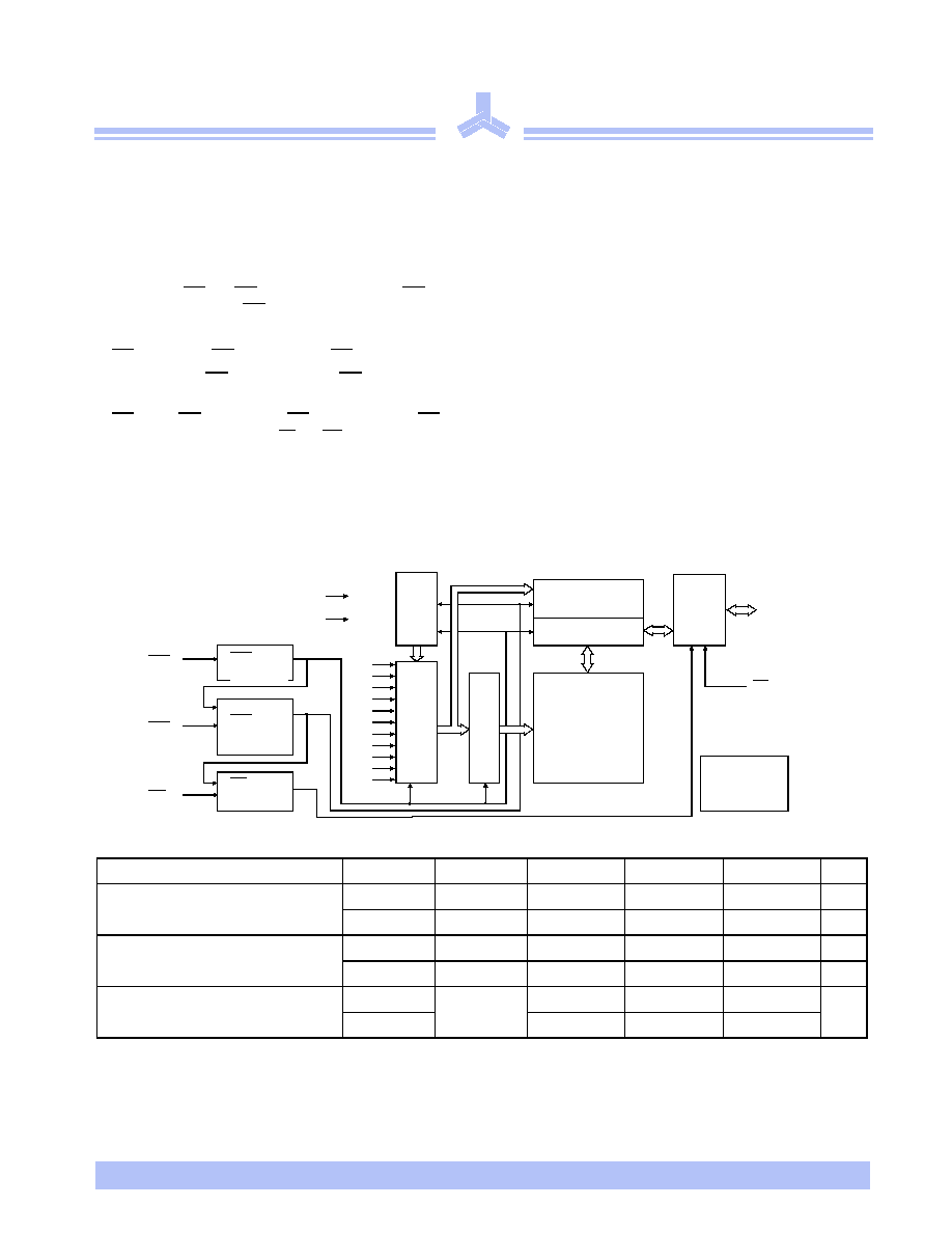
Logic block diagram for 2K refresh
Recommended operating conditions
V
IL
min -3.0V for pulse widths less than 5 ns. Recommended operating conditions apply throughout this document unlesss otherwise specified.
Parameter
Symbol
Min
Nominal
Max
Unit
Supply voltage
V
CC
3.0
3.3
3.6
V
GND
0.0
0.0
0.0
V
Input voltage
V
IH
2.0
≠
V
CC+0.5V
V
V
IL
≠0.5
≠
0.8
V
Ambient operating temperature
Commercial
T
A
0
≠
70
∞C
Industrial
-40
≠
85
RAS clock
generator
Re
f
r
esh
contr
o
l
l
er
2048 ◊ 2048 ◊ 4
Array
(16,777,216)
Sense amp
A0
A1
A2
A3
A4
A5
A6
A7
V
CC
GND
Addr
es
s
b
u
f
f
er
s
A8
R
o
w decoder
Column decoder
Substrate bias
generator
Data
I/O
buffers
OE
RAS
CAS
WE clock
generator
WE
I/O0 to I/O3
CAS clock
generator
A9
A10

AS4LC4M4F1
5/16/01; v.1.0 Restored
Alliance Semiconductor
P. 3 of 14
Æ
Absolute maximum ratings
DC electrical characteristics
Parameter
Symbol
Min
Max
Unit
Input voltage
V
in
-1.0
4.6
V
Input voltage (DQs)
V
DQ
-1.0
4.6
V
Power supply voltage
V
CC
-1.0
4.6
V
Storage temperature (plastic)
T
STG
-55
150
∞C
Soldering temperature ◊ time
T
SOLDER
≠
260 ◊ 10
o
C ◊ sec
Power dissipation
P
D
≠
0.432
W
Short circuit output current
I
out
≠
50
mA
Parameter
Symbol
Test conditions
-50
-60
Unit
Notes
Min
Max
Min
Max
Input leakage current
I
IL
0V
V
in
+V
cc
(max)
Pins not under test = 0V
-5
+5
-5
+5
µA
Output leakage current
I
OL
D
OUT
disabled, 0V
V
out
+ V
cc
(max)
-5
+5
-5
+5
µA
Operating power
supply current
I
CC1
CAS, Address cycling; t
RC
=min
≠
120
≠
110
mA
1,2
TTL standby power
supply current
I
CC2
RAS = CAS
V
IH
≠
2.0
≠
2.0
mA
Average power supply
current, RAS refresh
mode or CBR
I
CC3
RAS cycling, CAS
V
IH
,
t
RC
= min of RAS low after CAS low.
≠
120
≠
110
mA
1
Fast page mode average
power supply current
I
CC4
RAS = V
IL
, CAS,
address cycling: t
HPC
= min
≠
90
≠
80
mA
1, 2
CMOS standby power
supply current
I
CC5
RAS = CAS = V
CC
- 0.2V
≠
2.0
≠
2.0
mA
Output voltage
V
OH
I
OUT
= -2.0 mA
2.4
≠
2.4
≠
V
V
OL
I
OUT
= 2.0 mA
≠
0.4
≠
0.4
V
CAS before RAS refresh
current
I
CC6
RAS, CAS cycling, t
RC
= min
≠
120
≠
110
mA
Self refresh current
I
CC7
RAS
=
CAS
0.2v,
WE
-
OE
V
CC
- 0.2V,
all other inputs at 0.2V or V
CC
- 0.2V
-
0.6
-
0.6
mA

AS4LC4M4F1
5/16/01; v.1.0 Restored
Alliance Semiconductor
P. 4 of 14
Æ
AC parameters common to all waveforms
Read cycle
Symbol
Parameter
-50
-60
Unit
Notes
Min
Max
Min
Max
t
RC
Random read or write cycle time
80
≠
100
≠
ns
t
RP
RAS precharge time
30
≠
40
≠
ns
t
RAS
RAS pulse width
50
10K
60
10K
ns
t
CAS
CAS pulse width
8
10K
10
10K
ns
t
RCD
RAS to CAS delay time
15
35
15
43
ns
6
t
RAD
RAS to column address delay time
12
25
12
30
ns
7
t
RSH
CAS to RAS hold time
10
≠
10
≠
ns
t
CSH
RAS to CAS hold time
40
≠
50
≠
ns
t
CRP
CAS to RAS precharge time
5
≠
5
≠
ns
t
ASR
Row address setup time
0
≠
0
≠
ns
t
RAH
Row address hold time
8
≠
10
≠
ns
t
T
Transition time (rise and fall)
1
50
1
50
ns
4,5
t
REF
Refresh period
≠
64
≠
64
ms
3
t
CP
CAS precharge time
8
≠
10
≠
ns
t
RAL
Column address to RAS lead time
25
≠
30
≠
ns
t
ASC
Column address setup time
0
≠
0
≠
ns
t
CAH
Column address hold time
8
10
≠
ns
Symbol
Parameter
-50
-60
Unit
Notes
Min
Max
Min
Max
t
RAC
Access time from RAS
≠
50
≠
60
ns
6
t
CAC
Access time from CAS
≠
12
≠
15
ns
6,13
t
AA
Access time from address
≠
25
≠
30
ns
7,13
t
RCS
Read command setup time
0
≠
0
≠
ns
t
RCH
Read command hold time to CAS
0
≠
0
≠
ns
9
t
RRH
Read command hold time to RAS
0
≠
0
≠
ns
9

AS4LC4M4F1
5/16/01; v.1.0 Restored
Alliance Semiconductor
P. 5 of 14
Æ
Write cycle
Read-modify-write cycle
Refresh cycle
Symbol
Parameter
-50
-60
Unit
Notes
Min
Max
Min
Max
t
WCS
Write command setup time
0
≠
0
≠
ns
11
t
WCH
Write command hold time
10
≠
10
≠
ns
11
t
WP
Write command pulse width
10
≠
10
≠
ns
t
RWL
Write command to RAS lead time
10
≠
10
≠
ns
t
CWL
Write command to CAS lead time
8
≠
10
≠
ns
t
DS
Data-in setup time
0
≠
0
≠
ns
12
t
DH
Data-in hold time
8
≠
10
≠
ns
12
Symbol
Parameter
-50
-60
Unit
Notes
Min
Max
Min
Max
t
RWC
Read-write
cycle
time
113
≠
135
≠
ns
t
RWD
RAS to WE delay time
67
≠
77
≠
ns
11
t
CWD
CAS to WE delay time
32
≠
35
≠
ns
11
t
AWD
Column address to WE delay time
42
≠
47
≠
ns
11
Symbol
Parameter
-50
-60
Unit
Notes
Min
Max
Min
Max
t
CSR
CAS setup time (CAS-before-RAS)
5
≠
5
≠
ns
3
t
CHR
CAS hold time (CAS-before-RAS)
8
≠
10
≠
ns
3
t
RPC
RAS precharge to CAS hold time
0
≠
0
≠
ns
t
CPT
CAS precharge time
(CBR counter test)
10
10
≠
ns