November 2000
Copyright ©2000 Alliance Semiconductor. All rights reserved.
Æ
AS7C1024
AS7C31024
11/29/00
ALLIANCE SEMICONDUCTOR
1
5V/3.3V 128K◊8 CMOS SRAM (Evolutionary Pinout)
Features
∑ AS7C1024 (5V version)
∑ AS7C31024 (3.3V version)
∑ Industrial and commercial temperatures
∑ Organization: 131,072 words ◊ 8 bits
∑ High speed
- 10/12/15/20 ns address access time
- 5/6/8/10 ns output enable access time
∑ Low power consumption: ACTIVE
- 825 mW (c) / max @ 12 ns
- 360 mW (AS7C31024) / max @ 12 ns
∑ Low power consumption: STANDBY
- 55 mW (AS7C1024) / max CMOS
- 36 mW (AS7C31024) / max CMOS
∑ 2.0V data retention
∑ Easy memory expansion with CE1, CE2, OE inputs
∑ TTL/LVTTL-compatible, three-state I/O
∑ 32-pin JEDEC standard packages
- 300 mil SOJ
- 400 mil SOJ
- 8 ◊ 20mm TSOP I
- 8 ◊ 13.4 mm sTSOP I
∑ ESD protection
2000 volts
∑ Latch-up current
200 mA
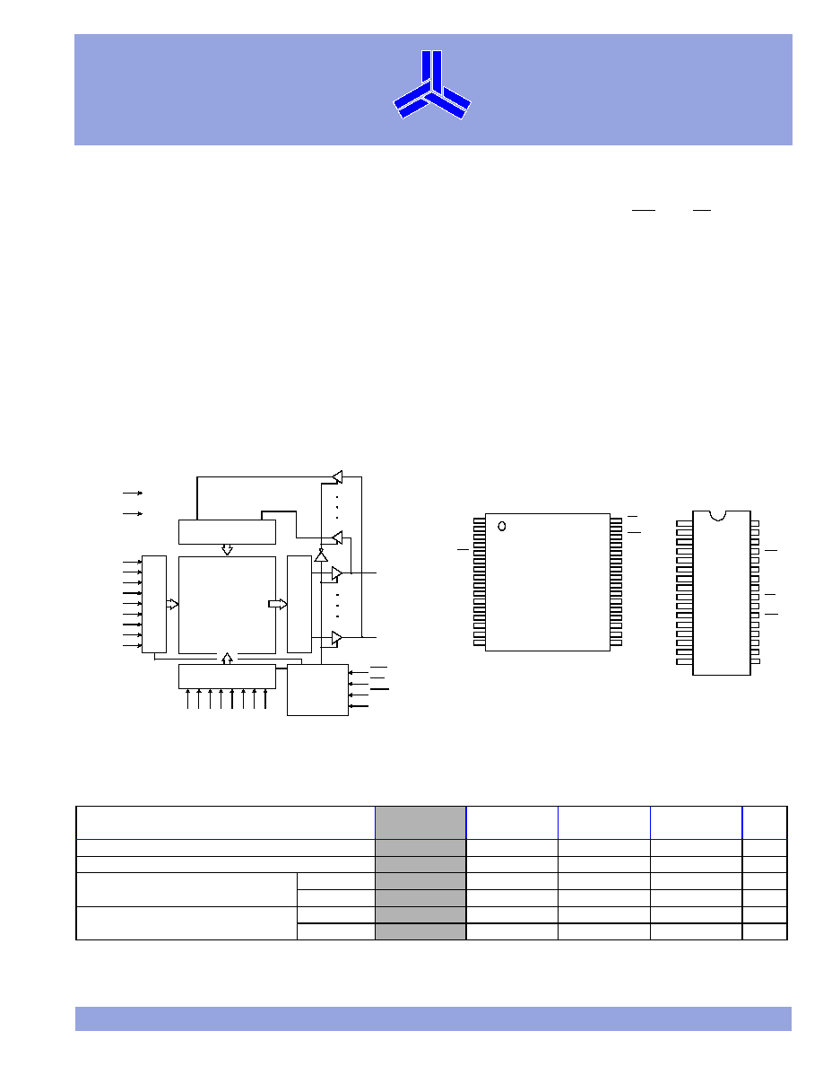
Logic block diagram
512
◊
256
◊
8
Array
(1,048,576)
S
e
n
se a
m
p
Input buffer
A1
0
A1
1
A1
2
A1
3
A1
4
A1
5
A1
6
I/O0
I/O7
OE
CE1
WE
Column decoder
Ro
w
dec
o
d
e
r
Control
circuit
A9
A0
A1
A2
A3
A4
A5
A6
A7
V
CC
GND
A8
CE2
Pin arrangement
1
2
3
4
5
6
7
8
9
10
11
12
13
14
15
16
32
31
30
29
28
27
26
25
24
23
22
21
20
19
18
17
V
CC
A15
CE2
WE
A13
A8
A9
A11
OE
A10
CE1
I/O7
I/O6
I/O5
I/O4
I/O3
NC
A16
A14
A12
A7
A6
A5
A4
A3
A2
A1
A0
I/O0
I/O1
I/O2
GND
32-pin SOJ (300 mil)
V
CC
A15
CE2
WE
A13
A8
A9
A11
OE
A10
CE1
I/O7
I/O6
I/O4
NC
A16
A14
A12
A7
A6
A5
A4
A3
A2
A1
A0
I/O0
I/O1
32-pin TSOP I
I/O2
GND
I/O5
I/O3
1
2
3
4
5
6
7
8
9
10
11
12
13
14
32
31
30
29
28
27
26
25
24
23
22
21
A
S
7C
1024
A
S
7C
31024
20
19
15
16
18
17
(8 x 20mm)
32-pin SOJ (400 mil)
Selection guide
Shaded areas contain advance information.
AS7C1024-10
AS7C31024-10
AS7C1024-12
AS7C31024-12
AS7C1024-15
AS7C31024-15
AS7C1024-20
AS7C31024-20
Unit
Maximum address access time
10
12
15
20
ns
Maximum output enable access time
5
6
8
10
ns
Maximum operating current
AS7C1024
150
140
125
110
mA
AS7C31024
100
90
80
75
mA
Maximum CMOS standby current
AS7C1024
10
10
10
15
mA
AS7C31024
10
10
10
15
mA
Æ
2
ALLIANCE SEMICONDUCTOR
11/29/00
AS7C1024
AS7C31024
Functional description
The AS7C1024 and AS7C31024 are high performance CMOS 1,048,576-bit Static Random Access Memory (SRAM) devices
organized as 131,072 words ◊ 8 bits. It is designed for memory applications where fast data access, low power, and simple
interfacing are desired.
Equal address access and cycle times (t
AA
, t
RC
, t
WC
) of 10/12/15/20 ns with output enable access times (t
OE
) of 5/6/8/10 ns
are ideal for high performance applications. Active high and low chip enables (CE1, CE2) permit easy memory expansion with
multiple-bank systems.
When CE1 is high or CE2 is low the devices enter standby mode. If inputs are still toggling, the device will consume I
SB
power.
If the bus is static, then full standby power is reached (I
SB1
or I
SB2
). For example, the AS7C31024 is guaranteed not to exceed
0.33mW under nominal full standby conditions. All devices in this family will retain data when VCC is reduced as low as 2.0V.
A write cycle is accomplished by asserting write enable (WE) and both chip enables (CE1, CE2). Data on the input pins I/O0-
I/O7 is written on the rising edge of WE (write cycle 1) or the active-to-inactive edge of CE1 or CE2 (write cycle 2). To avoid
bus contention, external devices should drive I/O pins only after outputs have been disabled with output enable ( OE) or write
enable (WE).
A read cycle is accomplished by asserting output enable (OE) and both chip enables (CE1, CE2), with write enable (WE) high.
The chips drive I/O pins with the data word referenced by the input address. When either chip enable is inactive, output
enable is inactive, or write enable is active, output drivers stay in high-impedance mode.
Absolute maximum ratings
Note: Stresses greater than those listed under Absolute Maximum Ratings may cause permanent damage to the device. This is a stress rating only and functional
operation of the device at these or any other conditions outside those indicated in the operational sections of this specificati on is not implied. Exposure to
absolute maximum rating conditions for extended periods may affect reliability.
Truth table
Key: X = Don't Care, L = Low, H = High
Parameter
Symbol
Min
Max
Unit
Voltage on V
CC
relative to GND
AS7C1024
V
t1
≠0.50
+7.0
V
AS7C31024
V
t1
-0.50
+5.0
V
Voltage on any pin relative to GND
V
t2
≠0.50
V
CC
+0.50
V
Power dissipation
P
D
≠
1.0
W
Storage temperature (plastic)
T
stg
≠65
+150
∞
C
Ambient temperature with V
CC
applied
T
bias
≠55
+125
∞
C
DC current into outputs (low)
I
OUT
≠
20
mA
CE1
CE2
WE
OE
Data
Mode
H
X
X
X
High Z
Standby (I
SB
, I
SB1
)
X
L
X
X
High Z
Standby (I
SB
, I
SB1
)
L
H
H
H
High Z
Output disable (I
CC
)
L
H
H
L
D
OUT
Read (I
CC
)
L
H
L
X
D
IN
Write (
ICC
)

Æ
AS7C1024
AS7C31024
11/29/00
ALLIANCE SEMICONDUCTOR
3
Recommended operating conditions
V
IL
min = ≠3.0V for pulse width less than t
RC/2
.
DC operating characteristics (over the operating range)
Shaded areas contain advance information.
Capacitance (f = 1 MHz, T
a
= 25
∞
C, V
CC
= NOMINAL)
Parameter
Device
Symbol
Min
Nominal
Max
Unit
Supply voltage
AS7C1024
V
CC
4.5
5.0
5.5
V
AS7C31024
V
CC
3.0
3.3
3.6
V
Input voltage
AS7C1024
V
IH
2.2
≠
V
CC
+ 0.5
V
AS7C31024
V
IH
2.0
≠
V
CC
+ 0.5
V
V
IL
≠0.5
≠
0.8
V
Ambient operating temperature
commercial
T
A
0
≠
70
∞
C
industrial
T
A
≠40
≠
85
∞
C
Parameter
Sym
Test conditions
Device
-10
-12
-15
-20
Unit
Min Max Min Max Min Max Min Max
Input leakage
current
|I
LI
| V
CC
= Max, V
IN
= GND to V
CC
≠
1
≠
1
≠
1
≠
1
µ
A
Output leakage
current
|I
LO
|
V
CC
= Max, CE1 = V
IH
or
CE2 = V
IL
, V
OUT
= GND to V
CC
≠
1
≠
1
≠
1
≠
1
µ
A
Operating
power supply
current
I
CC
V
CC
= Max, CE1 = V
IL
,
CE2 = V
IH
, f = f
Max
, I
OUT
= 0
mA
AS7C1024
≠
150
≠
140
≠
125
≠
110
mA
AS7C31024
≠
100
≠
90
≠
80
≠
75
Standby power
supply current
I
SB
V
CC
= Max, CE1
V
IH
and/or
CE2
V
IL
, V
IN
= V
IH
or V
IL
,
f = f
Max
, I
OUT
= 0mA
AS7C1024
≠
80
≠
75
≠
65
≠
60
mA
AS7C31024
≠
60
≠
50
≠
40
≠
35
I
SB1
V
CC
= Max, CE1
V
CC
≠0.2V
V
IN
GND + 0.2V or
V
IN
V
CC
≠0.2V, f = 0
AS7C1024
≠
10
≠
10
≠
10
≠
15
mA
AS7C31024
≠
10
≠
10
≠
10
≠
15
Output voltage
V
OL
I
OL
= 8 mA, V
CC
= Min
≠
0.4
≠
0.4
≠
0.4
≠
0.4
V
V
OH
I
OH
= ≠4 mA, V
CC
= Min
2.4
≠
2.4
≠
2.4
≠
2.4
≠
V
Parameter
Symbol
Signals
Test conditions
Max
Unit
Input capacitance
C
IN
A, CE1, CE2, WE, OE
V
IN
= 0V
5
pF
I/O capacitance
C
I/O
I/O
V
IN
= V
OUT
= 0V
7
pF
Æ
4
ALLIANCE SEMICONDUCTOR
11/29/00
AS7C1024
AS7C31024
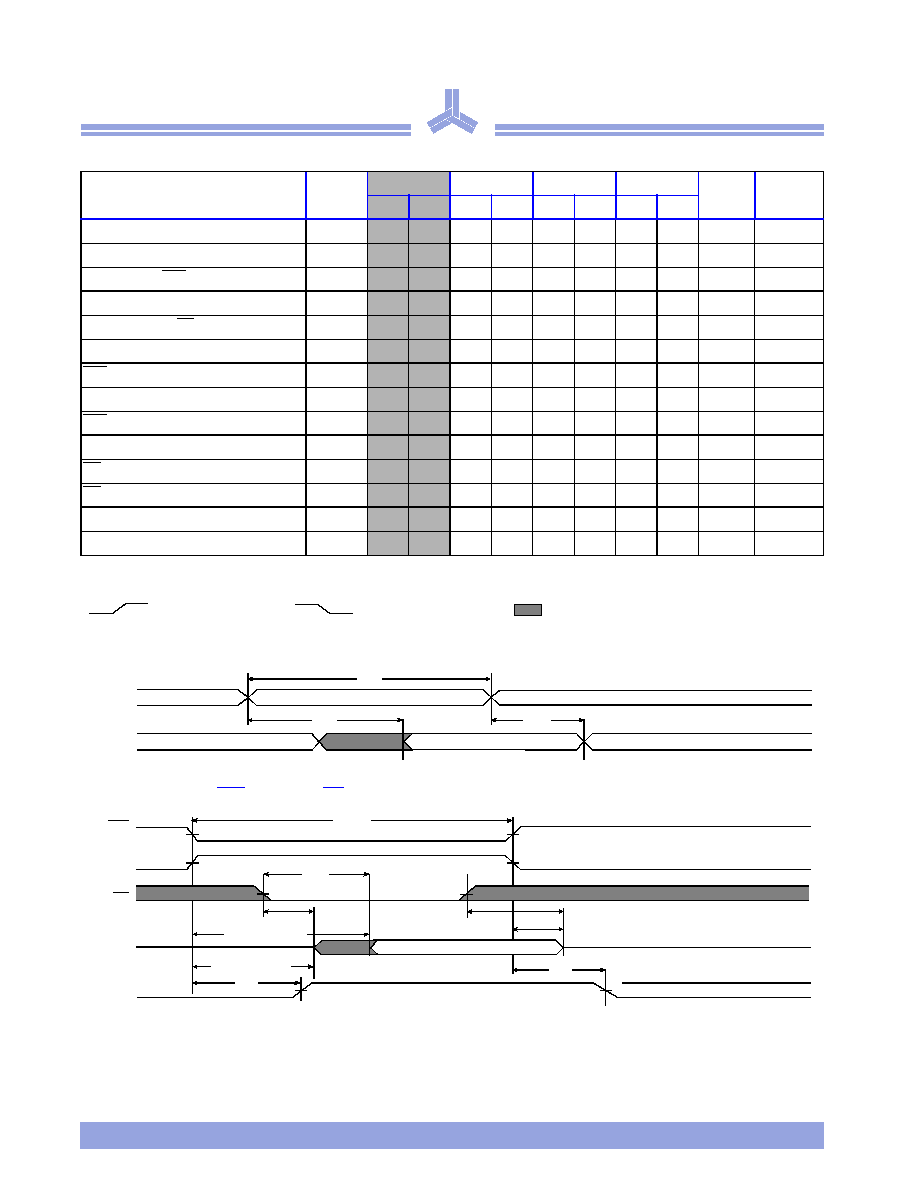
Read cycle (over the operating range)
Key to switching waveforms
Read waveform 1 (address controlled)
Read waveform 2 (CE1, CE2, and OE controlled)
Parameter
Symbol
-10
-12
-15
-20
Unit
Notes
Min
Max
Min
Max
Min
Max
Min
Max
Read cycle time
t
RC
10
≠
12
≠
15
≠
20
≠
ns
Address access time
t
AA
≠
10
≠
12
≠
15
≠
20
ns
3
Chip enable (CE1) access time
t
ACE1
≠
10
≠
12
≠
15
≠
20
ns
3, 12
Chip enable (CE2) access time
t
ACE2
≠
10
≠
12
≠
15
≠
20
ns
3, 12
Output enable (OE) access time
t
OE
≠
3
≠
3
≠
4
≠
5
ns
Output hold from address change
t
OH
2
≠
3
≠
3
≠
3
≠
ns
5
CE1 Low to output in low Z
t
CLZ1
3
≠
3
≠
3
≠
3
≠
ns
4, 5, 12
CE2 High to output in low Z
t
CLZ2
3
≠
3
≠
3
≠
3
≠
ns
4, 5, 12
CE1 Low to output in high Z
t
CHZ1
≠
3
≠
3
≠
4
≠
5
ns
4, 5, 12
CE2 Low to output in high Z
t
CHZ2
≠
3
≠
3
≠
4
≠
5
ns
4, 5, 12
OE Low to output in low Z
t
OLZ
0
≠
0
≠
0
≠
0
≠
ns
4, 5
OE High to output in high Z
t
OHZ
≠
3
≠
3
≠
4
≠
5
ns
4, 5
Power up time
t
PU
0
≠
0
≠
0
≠
0
≠
ns
4, 5, 12
Power down time
t
PD
≠
10
≠
12
≠
15
≠
20
ns
4, 5, 12
Undefined / don't care
Falling input
Rising input
Address
D
OUT
Data valid
t
OH
t
AA
t
RC
supply
Current
CE2
OE
D
OUT
t
OE
t
OLZ
t
ACE1
,
tACE2
t
CHZ1
, t
CHZ2
t
CLZ1
, t
CLZ2
t
PU
t
PD
I
CC
I
SB
50%
50%
Data valid
t
RC1
CE1
t
OHZ

Æ
AS7C1024
AS7C31024
11/29/00
ALLIANCE SEMICONDUCTOR
5
Write cycle (over the operating range)
Shaded areas contain advance information.
Write waveform 1 ( WE controlled)
Write waveform 2 (CE1 and CE2 controlled)
Parameter
Symbol
-10
-12
-15
-20
Unit
Notes
Min
Max
Min
Max
Min
Max
Min
Max
Write cycle time
t
WC
10
≠
12
≠
15
≠
20
≠
ns
Chip enable (CE1) to write end
t
CW1
9
≠
10
≠
12
≠
12
≠
ns
12
Chip enable (CE2) to write end
t
CW2
9
≠
10
≠
12
≠
12
≠
ns
12
Address setup to write end
t
AW
9
≠
10
≠
12
≠
12
≠
ns
Address setup time
t
AS
0
≠
0
≠
0
≠
0
≠
ns
12
Write pulse width
t
WP
7
≠
8
≠
9
≠
12
≠
ns
Address hold from end of write
t
AH
0
≠
0
≠
0
≠
0
≠
ns
Data valid to write end
t
DW
6
≠
6
≠
9
≠
10
≠
ns
Data hold time
t
DH
0
≠
0
≠
0
≠
0
≠
ns
4, 5
Write enable to output in high Z
t
WZ
≠
5
≠
5
≠
5
≠
5
ns
4, 5
Output active from write end
t
OW
3
≠
3
≠
3
≠
3
≠
ns
4, 5
t
AW
t
AH
t
WC
Address
WE
D
OUT
t
DH
t
OW
t
DW
t
WZ
t
WP
t
AS
Data valid
D
IN
t
AW
Address
CE1
WE
D
OUT
t
CW1
, t
CW2
t
WP
t
DW
t
DH
t
AH
t
WZ
t
WC
t
AS
CE2
Data valid
D
IN