May 2002
Copyright © Alliance Semiconductor. All rights reserved.
Æ
AS7C1025A
AS7C31025A
5V/3.3V 128K X 8 CMOS SRAM (Revolutionary pinout)
9/26/02; v.0.9.8
Alliance Semiconductor
P. 1 of 8
Features
∑ AS7C1025A (5V version)
∑ AS7C31025A (3.3V version)
∑ Industrial and commercial temperatures
∑ Organization: 131,072 x 8 bits
∑ High speed
- 10/12/15/20 ns address access time
- 5, 6, 7, 8 ns output enable access time
∑ Low power consumption: ACTIVE
- 853 mW (AS7C1025A) / max @ 10 ns (5V)
- 522 mW (AS7C31025A) / max @ 10 ns (3.3V)
∑ Low power consumption: STANDBY
- 55 mW (AS7C1025A) / max CMOS (5V)
- 36 mW (AS7C31025A) / max CMOS (3.3V)
∑ Latest 6T 0.25u CMOS technology
∑ Easy memory expansion with CE, OE inputs
∑ Center power and ground
∑ TTL/LVTTL-compatible, three-state I/O
∑ JEDEC-standard packages
- 32-pin, 300 mil SOJ
- 32-pin, 400 mil SOJ
- 32-pin, TSOP 2
∑ ESD protection
2000 volts
∑ Latch-up current
200 mA
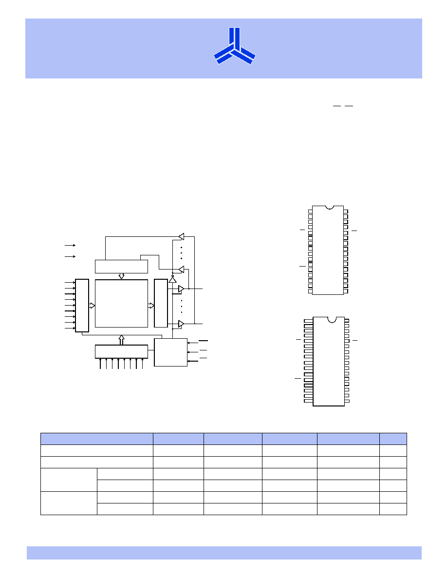
Logic block diagram
512
◊
256
◊
8
Array
(1,048,576)
Se
nse am
p
Input buffer
A10
A11
A12
A13
A14
A15
A16
I/O0
I/O7
OE
CE
WE
Column decoder
R
o
w deco
der
Control
circuit
A9
A0
A1
A2
A3
A4
A5
A6
A7
V
CC
GND
A8
Pin arrangement
1
2
3
4
5
6
7
8
9
10
11
12
13
14
15
16
32
31
30
29
28
27
26
25
24
23
22
21
20
19
18
17
A16
A15
A14
A13
OE
I/O7
I/O6
GND
V
CC
I/O5
I/O4
A12
A11
A10
A9
A8
A0
A1
A2
A3
CE
I/O0
I/O1
V
CC
GND
I/O2
I/O3
WE
A4
A5
A6
A7
AS7C1025A
AS7C3102
5A
32-pin SOJ (300 mil)
32-pin SOJ (400 mil)
1
2
3
4
5
6
7
8
9
10
11
12
13
14
15
16
32
31
30
29
28
27
26
25
24
23
22
21
20
19
18
17
A0
A1
A2
A3
CE
I/O0
I/O1
V
CC
GND
I/O2
I/O3
WE
A16
A15
A14
A13
OE
I/O7
I/O6
GND
V
CC
I/O5
I/O4
A9
A8
A4
A5
A6
A7
A12
A11
A10
32-pin TSOP 2
AS7C1025A
AS7C310
25A
Selection guide
-10
-12
-15
-20
Unit
Maximum address access time
10
12
15
20
ns
Maximum output enable access time
5
6
7
8
ns
Maximum
operating current
AS7C1025A
155
150
145
140
mA
AS7C31025A
145
140
135
130
mA
Maximum CMOS
standby current
AS7C1025A
10
10
10
10
mA
AS7C31025A
5
5
5
5
mA
AS7C1025A
AS7C31025A
9/26/02; v.0.9.8
Alliance Semiconductor
P. 2 of 8
Æ
Functional description
The AS7C1025A and AS7C31025A are high-performance CMOS 1,048,576-bit Static Random Access Memory (SRAM) devices organized as
131,072 x 8 bits. They are designed for memory applications where fast data access, low power, and simple interfacing are desired.
Equal address access and cycle times (t
AA
, t
RC
, t
WC
) of 10/12/15/20 ns with output enable access times (t
OE
) of 5, 6, 7, 8 ns are ideal for
high-performance applications. The chip enable input CE permits easy memory and expansion with multiple-bank memory systems.
When CE is high the devices enter standby mode. The standard AS7C1025A is guaranteed not to exceed 55 mW power consumption in standby
mode.
A write cycle is accomplished by asserting write enable (WE) and chip enable (CE). Data on the input pins I/O0-I/O7 is written on the rising
edge of WE (write cycle 1) or CE (write cycle 2). To avoid bus contention, external devices should drive I/O pins only after outputs have been
disabled with
RXWSXW HQDEOH
OE
� RU ZULWH HQDEOH
(WE).
A read cycle is accomplished by asserting output enable (OE) and chip enable (CE), with write enable (WE) high. The chips drive I/O pins
with the data word referenced by the input address. When either chip enable or output enable is inactive, or write enable is active, output
drivers stay in high-impedance mode.
All chip inputs and outputs are TTL-compatible, and operation is from a single 5V supply (AS7C1025A) or 3.3V supply (AS7C31025A). The
AS7C1025A and AS7C31025A are packaged in common industry standard packages.
NOTE: Stresses greater than those listed under Absolute Maximum Ratings may cause permanent damage to the device. This is a stress rating only and functional oper-
ation of the device at these or any other conditions outside those indicated in the operational sections of this specification is not implied. Exposure to absolute
maximum rating conditions for extended periods may affect reliability.
Key: X = Don't Care, L = Low, H = High
Absolute maximum ratings
Parameter
Device
Symbol
Min
Max
Unit
Voltage on V
CC
relative to GND
AS7C1025A
V
t1
≠0.50
+7.0
V
AS7C31025A
V
t1
≠0.50
+5.0
V
Voltage on any pin relative to GND
V
t2
≠0.50
V
CC
+ 0.5
V
Power dissipation
P
D
≠
1.0
W
Storage temperature (plastic)
T
stg
≠65
+150
o
C
Ambient temperature with V
CC
applied
T
bias
≠55
+125
o
C
DC current into outputs (low)
I
OUT
≠
20
mA
Truth table
CE
WE
OE
Data
Mode
H
X
X
High Z
Standby (I
SB
, I
SB1
)
L
H
H
High Z
Output disable (I
CC
)
L
H
L
D
OUT
Read (I
CC
)
L
L
X
D
IN
Write (I
CC
)
AS7C1025A
AS7C31025A
9/26/02; v.0.9.8
Alliance Semiconductor
P. 3 of 8
Æ
V
IL
min. = ≠3.0V for pulse width less than t
RC
/2.
Recommended operating conditions
Parameter
Device
Symbol
Min
Nominal
Max
Unit
Supply voltage
AS7C1025A
V
CC
4.5
5.0
5.5
V
AS7C31025A
V
CC
3.0
3.3
3.6
V
Input voltage
AS7C1025A
V
IH
2.2
≠
V
CC
+ 0.5
V
AS7C31025A
V
IH
2.0
≠
V
CC
+ 0.5
V
Both
V
IL
≠0.5
≠
0.8
V
Ambient operating temperature
commercial
T
A
0
≠
70
o
C
industrial
T
A
≠40
≠
85
o
C
DC operating characteristics (over the operating range)
Parameter Sym
Test conditions
Device
-10
-12
-15
-20
Unit
Min
Max
Min
Max
Min
Max
Min Max
Input
leakage
current
|
I
LI
|
V
CC
= Max, V
IN
= GND to V
CC
Both
≠
1
≠
1
≠
1
≠
1
µ
A
Output
leakage
current
|
I
LO
|
V
CC
= Max, CE = V
IH
, V
out
= GND
to V
CC
Both
≠
1
≠
1
≠
1
≠
1
µ
A
Operating
power
supply
current
I
CC
CE = V
IL
, f = f
Max,
I
OUT
= 0 mA
AS7C1025A
≠
155
≠
150
≠
145
≠
140
mA
AS7C31025A
≠
145
≠
140
≠
135
≠
130
Standby
power
supply
current
I
SB
CE = V
IH
, f = f
Max
, f
OUT
= 0
AS7C1025A
≠
30
≠
25
≠
20
≠
20
mA
AS7C31025A
≠
30
≠
25
≠
20
≠
20
I
SB1
CE
V
CC
≠0.2V, V
IN
0.2V or V
IN
V
CC
≠0.2V, f = 0, f
OUT
= 0
AS7C1025A
≠
10
10
10
10
mA
AS7C31025A
≠
5
5
5
5
Output
voltage
V
OL
I
OL
= 8 mA, V
CC
= Min
Both
≠
.04
≠
0.4
≠
0.4
≠
0.4
V
V
OH
I
OH
= ≠4 mA, V
CC
= Min
2.4
2.4
≠
2.4
≠
2.4
≠
V
Capacitance (
f = 1 MHz, T
a
= 25
o
C, V
CC
= NOMINAL
)
Parameter
Symbol
Signals
Test conditions
Max
Unit
Input capacitance
C
IN
A, CE, WE, OE
V
IN
= 0V
5
pF
I/O capacitance
C
I/O
I/O
V
IN
= V
OUT
= 0V
7
pF
AS7C1025A
AS7C31025A
9/26/02; v.0.9.8
Alliance Semiconductor
P. 4 of 8
Æ
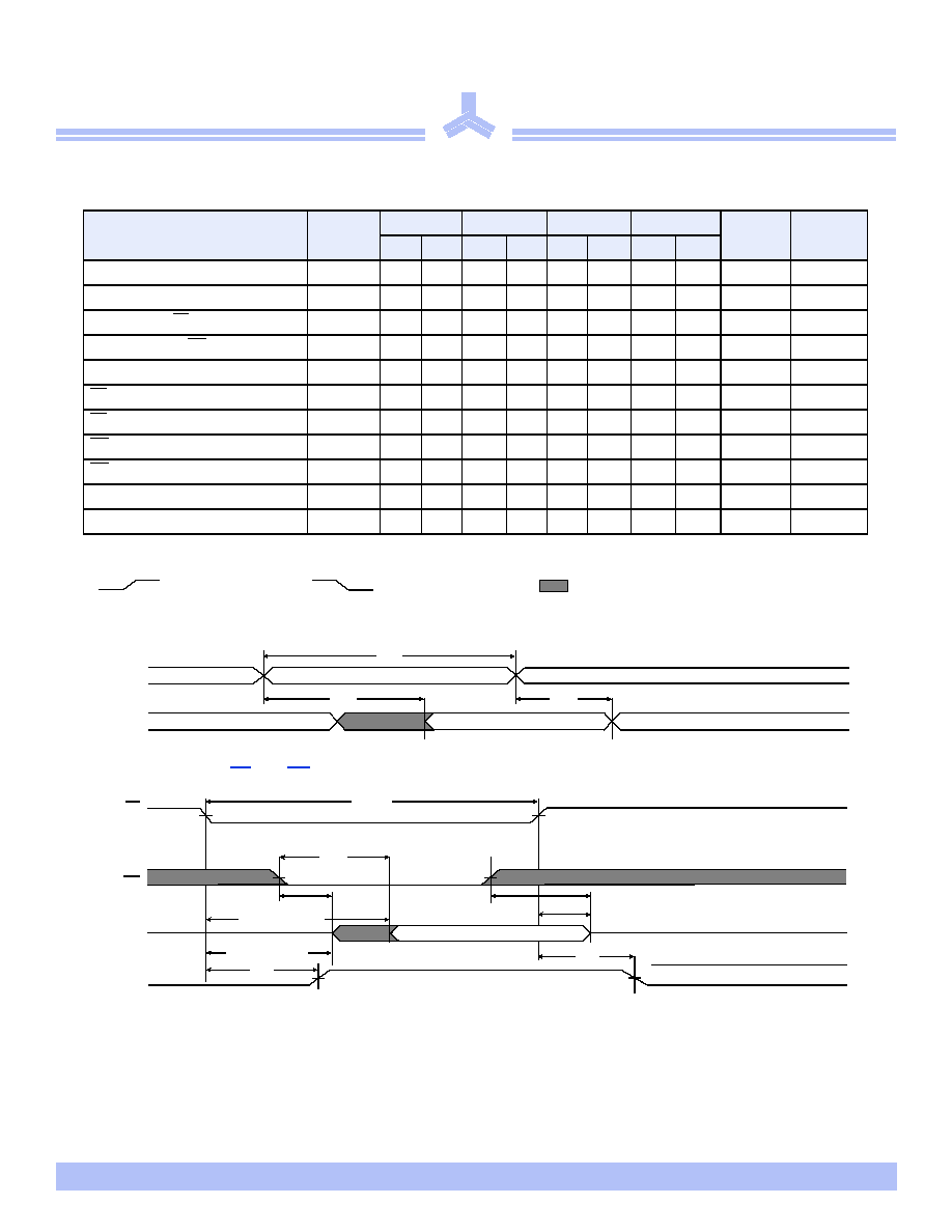
Key to switching waveforms
Read waveform 1 (address controlled)
Read waveform 2 (CE and OE controlled)
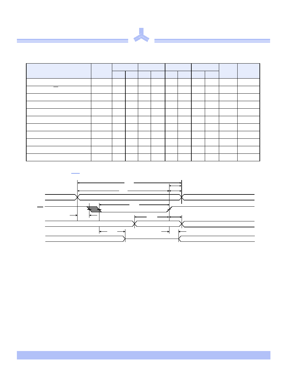
Read cycle (over the operating range)
Parameter
Symbol
-10
-12
-15
-20
Unit
Notes
Min
Max
Min
Max Min
Max
Min
Max
Read cycle time
t
RC
10
≠
12
≠
15
≠
20
≠
ns
Address access time
t
AA
≠
10
≠
12
≠
15
≠
20
ns
3
Chip enable (CE) access time
t
ACE
≠
10
≠
12
≠
15
≠
20
ns
3
Output enable (OE) access time
t
OE
≠
5
≠
6
≠
7
≠
8
ns
Output hold from address change
t
OH
2
≠
3
≠
3
≠
3
≠
ns
5
CE
/RZ W
o output in low Z
t
CLZ
0
≠
0
≠
0
≠
0
≠
ns
4, 5
CE Low to output in high Z
t
CHZ
≠
3
≠
3
≠
4
≠
5
ns
4, 5
OE Low to output in low Z
t
OLZ
0
≠
0
≠
0
≠
0
≠
ns
4, 5
OE High to output in high Z
t
OHZ
≠
3
≠
3
≠
4
≠
5
ns
4, 5
Power up time
t
PU
0
≠
0
≠
0
≠
0
≠
ns
4, 5
Power down time
t
PD
≠
10
≠
12
≠
15
≠
20
ns
4, 5
Undefined/don't care
Falling input
Rising input
Address
D
OUT
Data valid
t
OH
t
AA
t
RC
current
Supply
OE
D
OUT
t
OE
t
OLZ
t
ACE
t
CHZ
t
CLZ
t
PU
t
PD
I
CC
I
SB
50%
50%
Data valid
t
RC1
CE
t
OHZ
AS7C1025A
AS7C31025A
9/26/02; v.0.9.8
Alliance Semiconductor
P. 5 of 8
Æ
Write waveform 1 (WE controlled)
Write cycle (over the operating range)
Parameter
Symbol
-10
-12
-15
-20
Unit
Notes
Min
Max
Min
Max
Min
Max
Min
Max
Write cycle time
t
WC
10
≠
12
≠
15
≠
20
≠
ns
Chip enable (CE) to write end
t
CW
8
≠
10
≠
12
≠
12
≠
ns
Address setup to write end
t
AW
8
≠
9
≠
10
≠
12
≠
ns
Address setup time
t
AS
0
≠
0
≠
0
≠
0
≠
ns
Write pulse width
t
WP
7
≠
8
≠
9
≠
12
≠
ns
Write recovery time
t
WR
0
≠
0
≠
0
≠
0
≠
ns
Address hold from end of write
t
AH
0
≠
0
≠
0
≠
0
≠
ns
Data valid to write end
t
DW
5
≠
6
≠
8
≠
10
≠
ns
Data hold time
t
DH
0
≠
0
≠
0
≠
0
≠
ns
4, 5
Write enable to output in high Z
t
WZ
≠
6
≠
6
≠
6
≠
8
ns
4, 5
Output active from write end
t
OW
1
≠
1
≠
1
≠
2
≠
ns
4, 5
t
AW
t
AH
t
WC
Address
WE
D
OUT
t
DH
t
OW
t
DW
t
WZ
t
WP
t
AS
Data valid
D
IN
t
WR