0D\
&RS\ULJKW $OOLDQFH 6HPLFRQGXFWRU $OO ULJKWV UHVHUYHG
$6&
Y
$OOLDQFH 6HPLFRQGXFWRU
RI
9 .[ &026 65$0
)HDWXUHV
∑ AS7C164 (5V version)
∑ Commercial temperature
∑ Organization: 8,192 words ◊ 8 bits
∑ Center power and ground pins
∑ High speed
- 12/15/20 ns address access time
- 6/7/8 ns output enable access time
∑ Low power consumption: ACTIVE
- 550 mW (AS7C164) / max @ 12 ns
∑ Low power consumption: STANDBY
- 11 mW (AS7C164) / max CMOS I/O
∑ 2.0V data retention
∑ Easy memory expansion with CE1, CE2, OE inputs
∑ TTL-compatible, three-state I/O
∑ 28-pin JEDEC standard package
- 300 mil SOJ
∑ ESD protection
2000 volts
∑ Latch-up current
200 mA
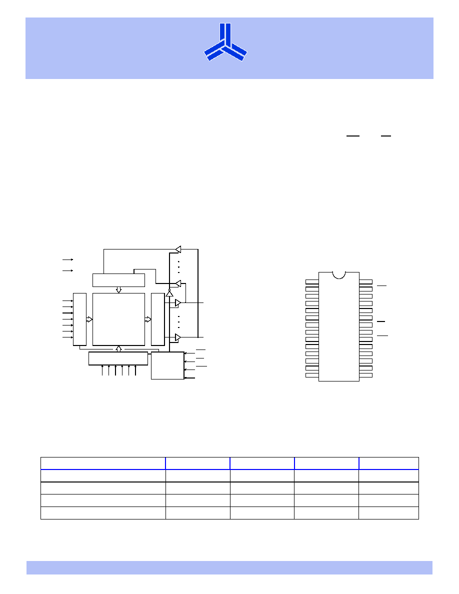
/RJLF EORFN GLDJUDP
A
5
A
0
128◊64◊8
Array
(65,536)
Input buffer
A1
A2
A3
A4
A10
A11
A12
A
6
A
7
A
8
A
9
I/O0
I/O7
V
CC
GND
OE
CE1
WE
Column decoder
R
o
w decoder
Control
circuit
Sense amp
CE2
3LQ DUUDQJHPHQW
1
2
3
4
5
6
7
8
9
10
11
12
13
14
28
27
26
25
24
23
22
21
20
19
18
17
Vcc
WE
CE2
A8
A9
A11
OE
A10
CE1
I/O7
I/O6
I/O5
I/O4
I/O3
NC
A12
A7
A6
A5
A4
A3
A2
A1
A0
I/O0
I/O1
I/O2
GND
28-pin PDIP, SOJ (300 mL)
16
15
AS7
C
16
4
6HOHFWLRQ JXLGH
-12
-15
-20
Unit
Maximum address access time
12
15
20
ns
Maximum output enable access time
6
7
8
ns
Maximum operating current
110
100
90
mA
Maximum CMOS standby current
2.0
2.0
2.0
mA

$6&
Y
$OOLDQFH 6HPLFRQGXFWRU
RI
)XQFWLRQDO GHVFULSWLRQ
The AS7C164 is a high performance CMOS 65,536-bit Static Random Access Memory (SRAM) device organized as 8,192 words ◊ 8 bits. It is
designed for memory applications where fast data access, low power, and simple interfacing are desired.
Equal address access and cycle times (t
AA
, t
RC
, t
WC
) of 12/15/20 ns with output enable access times (t
OE
) of 6/7/8 ns are ideal for high
performance applications. Active high and low chip enables (CE1, CE2) permit easy memory expansion with multiple-bank memory systems.
When CE1 is High or CE2 is Low the device enters standby mode. The standard AS7C164 is guaranteed not to exceed 11.0 mW power
consumption in standby mode, and typically requires only 250 µW; it offers 2.0V data retention with maximum power of 120 µW.
A write cycle is accomplished by asserting write enable (WE) and both chip enables (CE1, CE2). Data on the input pins I/O0-I/O7 is written
on the rising edge of WE (write cycle 1) or the active-to-inactive edge of CE1 or CE2 (write cycle 2). To avoid bus contention, external devices
should drive I/O pins only after outputs have been disabled with output enable (OE) or write enable (WE).
A read cycle is accomplished by asserting output enable (OE) and both chip enables (CE1, CE2), with write enable (WE) High. The chip drives
I/O pins with the data word referenced by the input address. When either chip enable or output enable is inactive, or write enable is active,
output drivers stay in high-impedance mode.
All chip inputs and outputs are TTL-compatible, and operation is from a single 5V supply. The AS7C164 is packaged in 300 mil SOJ packages.
$EVROXWH PD[LPXP UDWLQJV
NOTE: Stresses greater than those listed under Absolute Maximum Ratings may cause permanent damage to the device. This is a stress rating only and functional oper-
ation of the device at these or any other conditions outside those indicated in the operational sections of this specification is not implied. Exposure to absolute
maximum rating conditions for extended periods may affect reliability.
7UXWK WDEOH
Key: X = Don't Care, L = Low, H = High
Parameter
Device
Symbol
Min
Max
Unit
Voltage on V
CC
relative to GND
AS7C164
V
t1
≠0.50
+7.0
V
Voltage on any pin relative to GND
V
t2
≠0.50
V
CC
+ 0.50
V
Power dissipation
P
D
≠
1.0
W
Storage temperature (plastic)
T
stg
≠65
+150
o
C
Ambient temperature with V
CC
applied
T
bias
≠55
+125
o
C
DC current into outputs (low)
I
out
≠
20
mA
CE1
CE2
WE
OE
Data
Mode
H
X
X
X
High Z
Standby (I
SB
, I
SB1
)
X
L
X
X
High Z
Standby (I
SB
, I
SB1
)
L
H
H
H
High Z
Output disable (I
CC
)
L
H
H
L
D
out
Read (I
CC
)
L
H
L
X
D
in
Write (I
CC
)

$6&
Y
$OOLDQFH 6HPLFRQGXFWRU
RI
5HFRPPHQGHG RSHUDWLQJ FRQGLWLRQV
'& RSHUDWLQJ FKDUDFWHULVWLFV RYHU WKH RSHUDWLQJ UDQJH�
&DSDFLWDQFH I 0+] 7
D
R
& 9
&&
120,1$/�
Parameter
Device
Symbol
Min
Typical
Max
Unit
Supply voltage
AS7C164
V
CC
4.5
5.0
5.5
V
Input voltage
AS7C164
V
IH
2.2
≠
V
CC
+1
V
V
IL
≠0.5
*
* V
IL
min = ≠3.0V for pulse width less than t
RC
/2.
≠
0.8
V
Ambient operating temperature
AS7C164
T
A
0
≠
70
o
C
Parameter
Symbol
Test Conditions
Device
-12
-15
-20
Unit
Min Max Min Max Min Max
Input leakage current
|
I
LI
|
V
CC
= Max,
V
IN
= GND to V
CC
≠
1
≠
1
≠
1
µA
Output leakage current
|
I
LO
|
V
CC
= Max,
CE1 = V
IH
or CE2 = V
IL
,
V
OUT
= GND to V
CC
≠
1
≠
1
≠
1
µA
Operating power supply
current
I
CC
V
CC
= Max,
CE1 = V
IL
, CE2 = V
IH
,
f = f
Max,
I
OUT
= 0 mA
AS7C164
≠
110
≠
100
≠
90
mA
Standby power supply
current
I
SB
V
CC
= Max,
CE1 = V
IH
or CE2 = V
IL
,
f = f
Max
AS7C164
≠
30
≠
25
≠
25
mA
I
SB1
V
CC
= Max,
CE1
V
CC
≠0.2V or
CE2
0.2V,
V
IN
0.2V or
V
IN
V
CC
≠0.2V, f = 0
AS7C164
≠
2.0
≠
2.0
≠
2.0
mA
Output voltage
V
OL
I
OL
= 8 mA, V
CC
= Min
≠
0.4
≠
0.4
≠
0.4
V
V
OH
I
OH
= ≠4 mA, V
CC
= Min
2.4
≠
2.4
≠
2.4
≠
V
Parameter
Symbol
Signals
Test conditions
Max
Unit
Input capacitance
C
IN
A, CE1, CE2, WE, OE
V
in
= 0V
5
pF
I/O capacitance
C
I/O
I/O
V
in
= V
out
= 0V
7
pF

$6&
Y
$OOLDQFH 6HPLFRQGXFWRU
RI
5HDG F\FOH RYHU WKH RSHUDWLQJ UDQJH�
.H\ WR VZLWFKLQJ ZDYHIRUPV
5HDG ZDYHIRUP DGGUHVV FRQWUROOHG�
5HDG ZDYHIRUP &( DQG &( FRQWUROOHG�
Parameter
Symbol
-12
-15
-20
Unit
Notes
Min
Max
Min
Max
Min
Max
Read cycle time
t
RC
12
≠
15
≠
20
≠
ns
Address access time
t
AA
≠
12
≠
15
≠
20
ns
3
Chip enable (CE1) access time
t
ACE1
≠
12
≠
15
≠
20
ns
3, 12
Chip enable (CE2) access time
t
ACE2
≠
12
≠
15
≠
20
ns
3, 12
Output enable (OE) access time
t
OE
≠
6
≠
7
≠
8
ns
Output hold from address change
t
OH
3
≠
3
≠
3
≠
ns
5
CE1 Low to output in low Z
t
CLZ1
3
≠
3
≠
3
≠
ns
4, 5, 12
CE2 High to output in low Z
t
CLZ2
3
≠
3
≠
3
≠
ns
4, 5, 12
CE1 High to output in high Z
t
CHZ1
≠
3
≠
4
≠
5
ns
4, 5, 12
CE2 Low to output in high Z
t
CHZ2
≠
3
≠
4
≠
5
ns
4, 5, 12
OE Low to output in low Z
t
OLZ
0
≠
0
≠
0
≠
ns
4, 5
OE High to output in high Z
t
OHZ
≠
3
≠
4
≠
5
ns
4, 5
Power up time
t
PU
0
≠
0
≠
0
≠
ns
4, 5, 12
Power down time
t
PD
≠
12
≠
15
≠
20
ns
4, 5, 12
Undefined/don't care
Falling input
Rising input
Address
D
OUT
Data valid
t
OH
t
AA
t
RC
current
Supply
CE2
OE
D
OUT
t
OE
t
OLZ
t
ACE1,
t
ACE2
t
CHZ1,
t
CHZ2
t
CLZ1,
t
CLZ2
t
PU
t
PD
I
CC
I
SB
50%
50%
t
OHZ
Data valid
t
RC
1
CE1

$6&
Y
$OOLDQFH 6HPLFRQGXFWRU
RI
:ULWH F\FOH RYHU WKH RSHUDWLQJ UDQJH�
:ULWH ZDYHIRUP :( FRQWUROOHG�
:ULWH ZDYHIRUP &( DQG &( FRQWUROOHG�
Parameter
Symbol
-12
-15
-20
Unit
Notes
Min
Max
Min
Max
Min
Max
Write cycle time
t
WC
12
≠
15
≠
20
≠
ns
Chip enable (CE1) to write end
t
CW1
9
≠
10
≠
12
≠
ns
12
Chip enable (CE2) to write end
t
CW2
9
≠
10
≠
12
≠
ns
12
Address setup to write end
t
AW
9
≠
10
≠
12
≠
ns
Address setup time
t
AS
0
≠
0
≠
0
≠
ns
12
Write pulse width
t
WP
8
≠
9
≠
12
≠
ns
Write recovery time
t
WR
0
≠
0
≠
0
≠
ns
Address hold from write end
t
AH
0
≠
0
≠
0
≠
ns
Data valid to write end
t
DW
6
≠
7
≠
8
≠
ns
Data hold time
t
DH
0
≠
0
≠
0
≠
ns
4, 5
Write enable to output in high Z
t
WZ
≠
5
≠
5
≠
5
ns
4, 5
Output active from write end
t
OW
3
≠
3
≠
3
≠
ns
4, 5
t
AW
t
AH
t
WC
Address
WE
D
OUT
t
DH
t
OW
t
DW
t
WZ
t
WP
t
AS
Data valid
D
IN
t
WR
t
AW
Address
CE1
WE
D
OUT
t
CW1,
t
CW2
t
WP
t
DW
t
DH
t
AH
t
WZ
t
WC
t
AS
CE2
Data valid
D
IN
t
WR

$6&
Y
$OOLDQFH 6HPLFRQGXFWRU
RI
'DWD UHWHQWLRQ FKDUDFWHULVWLFV RYHU WKH RSHUDWLQJ UDQJH�
'DWD UHWHQWLRQ ZDYHIRUP
$& WHVW FRQGLWLRQV
1RWHV
1
During V
CC
power-up, a pull-up resistor to V
CC
on CE1 is required to meet I
SB
specification.
2
This parameter is sampled, but not 100% tested.
3
For test conditions, see AC Test Conditions, Figures A, B, and C.
4
t
CLZ
and t
CHZ
are specified with CL = 5pF as in Figures B or C. Transition is measured
±
500mV from steady-state voltage.
5
This parameter is guaranteed, but not 100% tested.
6
WE is High for read cycle.
7
CE1 and OE are Low and CE2 is High for read cycle.
8
Address valid prior to or coincident with CE1 transition Low and CE2 transition High.
9
All read cycle timings are referenced from the last valid address to the first transitioning address.
10 CE1 or WE must be High or CE2 Low during address transitions. Either CE or WE asserting high terminates a write cycle.
11 All write cycle timings are referenced from the last valid address to the first transitioning address.
12 CE1 and CE2 have identical timing.
13 2V data retention applies to the commercial operating range only.
14 C = 30pF, except on High Z and Low Z parameters, where C = 5pF.
Parameter
Symbol
Test conditions
Min
Max
Unit
V
CC
for data retention
V
DR
V
CC
= 2.0V
CE1
V
CC
≠0.2V or
CE2
0.2V
2.0
≠
V
Data retention current
I
CCDR
≠
60
µA
Chip enable to data retention time
t
CDR
0
≠
ns
Operation recovery time
t
R
t
RC
≠
ns
V
CC
CE1
t
R
t
CDR
Data retention mode
V
CC
V
CC
V
DR
2.0V
V
IH
V
IH
V
DR
CS2
t
R
t
CDR
V
IH
V
IH
V
DR
- Output load: see Figure B or Figure C.
- Input pulse level: GND to 3.0V. See Figure A.
- Input rise and fall times: 2 ns. See Figure A.
- Input and output timing reference levels: 1.5V.
10%
90%
10%
90%
GND
+3.0V
Figure A: Input pulse
2ns
255
C
(14)
480
D
RXW
GND
+5V
Figure B: 5V Output lo
DG
255
C
(14)
320
D
RXW
GND
+5V
Figure C: 3.3V Output load
168
Thevenin Equivalent:
D
RXW
+1.728V (5V)

$6&
Y
$OOLDQFH 6HPLFRQGXFWRU
RI
7\SLFDO '& DQG $& FKDUDFWHULVWLFV
Supply voltage (V)
MIN
MAX
NOMINAL
0.0
0.2
0.6
0.8
0.4
1.0
1.2
1.4
No
r
m
a
l
iz
ed
I
CC
, I
SB
Normalized supply current I
CC
, I
SB
Ambient temperature (∞C)
≠55
80
125
35
≠10
0.0
0.2
0.6
0.8
0.4
1.0
1.2
1.4
No
r
m
a
l
iz
ed
I
CC
, I
SB
Normalized supply current I
CC
, I
SB
vs. ambient temperature T
a
vs. supply voltage V
CC
I
CC
I
SB
I
CC
I
SB
Ambient temperature (∞C)
-55
80
125
35
-10
0.2
1
0.04
5
25
625
No
r
m
al
ized
I
SB1
(
l
o
g
s
c
a
l
e)
Normalized supply current I
SB1
vs. ambient temperature T
a
V
CC
= V
CC
(NOMINAL)
Supply voltage (V)
MIN
MAX
NOMINAL
0.8
0.9
1.1
1.2
1.0
1.3
1.4
1.5
Nor
m
alized acc
ess time
Normalized access time t
AA
Ambient temperature (∞C)
≠55
80
125
35
≠10
0.8
0.9
1.1
1.2
1.0
1.3
1.4
1.5
Nor
m
alized acc
ess time
Normalized access time t
AA
Cycle frequency (MHz)
0
75
100
50
25
0.0
0.2
0.6
0.8
0.4
1.0
1.2
1.4
No
r
m
ali
z
ed
I
CC
Normalized supply current I
CC
vs. ambient temperature T
a
vs. cycle frequency 1/t
RC
, 1/t
WC
vs. supply voltage V
CC
V
CC
= V
CC
(NOMINAL)
T
a
= 25∞C
V
CC
= V
CC
(NOMINAL)
T
a
= 25∞C
Output voltage (V)
V
CC
0
20
60
80
40
100
120
140
Output source cur
r
ent (mA)
Output source current I
OH
Output voltage (V)
V
CC
Output sink cur
r
e
n
t (mA)
Output sink current I
OL
vs. output voltage V
OL
vs. output voltage V
OH
0
20
60
80
40
100
120
140
V
CC
= V
CC
(NOMINAL)PL
T
a
= 25∞C
V
CC
= V
CC
(NOMINAL)
T
a
= 25∞C
Capacitance (pF)
0
750
1000
500
250
0
5
15
20
10
25
30
35
Change in t
AA
(ns)
Typical access time change
t
AA
vs. output capacitive loading
V
CC
= V
CC
(NOMINAL)
0
0

$6&
Y
$OOLDQFH 6HPLFRQGXFWRU
RI
© Copyright Alliance Semiconductor Corporation. All rights reserved. Our three-point logo, our name and Intelliwatt are trademarks or registered trademarks of Alliance. All other brand and product names may be the trademarks
of their respective companies. Alliance reserves the right to make changes to this document and its products at any time without notice. Alliance assumes no responsibility for any errors that may appear in this document. The data
contained herein represents Alliance's best data and/or estimates at the time of issuance. Alliance reserves the right to change or correct this data at any time, without notice. If the product described herein is under development,
significant changes to these specifications are possible. The information in this product data sheet is intended to be general descriptive information for potential customers and users, and is not intended to operate as, or provide,
any guarantee or warrantee to any user or customer. Alliance does not assume any responsibility or liability arising out of the application or use of any product described herein, and disclaims any express or implied warranties
related to the sale and/or use of Alliance products including liability or warranties related to fitness for a particular purpose, merchantability, or infringement of any intellectual property rights, except as express agreed to in
Alliance's Terms and Conditions of Sale (which are available from Alliance). All sales of Alliance products are made exclusively according to Alliance's Terms and Conditions of Sale. The purchase of products from Alliance does not
convey a license under any patent rights, copyrights, mask works rights, trademarks, or any other intellectual property rights of Alliance or third parties. Alliance does not authorize its products for use as critical components in
life-supporting systems where a malfunction or failure may reasonably be expected to result in significant injury to the user, and the inclusion of Alliance products in such life-supporting systems implies that the manufacturer
assumes all risk of such use and agrees to indemnify Alliance against all claims arising from such use
3DFNDJH GLPHQVLRQV
2UGHULQJ FRGHV
3DUW QXPEHULQJ V\VWHP
Package\
Access time
Volt/Temp
12 ns
15 ns
20 ns
Plastic SOJ\300 mL
5V commercial
AS7C164-12JC
AS7C164-15JC
AS7C164-20JC
AS7C
164
X
≠XX
X
C
SRAM prefix
Device number
Blank = Standard power
Access time
Package code:
J=SOJ 300 mil
Commercial
temperature range,
0∞C to 70∞C
28-pin SOJ in mil
Min
Max
A
-
0.140
A1
0.025
-
A2
0.095
0.105
B
0.028 TYP
b
0.018 TYP
c
0.010 TYP
D
-
0.730
E
0.245
0.285
E1
0.295
0.305
E2
0.327
0.347
e
0.050 BSC
H
'
(
3LQ
E
%
$
$
F
(
Seating
Plane
(
$
300 mil 28-pin SOJ