Äîêóìåíòàöèÿ è îïèñàíèÿ www.docs.chipfind.ru

September 2005
ASM5P23S08A
rev 1.4
Alliance Semiconductor
2575 Augustine Drive
· Santa Clara, CA · Tel: 408.855.4900 · Fax: 408.855.4999 · www.alsc.com
Notice: The information in this document is subject to change without notice.
3.3V `SpreadTrak' Zero Delay Buffer
General Features
·
Zero input - output propagation delay, adjustable by
capacitive load on FBK input.
· Multiple configurations - Refer "ASM5P23S08A
Configurations" Table.
·
Input frequency range: 15MHz to 133MHz
· Multiple
low-skew
outputs.
o Output-output skew less than 200pS.
o Device-device skew less than 700pS.
o Two banks of four outputs, three-stateable by two
select inputs.
·
Less than 200pS Cycle-to-cycle jitter
(-1, -1H, -2, -3, -4, -5H).
·
Available in 16 pin SOIC and TSSOP Packages.
· 3.3V
operation.
·
Advanced 0.35µ CMOS technology.
·
Industrial temperature available.
· `SpreadTrak'.
Functional Description
ASM5P23S08A is a versatile, 3.3V zero-delay buffer
designed to distribute high-speed clocks. It is available in a
16 pin package. The part has an on-chip PLL, which locks
to an input clock, presented on the REF pin. The PLL
feedback is required to be driven to FBK pin, and can be
obtained from one of the outputs. The input-to-output
propagation delay is guaranteed to be less than 250pS,
and the output-to-output skew is guaranteed to be less than
200pS.
The ASM5P23S08A has two banks of four outputs each,
which can be controlled by the select inputs as shown in
the Select Input Decoding Table. The select input also
allows the input clock to be directly applied to the outputs
for chip and system testing purposes.
Multiple ASM5P23S08A devices can accept the same input
clock and distribute it. In this case the skew between the
outputs of the two devices is guaranteed to be less than
700pS.
The ASM5P23S08A is available in five different
configurations (Refer "ASM5P23S08A Configurations
Table). The ASM5P23S08A-1 is the base part, where the
output frequencies equal the reference if there is no
counter in the feedback path. The ASM5P23S08A-1H is
the high-drive version of the -1 and the rise and fall times
on this device are faster.
The ASM5P23S08A-2 allows the user to obtain 2X and 1X
frequencies on each output bank. The exact configuration
and output frequencies depends on which output drives the
feedback pin. The ASM5P23S08A-3 allows the user to
obtain 4X and 2X frequencies on the outputs.
The ASM5P23S08A-4 enables the user to obtain 2X clocks
on all outputs. Thus, the part is extremely versatile, and
can be used in a variety of applications.
The ASM5P23S08A-5H is a high-drive version with REF/2
on both banks
September 2005
ASM5P23S08A
rev 1.4
3.3V `SpreadTrak' Zero Delay Buffer
2 of 18
Notice: The information in this document is subject to change without notice.
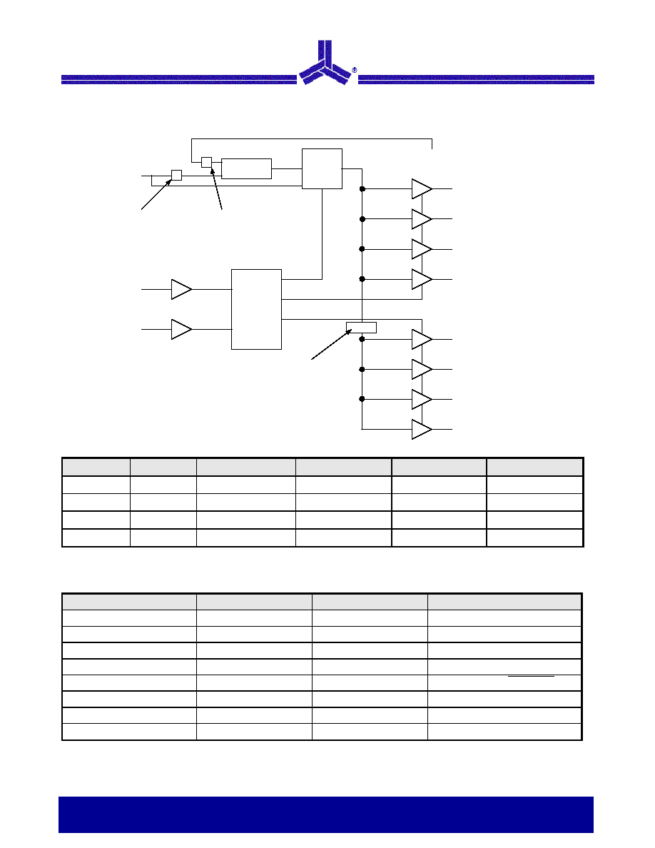
Block Diagram
Select Input Decoding for ASM5P23S08A
S2
S1
Clock A1 - A4
Clock B1 - B4
Output Source
PLL Shut-Down
0 0
Three-state
Three-state PLL
Y
0 1 Driven Three-state PLL
N
1 0 Driven
1
Driven
Reference Y
1 1 Driven Driven
PLL
N
ASM5P23S08A Configurations
Device
Feedback From
Bank A Frequency
Bank B Frequency
ASM5P23S08A-1
Bank A or Bank B
Reference
Reference
ASM5P23S08A-1H
Bank A or Bank B
Reference
Reference
ASM5P23S08A-2
Bank A
Reference
Reference /2
ASM5P23S08A-2
Bank B
2 X Reference
Reference
ASM5P23S08A-3
Bank A
2 X Reference
Reference or Reference
2
ASM5P23S08A-3
Bank B
4 X Reference
2 X Reference
ASM5P23S08A-4
Bank A or Bank B
2 X Reference
2 X Reference
ASM5P23S08A-5H
Bank A or Bank B
Reference /2
Reference /2
Note:
1. Outputs are non- inverted on ASM5P23S08A-2 and ASM5P23S08A-3 in bypass mode, S2 = 1 and S1 = 0.
2. Output phase is indeterminant (0° or 180° from input clock). If phase integrity is required, use the ASM5P23S08A-2.
/2
MUX
Select Input
Decoding
CLKA1
CLKA2
CLKA3
CLKA4
CLKB1
CLKB2
CLKB3
CLKB4
Extra Divider (-2, -3)
PLL
/2
/2
Extra Divider (-3, -4)
Extra Divider (-5H)
REF
S2
S1
FBK
ASM5P23S08A
September 2005
ASM5P23S08A
rev 1.4
Notice: The information in this document is subject to change without notice.
3.3V `SpreadTrak' Zero Delay Buffer
3 of 18
`SpreadTrak'
Many systems being designed now utilize a technology
called Spread Spectrum Frequency Timing Generation.
ASM5P23S08A is designed so as not to filter off the
Spread Spectrum feature of the Reference input, assuming
it exists. When a zero delay buffer is not designed to pass
the Spread Spectrum feature through, the result is a
significant amount of tracking skew which may cause
problems in the systems requiring synchronization.
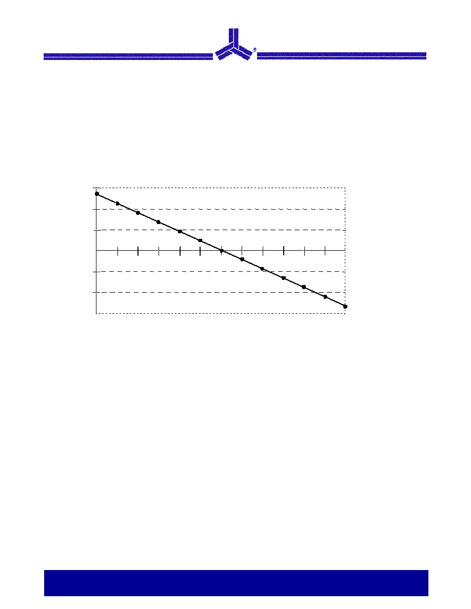
Zero Delay and Skew Control
All outputs should be uniformly loaded to achieve Zero
Delay between input and output.
To close the feedback loop of the ASM5P23S08A, the FBK
pin can be driven from any of the eight available output
pins. The output driving the FBK pin will be driving a total
load of 7pF plus any additional load that it drives. The
relative loading of this output (with respect to the remaining
outputs) can adjust the input output delay. This is shown in
the above graph.
For applications requiring zero input-output delay, all
outputs including the one providing feedback should be
equally loaded. If input-output delay adjustments are
required, use the above graph to calculate loading
differences between the feedback output and remaining
outputs. For zero output-output skew, make sure to load
outputs equally.
-30
-25
-20
-15
-10
-5
0
5
10
15
20
25
30
0
-500
-1000
-1500
500
1000
1500
Output Load Difference: FBK Load - CLKA/CLKB Load (pF)
R
E
F
-
In
p
u
t
to
C
L
KA
/L
K
B
D
e
la
y (
p
S)
September 2005
ASM5P23S08A
rev 1.4
3.3V `SpreadTrak' Zero Delay Buffer
4 of 18
Notice: The information in this document is subject to change without notice.
Pin Configuration
Pin Description for ASM5P23S08A
Pin #
Pin Name
Description
1 REF
3
Input reference frequency, 5V tolerant input
2 CLKA1
4
Buffered clock output, bank A
3 CLKA2
4
Buffered clock output, bank A
4 V
DD
3.3V
supply
5 GND
Ground
6 CLKB1
4
Buffered clock output, bank B
7 CLKB2
4
Buffered clock output, bank B
8 S2
5
Select input, bit 2
9 S1
5
Select input, bit 1
10 CLKB3
4
Buffered clock output, bank B
11 CLKB4
4
Buffered clock output, bank B
12 GND
Ground
13 V
DD
3.3V
supply
14 CLKA3
4
Buffered clock output, bank A
15 CLKA4
4
Buffered clock output, bank A
16
FBK
PLL feedback input
Notes:
3. Weak pull-down.
4. Weak pull-down on all outputs.
5. Weak pull-up on these inputs.
11
9
10
12
13
14
15
16
S2
2
1
3
4
5
6
7
8
V
DD
CLKA3
CLKB3
CLKB4
FBK
V
DD
GND
CLKB1
S1
CLKA1
REF
CLKB2
CLKA4
CLKA2
GND
ASM5P23S08A
September 2005
ASM5P23S08A
rev 1.4
3.3V `SpreadTrak' Zero Delay Buffer
5 of 18
Notice: The information in this document is subject to change without notice.
Absolute Maximum Ratings
Parameter
Min
Max
Unit
Supply Voltage to Ground Potential
-0.5
+7.0
V
DC Input Voltage (Except REF)
-0.5
V
DD
+ 0.5
V
DC Input Voltage (REF)
-0.5
7
V
Storage Temperature
-65
+150
°C
Max. Soldering Temperature (10 sec)
260
°C
Junction Temperature
150
°C
Static Discharge Voltage
(As per JEDEC STD22- A114-B)
2000
V
Note: These are stress ratings only and functional usage is not implied. Exposure to absolute maximum ratings for prolonged periods can
affect device reliability.
Operating Conditions for ASM5P23S08A Commercial Temperature Devices
Parameter
Description
Min
Max
Unit
V
DD
Supply
Voltage
3.0
3.6
V
T
A
Operating Temperature (Ambient Temperature)
0
70
°C
C
L
Load Capacitance, below 100MHz
30
pF
C
L
Load Capacitance, from 100MHz to 133MHz
15
pF
C
IN
Input
Capacitance
6
7
pF
Note:
6. Applies to both Ref Clock and FBK.