Äîêóìåíòàöèÿ è îïèñàíèÿ www.docs.chipfind.ru
September 2005
ASM5P2304A
rev 1.4
Notice: The information in this document is subject to change without notice.
Alliance Semiconductor
2575 Augustine Drive
·
Santa Clara, CA
·
Tel: 408.855.4900
·
Fax: 408.855.4999
·
www.alsc.com
3.3V Zero Delay Buffer
Features
Zero input - output propagation delay, adjustable
by capacitive load on FBK input.
Multiple configurations - Refer "ASM5P2304A
Configurations Table".
Input frequency range: 15MHz to 133MHz
Multiple low-skew outputs.
Output-output skew less than 200pS.
Device-device skew less than 500pS.
Two banks of four outputs.
Less than 200pS Cycle-to-Cycle jitter
(-1, -1H, -2, -2H).
Available in space saving, 8 pin 150-mil SOIC
packages.
3.3V operation.
Advanced 0.35< CMOS technology.
Industrial temperature available.
Functional Description
ASM5P2304A is a versatile, 3.3V zero-delay buffer
designed to distribute high-speed clocks in PC,
workstation, datacom, telecom and other high-performance
applications. It is available in 8 pin package. The part has
an on-chip PLL which locks to an input clock presented on
the REF pin. The PLL feedback is required to be driven to
FBK pin, and can be obtained from one of the outputs. The
input-to-output propagation delay is guaranteed to be less
than 250pS, and the output-to-output skew is guaranteed to
be less than 200pS.
The ASM5P2304A has two banks of two outputs each.
Multiple ASM5P2304A devices can accept the same input
clock and distribute it. In this case the skew between the
outputs of the two devices is guaranteed to be less than
500pS.
The ASM5P2304A is available in two different
configurations (Refer "ASM5P2304A Configurations Table).
The ASM5P2304A-1 is the base part, where the output
frequencies equal the reference if there is no counter in the
feedback path. The ASM5P2304A-1H is the high-drive
version of the -1 and the rise and fall times on this device
are much faster.
The ASM5P2304A-2 allows the user to obtain REF and
1/2X or 2X frequencies on each output bank. The exact
configuration and output frequencies depend on which
output drives the feedback pin.
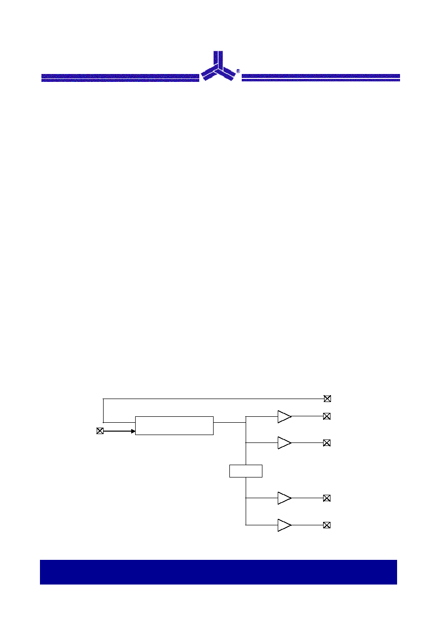
Block Diagram
PLL
/2
Extra Divider (-2)
CLKA2
CLKA1
FBK
CLKB1
CLKB2
REF
September 2005
ASM5P2304A
rev 1.4
3.3V Zero Delay Buffer
2 of 15
Notice: The information in this document is subject to change without notice.
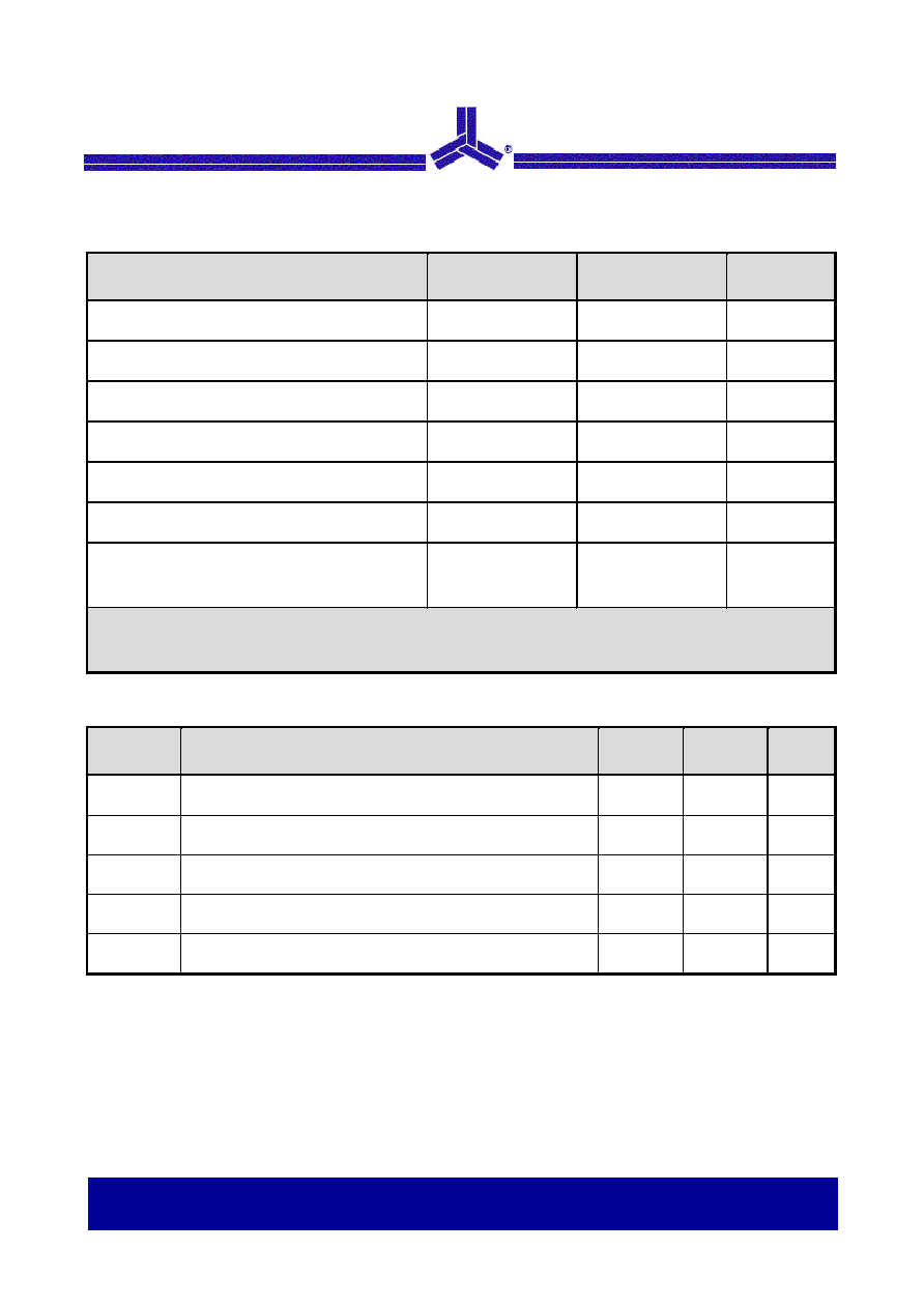
ASM5P2304A Configurations
Device
Feedback From
Bank A Frequency
Bank B Frequency
ASM5P2304A-1
Bank A or Bank B
Reference
Reference
ASM5P2304A-1H
Bank A or Bank B
Reference
Reference
ASM5P2304A-2
Bank A
Reference
Reference /2
ASM5P2304A-2
Bank B
2 X Reference
Reference
ASM5P2304A-2H Bank
A
Reference Reference/2
ASM5P2304A-2H
Bank B
2 X Reference
Reference
Zero Delay and Skew Control
For applications requiring zero input-output delay, all outputs must be equally loaded
.
To close the feedback loop of the ASM5P2304A, the FBK
pin can be driven from any of the four available output pins.
The output driving the FBK pin will be driving a total load of
7pF plus any additional load that it drives. The relative
loading of this output (with respect to the remaining
outputs) can adjust the input output delay. This is shown in
the above graph.
For applications requiring zero input-output delay, all
outputs including the one providing feedback should be
equally loaded. If input-output delay adjustments are
required, use the above graph to calculate loading
differences between the feedback output and remaining
outputs. For zero output-output skew, be sure to load
outputs equally.
-30
-25
-20
-15
-10
-5
0
5
10
15
20
25
30
0
-500
-1000
-1500
500
1000
1500
Output Load Difference: FBK Load - CLKA/CLKB Load (pF)
R
E
F
-
I
n
p
u
t
t
o
C
L
K
A
/
C
L
K
B
D
e
l
a
y
(
p
S
)
REF Input to CLKA/CLKB Delay Vs Difference in Loading between FBK pin and CLKA/CLKB pins

September 2005
ASM5P2304A
rev 1.4
3.3V Zero Delay Buffer
3 of 15
Notice: The information in this document is subject to change without notice.
Pin Configuration
Pin Description for ASM5P2304A
Pin #
Pin Name
Description
1
REF
1
Input reference frequency, 5V tolerant input
2
CLKA1
2
Buffered clock output, bank A
3
CLKA2
2
Buffered clock output, bank A
4
GND Ground
5
CLKB1
2
Buffered clock output, bank B
6
CLKB2
2
Buffered clock output, bank B
7
V
DD
3.3V
supply
8
FBK
PLL feedback input
Notes:
1. Weak pull-down.
2. Weak pull-down on all outputs.
ASM5P2304A
5
6
7
8 FBK
V
DD
CLKB2
CLKB1
4
3
2
1
GND
CLKA1
REF
CLKA2
September 2005
ASM5P2304A
rev 1.4
3.3V Zero Delay Buffer
4 of 15
Notice: The information in this document is subject to change without notice.
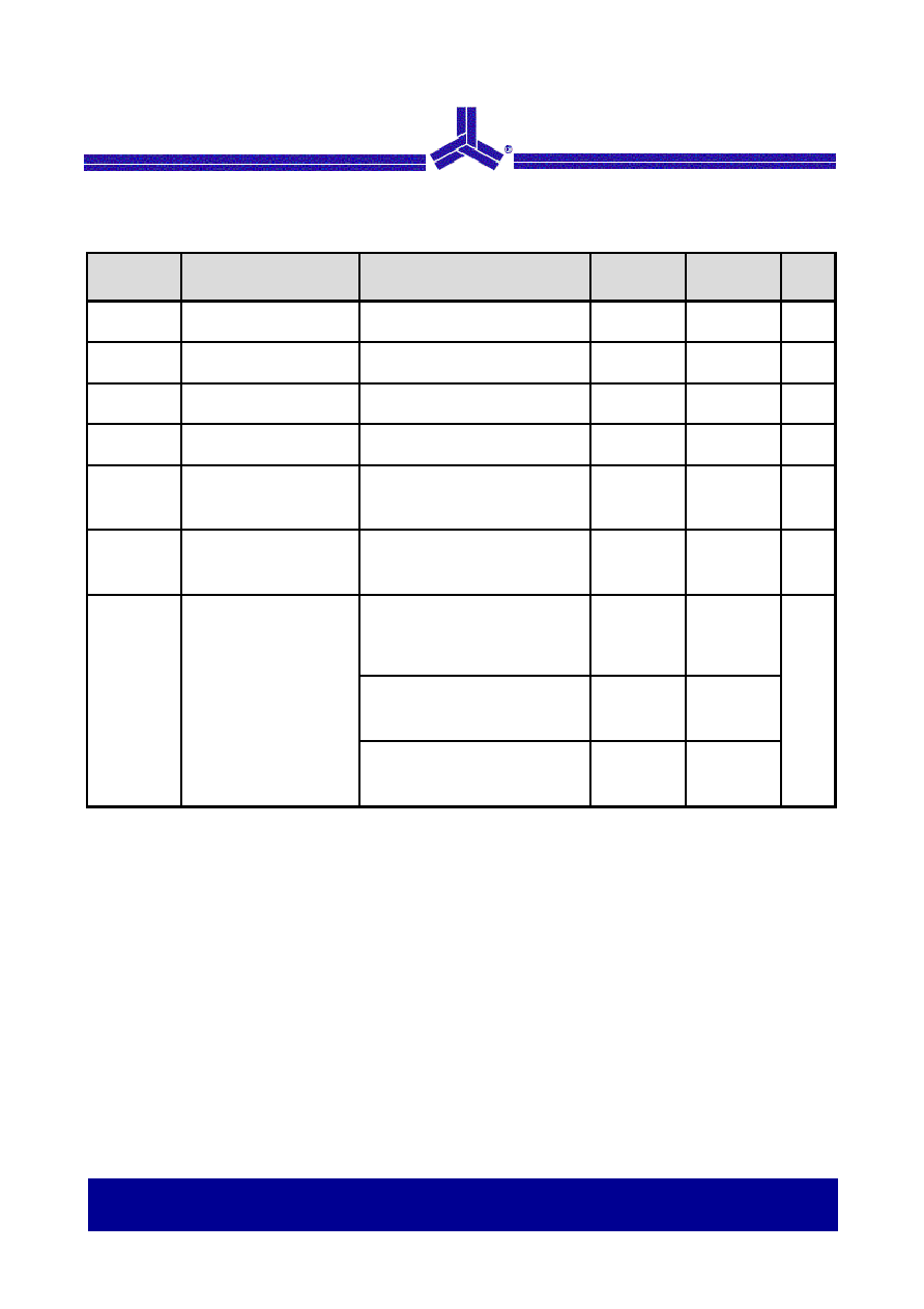
Absolute Maximum Ratings
Parameter
Min
Max
Unit
Supply Voltage to Ground Potential
-0.5
+7.0
V
DC Input Voltage (Except REF)
-0.5
V
DD
+ 0.5
V
DC Input Voltage (REF)
-0.5
7
V
Storage Temperature
-65
+150
°C
Max. Soldering Temperature (10 sec)
260
°C
Junction Temperature
150
°C
Static Discharge Voltage
(As per JEDEC STD22- A114-B)
2000
V
Note: These are stress ratings only and functional usage is not implied. Exposure to absolute maximum ratings for prolonged periods can affect device
reliability.
Operating Conditions for ASM5P2304A Commercial Temperature Devices
Parameter
Description
Min
Max
Unit
V
DD
Supply
Voltage
3.0
3.6
V
T
A
Operating Temperature (Ambient Temperature)
0
70
°C
C
L
Load Capacitance, from 15MHz to 100MHz
30
pF
C
L
Load Capacitance, from 100MHz to 133MHz
15
pF
C
IN
Input
Capacitance
3
7
pF
Note:
3. Applies to both Ref Clock and FBK.
September 2005
ASM5P2304A
rev 1.4
3.3V Zero Delay Buffer
5 of 15
Notice: The information in this document is subject to change without notice.
Electrical Characteristics for ASM5P2304A Commercial Temperature Devices
Parameter
Description
Test Conditions
Min
Max
Unit
V
IL
Input
LOW
Voltage
0.8 V
V
IH
Input HIGH Voltage
2.0
V
I
IL
Input
LOW
Current V
IN
= 0V
50.0
<A
I
IH
Input
HIGH
Current V
IN
= V
DD
100.0
<A
V
OL
Output
LOW
Voltage
4
I
OL
= 8mA (-1, -2)
I
OH
= 12mA (-1H, -2H)
0.4
V
V
OH
Output
HIGH
Voltage
4
I
OL
= -8mA (-1, -2)
I
OH
= -12mA (-1H, -2H)
2.4
V
Unloaded outputs 100MHz REF,
Select inputs at V
DD
or GND
45.0
Unloaded outputs, 66MHz REF
(-1, -1H, -2, -2H)
32.0
I
DD
Supply
Current
Unloaded outputs, 33MHz REF
(-1, -1H, -2, -2H)
18.0
mA
Note:
4. Parameter is guaranteed by design and characterization. Not 100% tested in production.