October 2003
P1817A/B
rev 1.0
Alliance Semiconductor
2575, Augustine Drive
∑ Santa Clara, CA ∑ Tel: 408.855.4900 ∑ Fax: 408.855.4999 ∑ www.alsc.com
Notice: The information in this document is subject to change without notice.
Low-Power Mobile VGA EMI Reduction IC
Features
FCC approved method of EMI attenuation.
Generates a low EMI spread spectrum clock of the
input frequency.
Optimized for frequency range from:
o
P1817A ≠ 20 to 30MHz. Operation
o
P1817B ≠ 10 to 20MHz Operation
Internal loop filter minimizes external components
and board space.
Two selectable spread ranges.
Low inherent cycle-to-cycle jitter.
3.3V or 5V operating voltage range.
TTL or CMOS compatible outputs.
Ultra-low power CMOS design.
3.17mA @3.3V, 10MHz | 6.20mA@5.0V, 10MHz
4.28mA @3.3V, 14MHz | 7.50mA @5.0V, 14MHz
5.50mA @3.3V, 20MHz | 9.50mA @5.0V, 20MHz
Supports notebook VGA and other LCD timing
controller applications.
SSON pin for Spread Spectrum On/Off and
Standby Mode controls.
Available in 8-pin SOIC and TSSOP.
Product Description
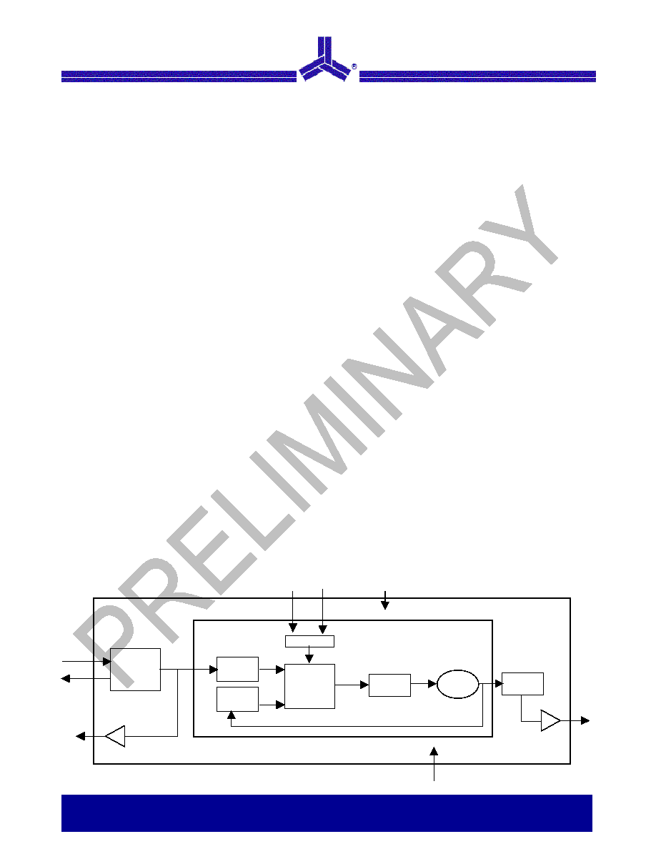
The P1817 is a versatile spread spectrum frequency
modulator designed specifically for input clock frequencies.
The P1817 reduces electromagnetic interference (EMI) at
the clock source, allowing system wide reduction of EMI of
down stream clock and data dependent signals. The P1817
allows significant system cost savings by reducing the
number of circuit board layers ferrite beads, shielding and
other passive components that are traditionally required to
pass EMI regulations.
The P1817 modulates the output of a single PLL in order to
"spread" the bandwidth of a synthesized clock, and more
importantly, decreases the peak amplitudes of its
harmonics. This results in significantly lower system EMI
compared to the typical narrow band signal produced by
oscillators and most frequency generators. Lowering EMI
by increasing a signal's bandwidth is called `spread
spectrum clock generation'.
The P1817 uses the most efficient and optimized
modulation profile approved by the FCC and is
implemented in a proprietary all digital method.
Applications
The P1817 is targeted towards notebook VGA chip and
other displays using an LVDS interface, PC peripheral
devices, and embedded systems.
Block Diagram
VSS
XIN
XOUT
Crystal
Oscillator
Frequency
Divider
Feedback
Divider
Modulation
Phase
Detector
Loop
Filter
VCO
Output
Divider
ModOUT
PLL
VDD
SSON
SR0
Ref

October 2003
P1817A/B
rev 1.0
Low Frequency EMI Reduction
2 of 10
Notice: The information in this document is subject to change without notice.
ModOUT
1
2
3
4
5
6
7
8
P1817A/B
XIN /CLKIN
VSS
SR0
SSON/SBM
REF
VDD
XOUT
Pin Configuration
Pin Description
Pin#
Pin Name
Type
Description
1 XIN/CLKIN I
Connect to externally generated clock signal. To put the part into standby
mode, disable the input clock signal to this pin and pull SSON/SBM (pin 4)
low. Refer Standby Mode Selection Table.
2
VSS
P
Ground Connection. Connect to system ground.
3 SR0 I
Digital logic input used to select Spreading Range. Refer Spread Spectrum
Selection Table. This pin has an internal pull-up resistor.
4 SSON/SBM I
Spread Spectrum On/Off and standby mode control. Refer Standby Mode
Selection Table.
5 ModOUT O
Spread spectrum clock output or reference output. Refer Standby Mode
Selection Table.
6 REF O
Reference
output.
7
VDD
P
Connect to +3.3V or 5.0V.
8
XOUT
O
Connect to crystal. No connect if externally generated clock signal is used.
October 2003
P1817A/B
rev 1.0
Low Frequency EMI Reduction
3 of 10
Notice: The information in this document is subject to change without notice.
Standby Mode Selection
CLKIN
SSON/SBM
Spread
Spectrum
ModOUT
PLL
Mode
Disabled 0 N/A Disabled
Disabled
Standby
Disabled
1
N/A
Disabled
Free Running
Free Running
Enabled 0
Off
Reference
Disabled
Buffer
out
Enabled 1
On Normal Normal Normal
Spread Range Selection, VDD = 5V
CLKIN frequency
SR0
Spreading Range
Modulation Rate
1 ±
1.5%
10 MHz
0 ±
1.9%
1 ±
1.36%
14.318MHz
0 ±
1.64%
1 ±
1.3%
15MHz
0 ±
1.5%
1 ±
0.95%
20MHz
0 ±
1.125%
(CLKIN/10) * 20.83KHz
Spread Range Selection, VDD = 3.3V
CLKIN frequency
SR0
Spreading Range
Modulation Rate
1 ±
1.5%
10 MHz
0 ±
1.65%
1 ±
1.4%
14.318MHz
0 ±
1.7%
1 ±
1.37%
15MHz
0 ±
1.63%
1 ±
1.1%
20MHz
0 ±
1.28%
(CLKIN/10) * 20.83KHz

October 2003
P1817A/B
rev 1.0
Low Frequency EMI Reduction
4 of 10
Notice: The information in this document is subject to change without notice.
Schematic for Notebook VGA Application
1
. To set the P1817 to standby mode, disable the input clock (pin 1 CLKIN), and pull pin 4 SSON/SBM low.
VDD
1
VDD
VDD
2
3
4
5
6
7
8
Ferrite
Bead
0.1µF
0
0
0
0
CLKIN/
XIN
VSS
SR0
SSON/
SBM
ModOUT
REF
VDD
XOUT
Use either pull-up or pull-down
resistors with 0.
Pull pin 4 low to turn Spread Spectrum
off and enable Standby Mode
1
.
10 to 20 MHz and 20 to 32 MHz EMI
reduced clock output.
P1817A/B
October 2003
P1817A/B
rev 1.0
Low Frequency EMI Reduction
5 of 10
Notice: The information in this document is subject to change without notice.
Absolute Maximum Ratings
Symbol
Parameter
Rating
Unit
V
DD
, V
IN
Voltage on any pin with respect to GND
-0.5 to + 7.0
V
T
STG
Storage
temperature
-65 to +125
∞C
T
A
Operating
temperature
0 to 70
∞C
Note: These are stress ratings only and functional operation is not implied. Exposure to absolute maximum
ratings for extended periods may affect device reliability.
DC Electrical Characteristics
Symbol
Parameter
Min
Typ
Max
Unit
V
IL
Input low voltage
GND ≠ 0.3
-
0.8
V
V
IH
Input high voltage
2.0
-
V
DD
+ 0.3
V
I
IL
Input low current (pull-up resistors on inputs SR0 and
SSON/SBM)
- -
-35
µA
I
IH
Input high current (pull-down resistor on input SSON#)
-
-
35
µA
@ 0.4V, V
DD
= 3.3V
-
3
-
I
XOL
X
OUT
output low current
@ 0.4V, V
DD
= 5.0V
-
20
-
mA
@ 2.5V, V
DD
= 3.3V
-
3
-
I
XOH
X
OUT
output high current
@ 4.5V, V
DD
= 5.0V
-
20
-
mA
V
DD
=3.3V, I
OL
= 20mA
-
-
0.4
V
OL
Output low voltage
V
DD
=5.0V, I
OL
= 20mA
-
-
-
V
V
DD
=3.3V, I
O
H
= 20mA
2.5
-
-
V
OH
Output high voltage
V
DD
=5.0V, I
O
H
= 20mA
4.5
-
-
V
Normal Mode
f
IN-min
f
IN-typ
f
IN-max
3.3V and 10pF loading
3.2
-
7.0
I
CC
Dynamic supply current
normal mode
5.0V and 10pF loading
6.2
-
13.6
mA
I
DD
Static supply current standby mode
-
0.6
-
mA
V
DD
Operating
voltage
2.7 3.3 5.5 V
t
ON
Power up time (first locked clock cycle after power up)
-
0.18
-
mS
Z
OUT
Clock output impedance
-
50
-