
Æ
Altera Corporation
1
Stratix GX
FPGA Family
March 2003, ver. 1.2
Data Sheet
DS-STXGX-1.2
Introduction
Preliminary
Information
The Stratix
TM
GX family of devices is Altera's second FPGA family to
combine high-speed serial transceivers with a scalable, high-performance
logic array. Stratix GX devices include 4 to 20 high-speed transceiver
channels, each incorporating clock data recovery (CDR) technology and
embedded SERDES capability at data rates of up to 3.125 gigabits per
second (Gbps). These transceivers are grouped in integrated, four-channel
blocks, and are designed for low power consumption and small die size.
The Stratix GX FPGA technology is built upon the Stratix architecture,
and offers a 1.5-V logic array with unmatched performance, flexibility,
and time-to-market capabilities. This scalable, high-performance
architecture makes Stratix GX devices ideal for high-speed backplane
interface, chip-to-chip, and communications protocol-bridging
applications.
Features...
Transceiver block features
≠
High-speed serial transceiver channels with CDR provides
622-megabits per second (Mbps) to 3.125-Gbps full-duplex
transceiver operation per channel
≠
Devices available with 4, 8, 16, or 20 high-speed serial transceiver
channels providing up to 62.5 Gbps of serial bandwidth (full-
duplex)
≠
Support for transceiver-based protocols, including 10 Gigabit
Ethernet XAUI, SONET/SDH, 1 Gigabit Ethernet, PCI Express,
SMPTE 292M, SFI-5, SPI-5, InfiniBand, Fibre Channel, and Serial
RapidIO
≠
Programmable differential output voltage (V
OD
) and pre-
emphasis settings for improved signal integrity
≠
Individual transmitter and receiver channel power-down
capability for reduced power consumption during non-
operation
≠
Selectable on-chip termination resistors (50
, 60
, or 75
) for
improved signal integrity on a variety of transmission media
≠
Programmable transceiver-to-FPGA interface with support for
8-, 10-, 16-, and 20-bit wide data transfer
≠
1.5-V pseudo current mode logic (PCML) for 622 Mbps to
3.125 Gbps (both AC and DC coupling)
≠
Receiver indicator for loss of signal
≠
Built-in self test (BIST)
≠
Hot insertion/removal protection circuitry
≠
Pattern detector and word aligner supports programmable
patterns

2
Altera Corporation
Stratix GX FPGA Family Data Sheet
Preliminary Information
≠
8B/10B encoder/decoder performs 8-bit to 10-bit encoding and
10-bit to 8-bit decoding
≠
Transceiver synchronizer buffer performs clock domain
translation between the transceiver block and the logic array
≠
Receiver FIFO resynchronizes the received data with the local
reference clock
≠
Rate matcher and channel aligner compliant with XAUI
≠
Device can bypass these transceiver block features if necessary
FPGA features
≠
10,570 to 41,250 logic elements (LEs); see
Table 1
≠
Up to 3,423,744 RAM bits (427,968 bytes) available without
reducing logic resources
≠
TriMatrix
TM
memory consisting of three RAM block sizes to
implement true dual-port memory and first-in first-out (FIFO)
buffers with performance up to 312 MHz
≠
Up to 16 global clock networks with up to 22 regional clock
networks per device region
≠
High-speed DSP blocks provide dedicated implementation of
multipliers (at up to 250 MHz), multiply- accumulate functions,
and finite impulse response (FIR) filters
≠
Up to four enhanced PLLs per device provide spread spectrum,
programmable bandwidth, clock switch-over, real-time PLL
reconfiguration, and advanced multiplication and phase shifting
≠
Support for numerous single-ended and differential I/O
standards
≠
High-speed source-synchronous differential I/O support on up
to 45 channels with up to 40 channels optimized for 1-Gbps
performance
≠
Support for source-synchronous bus standards, including
10-Gigabit Ethernet XSBI, Parallel RapidIO, UTOPIA IV,
Network Packet Streaming Interface (NPSI), HyperTransport
TM
technology, SPI-4 Phase 2 (POS-PHY Level 4), and SFI-4
≠
Terminator
TM
technology provides on-chip termination for
differential and single-ended I/O pins with impedance
matching
≠
Support for high-speed external memory, including zero bus
turnaround (ZBT) SRAM, quad data rate (QDR and QDRII)
SRAM, double data rate (DDR) SDRAM, DDR fast cycle RAM
(FCRAM), and single data rate (SDR) SDRAM
≠
Support for multiple intellectual property megafunctions from
Altera MegaCore
Æ
functions and Altera Megafunction Partners
Program (AMPP
SM
) megafunctions
≠
Support for remote configuration updates
Altera Corporation
3
Preliminary Information
Stratix GX FPGA Family Data Sheet
Note to
Table 1
:
(1)
This parameter lists the total number of 9
◊
9-bit multipliers for each device. For the total number of 18
◊
18-bit
multipliers per device, divide the total number of 9
◊
9-bit multipliers by 2. For the total number of 36
◊
36-bit
multipliers per device, decide the total number of 9
◊
9-bit multipliers by 8.
Stratix GX devices are available in space-saving FineLine BGA
and ball-
grid array (BGA) packages (see
Tables 2
through
3
). All Stratix GX devices
support vertical migration within the same package (e.g., the designer can
migrate between the EP1SGX10C and EP1SGX25C devices in the 672-pin
FineLine BGA package). Vertical migration means that designers can
migrate to devices whose dedicated pins, configuration pins, and power
pins are the same for a given package across device densities. For I/O pin
migration across densities, the designer must cross reference the available
I/O pins using the device pin-outs for all planned densities of a given
package type to identify which I/O pins are migratable. The Quartus
Æ
II
software can automatically cross reference and place all pins except LVDS
pins for migration when given a device migration list. The designer must
use the pin-outs for each device to verify the LVDS placement migration.
A future version of the Quartus II software will support LVDS pin
migration.
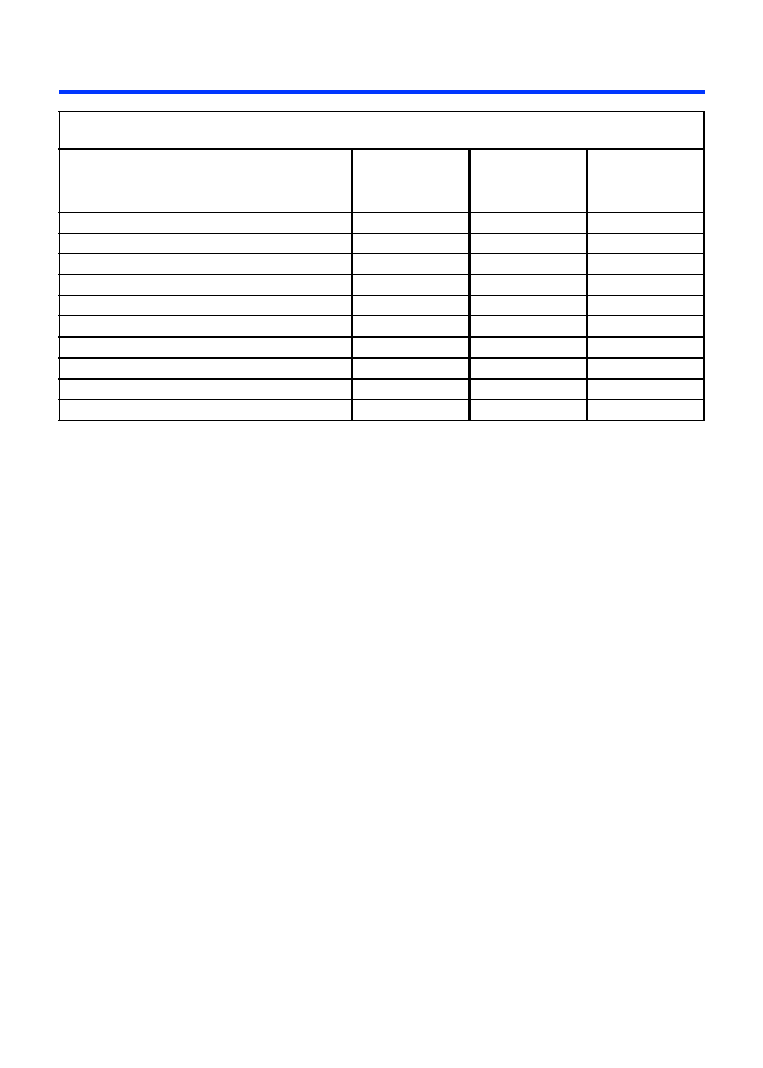
Table 1. Stratix GX Device Features
Feature
EP1SGX10C
EP1SGX10D
EP1SGX25C
EP1SGX25D
EP1SGX25F
EP1SGX40D
EP1SGX40G
LEs
10,570
25,660
41,250
Transceiver channels
4, 8
4, 8, 16
8, 20
Source-synchronous channels
22
39
45
M512 RAM blocks (32
◊
18 bits)
94
224
384
M4K RAM blocks (128
◊
36 bits)
60
138
183
M-RAM blocks (4K
◊
144 bits)
1
2
4
Total RAM bits
920,448
1,944,576
3,423,744
Digital signal processing (DSP) blocks
6
10
14
Embedded multipliers
(1)
48
80
112
PLLs
4
4
8

