 | –≠–ª–µ–∫—Ç—Ä–æ–Ω–Ω—ã–π –∫–æ–º–ø–æ–Ω–µ–Ω—Ç: FLEX10KE | –°–∫–∞—á–∞—Ç—å:  PDF PDF  ZIP ZIP |
Document Outline
- FLEX 10KE Embedded Programmable Logic Device Data Sheet

Altera Corporation
1
FLEX 10KE
Embedded Programmable
Logic Device
January 2003, ver. 2.5
Data Sheet
DS-F10KE-2.5
Æ
Features...
Embedded programmable logic devices (PLDs), providing
system-on-a-programmable-chip (SOPC) integration in a single
device
≠
Enhanced embedded array for implementing megafunctions
such as efficient memory and specialized logic functions
≠
Dual-port capability with up to 16-bit width per embedded array
block (EAB)
≠
Logic array for general logic functions
High density
≠
30,000 to 200,000 typical gates (see
Tables 1
and
2
)
≠
Up to 98,304 RAM bits (4,096 bits per EAB), all of which can be
used without reducing logic capacity
System-level features
≠
MultiVolt
TM
I/O pins can drive or be driven by 2.5-V, 3.3-V, or
5.0-V devices
≠
Low power consumption
≠
Bidirectional I/O performance (t
SU
and t
CO
) up to 212 MHz
≠
Fully compliant with the PCI Special Interest Group (PCI SIG)
PCI Local Bus Specification, Revision 2.2
for 3.3-V operation at
33 MHz or 66 MHz
≠
-1 speed grade devices are compliant with
PCI Local Bus
Specification, Revision 2.2
, for 5.0-V operation
≠
Built-in Joint Test Action Group (JTAG) boundary-scan test
(BST) circuitry compliant with IEEE Std. 1149.1-1990, available
without consuming additional device logic
f
For information on 5.0-V FLEX
Æ
10K or 3.3-V FLEX 10KA devices, see the
FLEX 10K Embedded Programmable Logic Family Data Sheet
.
Table 1. FLEX 10KE Device Features
Feature
EPF10K30E
EPF10K50E
EPF10K50S
Typical gates
(1)
30,000
50,000
Maximum system gates
119,000
199,000
Logic elements (LEs)
1,728
2,880
EABs
6
10
Total RAM bits
24,576
40,960
Maximum user I/O pins
220
254

2
Altera Corporation
FLEX 10KE Embedded Programmable Logic Devices Data Sheet
Note to tables:
(1)
The embedded IEEE Std. 1149.1 JTAG circuitry adds up to 31,250 gates in addition to the listed typical or maximum
system gates.
(2)
New EPF10K100B designs should use EPF10K100E devices.
...and More
Features
≠
Fabricated on an advanced process and operate with a 2.5-V
internal supply voltage
≠
In-circuit reconfigurability (ICR) via external configuration
devices, intelligent controller, or JTAG port
≠
ClockLock
TM
and ClockBoost
TM
options for reduced clock
delay/skew and clock multiplication
≠
Built-in low-skew clock distribution trees
≠
100% functional testing of all devices; test vectors or scan chains
are not required
≠
Pull-up on I/O pins before and during configuration
Flexible interconnect
≠
FastTrack
Æ
Interconnect continuous routing structure for fast,
predictable interconnect delays
≠
Dedicated carry chain that implements arithmetic functions such
as fast adders, counters, and comparators (automatically used by
software tools and megafunctions)
≠
Dedicated cascade chain that implements high-speed,
high-fan-in logic functions (automatically used by software tools
and megafunctions)
≠
Tri-state emulation that implements internal tri-state buses
≠
Up to six global clock signals and four global clear signals
Powerful I/O pins
≠
Individual tri-state output enable control for each pin
≠
Open-drain option on each I/O pin
≠
Programmable output slew-rate control to reduce switching
noise
≠
Clamp to V
CCIO
user-selectable on a pin-by-pin basis
≠
Supports hot-socketing
Table 2. FLEX 10KE Device Features
Feature
EPF10K100E
(2)
EPF10K130E
EPF10K200E
EPF10K200S
Typical gates
(1)
100,000
130,000
200,000
Maximum system gates
257,000
342,000
513,000
Logic elements (LEs)
4,992
6,656
9,984
EABs
12
16
24
Total RAM bits
49,152
65,536
98,304
Maximum user I/O pins
338
413
470

Altera Corporation
3
FLEX 10KE Embedded Programmable Logic Devices Data Sheet
Software design support and automatic place-and-route provided by
Altera's development systems for Windows-based PCs and Sun
SPARCstation, and HP 9000 Series 700/800
Flexible package options
≠
Available in a variety of packages with 144 to 672 pins, including
the innovative FineLine BGA
TM
packages (see
Tables 3
and
4
)
≠
SameFrame
TM
pin-out compatibility between FLEX 10KA and
FLEX 10KE devices across a range of device densities and pin
counts
Additional design entry and simulation support provided by EDIF
2 0 0 and 3 0 0 netlist files, library of parameterized modules (LPM),
DesignWare components, Verilog HDL, VHDL, and other interfaces
to popular EDA tools from manufacturers such as Cadence,
Exemplar Logic, Mentor Graphics, OrCAD, Synopsys, Synplicity,
VeriBest, and Viewlogic
Notes:
(1)
FLEX 10KE device package types include thin quad flat pack (TQFP), plastic quad flat pack (PQFP), power quad flat
pack (RQFP), pin-grid array (PGA), and ball-grid array (BGA) packages.
(2)
Devices in the same package are pin-compatible, although some devices have more I/O pins than others. When
planning device migration, use the I/O pins that are common to all devices.
(3)
This option is supported with a 484-pin FineLine BGA package. By using SameFrame pin migration, all
FineLine BGA packages are pin-compatible. For example, a board can be designed to support 256-pin, 484-pin, and
672-pin FineLine BGA packages. The Altera software automatically avoids conflicting pins when future migration
is set.
Table 3. FLEX 10KE Package Options & I/O Pin Count
Notes (1)
,
(2)
Device
144-Pin
TQFP
208-Pin
PQFP
240-Pin
PQFP
RQFP
256-Pin
FineLine
BGA
356-Pin
BGA
484-Pin
FineLine
BGA
599-Pin
PGA
600-Pin
BGA
672-Pin
FineLine
BGA
EPF10K30E
102
147
176
220
220
(3)
EPF10K50E
102
147
189
191
254
254
(3)
EPF10K50S
102
147
189
191
220
254
254
(3)
EPF10K100E
147
189
191
274
338
338
(3)
EPF10K130E
186
274
369
424
413
EPF10K200E
470
470
470
EPF10K200S
182
274
369
470
470
470

4
Altera Corporation
FLEX 10KE Embedded Programmable Logic Devices Data Sheet
General
Description
Altera FLEX 10KE devices are enhanced versions of FLEX 10K devices.
Based on reconfigurable CMOS SRAM elements, the FLEX architecture
incorporates all features necessary to implement common gate array
megafunctions. With up to 200,000 typical gates, FLEX 10KE devices
provide the density, speed, and features to integrate entire systems,
including multiple 32-bit buses, into a single device.
The ability to reconfigure FLEX 10KE devices enables 100
%
testing prior
to shipment and allows the designer to focus on simulation and design
verification. FLEX 10KE reconfigurability eliminates inventory
management for gate array designs and generation of test vectors for fault
coverage.
Table 5
shows FLEX 10KE performance for some common designs. All
performance values were obtained with Synopsys DesignWare or LPM
functions. Special design techniques are not required to implement the
applications; the designer simply infers or instantiates a function in a
Verilog HDL, VHDL, Altera Hardware Description Language (AHDL), or
schematic design file.
Table 4. FLEX 10KE Package Sizes
Device
144-
Pin
TQFP
208-Pin
PQFP
240-Pin
PQFP
RQFP
256-Pin
FineLine
BGA
356-
Pin
BGA
484-Pin
FineLine
BGA
599-Pin
PGA
600-
Pin
BGA
672-Pin
FineLine
BGA
Pitch (mm)
0.50
0.50
0.50
1.0
1.27
1.0
≠
1.27
1.0
Area (mm
2
)
484
936
1,197
289
1,225
529
3,904
2,025
729
Length
◊
width
(mm
◊
mm)
22
◊
22 30.6
◊
30.6 34.6
◊
34.6
17
◊
17
35
◊
35
23
◊
23
62.5
◊
62.5 45
◊
45
27
◊
27

Altera Corporation
5
FLEX 10KE Embedded Programmable Logic Devices Data Sheet
Notes:
(1)
This application uses combinatorial inputs and outputs.
(2)
This application uses registered inputs and outputs.
Table 6
shows FLEX 10KE performance for more complex designs. These
designs are available as Altera MegaCore
Æ
functions.
Note:
(1)
These values are for calculation time. Calculation time = number of clocks required/f
max
. Number of clocks
required = ceiling [log 2 (points)/2]
◊
[points +14 + ceiling]
Table 5. FLEX 10KE Performance
Application
Resources Used
Performance
Units
LEs
EABs
-1 Speed Grade -2 Speed Grade -3 Speed Grade
16-bit loadable counter
16
0
285
250
200
MHz
16-bit accumulator
16
0
285
250
200
MHz
16-to-1 multiplexer
(1)
10
0
3.5
4.9
7.0
ns
16-bit multiplier with 3-stage
pipeline
(2)
592
0
156
131
93
MHz
256
◊
16 RAM read cycle
speed
(2)
0
1
196
154
118
MHz
256
◊
16 RAM write cycle
speed
(2)
0
1
185
143
106
MHz
Table 6. FLEX 10KE Performance for Complex Designs
Application
LEs Used
Performance
Units
-1 Speed Grade -2 Speed Grade -3 Speed Grade
8-bit, 16-tap parallel finite impulse
response (FIR) filter
597
192
156
116
MSPS
8-bit, 512-point fast Fourier
transform (FFT) function
1,854
23.4
28.7
38.9
µ
s
(1)
113
92
68
MHz
a16450
universal asynchronous
receiver/transmitter (UART)
342
36
28
20.5 MHz

6
Altera Corporation
FLEX 10KE Embedded Programmable Logic Devices Data Sheet
Similar to the FLEX 10KE architecture, embedded gate arrays are the
fastest-growing segment of the gate array market. As with standard gate
arrays, embedded gate arrays implement general logic in a conventional
"sea-of-gates" architecture. Additionally, embedded gate arrays have
dedicated die areas for implementing large, specialized functions. By
embedding functions in silicon, embedded gate arrays reduce die area
and increase speed when compared to standard gate arrays. While
embedded megafunctions typically cannot be customized, FLEX 10KE
devices are programmable, providing the designer with full control over
embedded megafunctions and general logic, while facilitating iterative
design changes during debugging.
Each FLEX 10KE device contains an embedded array and a logic array.
The embedded array is used to implement a variety of memory functions
or complex logic functions, such as digital signal processing (DSP), wide
data-path manipulation, microcontroller applications, and data-
transformation functions. The logic array performs the same function as
the sea-of-gates in the gate array and is used to implement general logic
such as counters, adders, state machines, and multiplexers. The
combination of embedded and logic arrays provides the high
performance and high density of embedded gate arrays, enabling
designers to implement an entire system on a single device.
FLEX 10KE devices are configured at system power-up with data stored
in an Altera serial configuration device or provided by a system
controller. Altera offers the EPC1, EPC2, and EPC16 configuration
devices, which configure FLEX 10KE devices via a serial data stream.
Configuration data can also be downloaded from system RAM or via the
Altera BitBlaster
TM
, ByteBlasterMV
TM
, or MasterBlaster download cables.
After a FLEX 10KE device has been configured, it can be reconfigured
in-circuit by resetting the device and loading new data. Because
reconfiguration requires less than 85 ms, real-time changes can be made
during system operation.
FLEX 10KE devices contain an interface that permits microprocessors to
configure FLEX 10KE devices serially or in-parallel, and synchronously or
asynchronously. The interface also enables microprocessors to treat a
FLEX 10KE device as memory and configure it by writing to a virtual
memory location, making it easy to reconfigure the device.

Altera Corporation
7
FLEX 10KE Embedded Programmable Logic Devices Data Sheet
f
For more information on FLEX device configuration, see the following
documents:
Configuration Devices for APEX & FLEX Devices Data Sheet
BitBlaster Serial Download Cable Data Sheet
ByteBlasterMV Parallel Port Download Cable Data Sheet
MasterBlaster Download Cable Data Sheet
Application Note 116 (Configuring APEX 20K, FLEX 10K, & FLEX 6000
Devices)
FLEX 10KE devices are supported by the Altera development systems,
which are integrated packages that offer schematic, text (including
AHDL), and waveform design entry, compilation and logic synthesis, full
simulation and worst-case timing analysis, and device configuration. The
Altera software provides EDIF 2 0 0 and 3 0 0, LPM, VHDL, Verilog HDL,
and other interfaces for additional design entry and simulation support
from other industry-standard PC- and UNIX workstation-based EDA
tools.
The Altera software works easily with common gate array EDA tools for
synthesis and simulation. For example, the Altera software can generate
Verilog HDL files for simulation with tools such as Cadence Verilog-XL.
Additionally, the Altera software contains EDA libraries that use device-
specific features such as carry chains, which are used for fast counter and
arithmetic functions. For instance, the Synopsys Design Compiler library
supplied with the Altera development system includes DesignWare
functions that are optimized for the FLEX 10KE architecture.
The Altera development system runs on Windows-based PCs and Sun
SPARCstation, and HP 9000 Series 700/800.
f
See the MAX+
PLUS II Programmable Logic Development System & Software
Data Sheet
and the
Quartus Programmable Logic Development System &
Software Data Sheet
for more information.

8
Altera Corporation
FLEX 10KE Embedded Programmable Logic Devices Data Sheet
Functional
Description
Each FLEX 10KE device contains an enhanced embedded array to
implement memory and specialized logic functions, and a logic array to
implement general logic.
The embedded array consists of a series of EABs. When implementing
memory functions, each EAB provides 4,096 bits, which can be used to
create RAM, ROM, dual-port RAM, or first-in first-out (FIFO) functions.
When implementing logic, each EAB can contribute 100 to 600 gates
towards complex logic functions, such as multipliers, microcontrollers,
state machines, and DSP functions. EABs can be used independently, or
multiple EABs can be combined to implement larger functions.
The logic array consists of logic array blocks (LABs). Each LAB contains
eight LEs and a local interconnect. An LE consists of a four-input look-up
table (LUT), a programmable flipflop, and dedicated signal paths for carry
and cascade functions. The eight LEs can be used to create medium-sized
blocks of logic--such as 8-bit counters, address decoders, or state
machines--or combined across LABs to create larger logic blocks. Each
LAB represents about 96 usable gates of logic.
Signal interconnections within FLEX 10KE devices (as well as to and from
device pins) are provided by the FastTrack Interconnect routing structure,
which is a series of fast, continuous row and column channels that run the
entire length and width of the device.
Each I/O pin is fed by an I/O element (IOE) located at the end of each row
and column of the FastTrack Interconnect routing structure. Each IOE
contains a bidirectional I/O buffer and a flipflop that can be used as either
an output or input register to feed input, output, or bidirectional signals.
When used with a dedicated clock pin, these registers provide exceptional
performance. As inputs, they provide setup times as low as 0.9 ns and
hold times of 0 ns. As outputs, these registers provide clock-to-output
times as low as 3.0 ns. IOEs provide a variety of features, such as JTAG
BST support, slew-rate control, tri-state buffers, and open-drain outputs.

Altera Corporation
9
FLEX 10KE Embedded Programmable Logic Devices Data Sheet
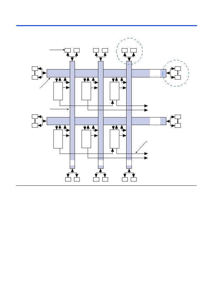
Figure 1
shows a block diagram of the FLEX 10KE architecture. Each
group of LEs is combined into an LAB; groups of LABs are arranged into
rows and columns. Each row also contains a single EAB. The LABs and
EABs are interconnected by the FastTrack Interconnect routing structure.
IOEs are located at the end of each row and column of the FastTrack
Interconnect routing structure.
Figure 1. FLEX 10KE Device Block Diagram
FLEX 10KE devices provide six dedicated inputs that drive the flipflops'
control inputs and ensure the efficient distribution of high-speed, low-
skew (less than 1.5 ns) control signals. These signals use dedicated routing
channels that provide shorter delays and lower skews than the FastTrack
Interconnect routing structure. Four of the dedicated inputs drive four
global signals. These four global signals can also be driven by internal
logic, providing an ideal solution for a clock divider or an internally
generated asynchronous clear signal that clears many registers in the
device.
I/O Element
(IOE)
Logic Array
Block (LAB)
Row
Interconnect
IOE
IOE
IOE
IOE
IOE
IOE
IOE
Local Interconnect
IOE
IOE
IOE
IOE
IOE
IOE
IOE
IOE
IOE
IOE
Logic Element (LE)
Column
Interconnect
IOE
EAB
EAB
Logic
Array
IOE
IOE
IOE
IOE
IOE
IOE
Embedded Array Block (EAB)
Embedded Array
IOE
IOE
Logic Array
IOE
IOE

10
Altera Corporation
FLEX 10KE Embedded Programmable Logic Devices Data Sheet
Embedded Array Block
The EAB is a flexible block of RAM, with registers on the input and output
ports, that is used to implement common gate array megafunctions.
Because it is large and flexible, the EAB is suitable for functions such as
multipliers, vector scalars, and error correction circuits. These functions
can be combined in applications such as digital filters and
microcontrollers.
Logic functions are implemented by programming the EAB with a read-
only pattern during configuration, thereby creating a large LUT. With
LUTs, combinatorial functions are implemented by looking up the results,
rather than by computing them. This implementation of combinatorial
functions can be faster than using algorithms implemented in general
logic, a performance advantage that is further enhanced by the fast access
times of EABs. The large capacity of EABs enables designers to implement
complex functions in one logic level without the routing delays associated
with linked LEs or field-programmable gate array (FPGA) RAM blocks.
For example, a single EAB can implement any function with 8 inputs and
16 outputs. Parameterized functions such as LPM functions can take
advantage of the EAB automatically.
The FLEX 10KE EAB provides advantages over FPGAs, which implement
on-board RAM as arrays of small, distributed RAM blocks. These small
FPGA RAM blocks must be connected together to make RAM blocks of
manageable size. The RAM blocks are connected together using
multiplexers implemented with more logic blocks. These extra
multiplexers cause extra delay, which slows down the RAM block. FPGA
RAM blocks are also prone to routing problems because small blocks of
RAM must be connected together to make larger blocks. In contrast, EABs
can be used to implement large, dedicated blocks of RAM that eliminate
these timing and routing concerns.
The FLEX 10KE enhanced EAB adds dual-port capability to the existing
EAB structure. The dual-port structure is ideal for FIFO buffers with one
or two clocks. The FLEX 10KE EAB can also support up to 16-bit-wide
RAM blocks and is backward-compatible with any design containing
FLEX 10K EABs. The FLEX 10KE EAB can act in dual-port or single-port
mode. When in dual-port mode, separate clocks may be used for EAB read
and write sections, which allows the EAB to be written and read at
different rates. It also has separate synchronous clock enable signals for
the EAB read and write sections, which allow independent control of
these sections.
Altera Corporation
11
FLEX 10KE Embedded Programmable Logic Devices Data Sheet
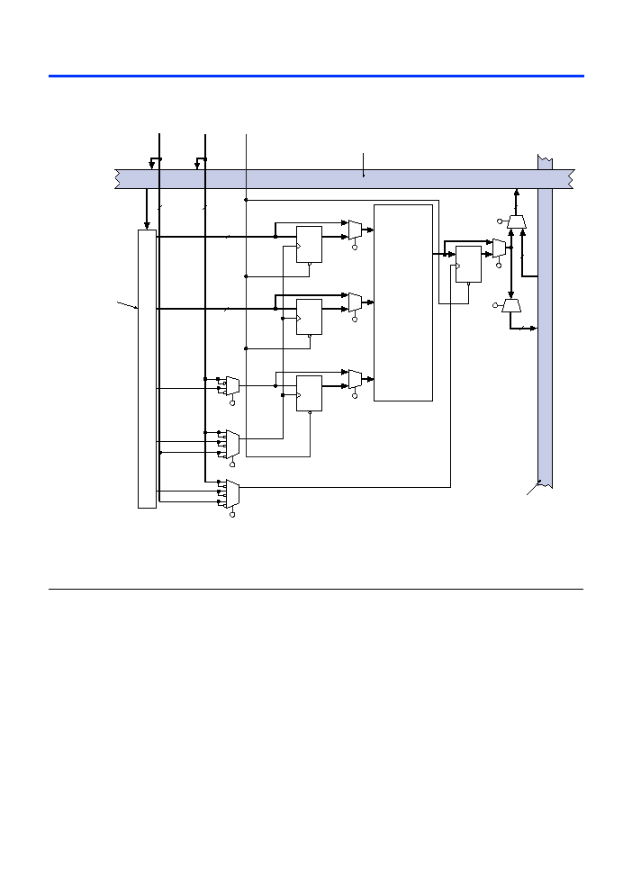
The EAB can also be used for bidirectional, dual-port memory
applications where two ports read or write simultaneously. To implement
this type of dual-port memory, two EABs are used to support two
simultaneous read or writes.
Alternatively, one clock and clock enable can be used to control the input
registers of the EAB, while a different clock and clock enable control the
output registers (see
Figure 2
).
Figure 2. FLEX 10KE Device in Dual-Port RAM Mode
Notes (1)
Notes:
(1)
All registers can be asynchronously cleared by EAB local interconnect signals, global signals, or the chip-wide reset.
(2)
EPF10K30E and EPF10K50E devices have 88 EAB local interconnect channels; EPF10K100E, EPF10K130E, and
EPF10K200E devices have 104 EAB local interconnect channels.
Column Interconnect
EAB Local
Interconnect (2)
Dedicated Clocks
2
4
D
ENA
Q
D
ENA
Q
D
ENA
Q
D
ENA
Q
D
ENA
Q
data[ ]
rdaddress[ ]
wraddress[ ]
RAM/ROM
256
◊
16
512
◊
8
1,024
◊
4
2,048
◊
2
Data In
Read Address
Write Address
Read Enable
Write Enable
Data Out
4, 8, 16, 32
4, 8, 16, 32
outclocken
inclocken
inclock
outclock
D
ENA
Q
Write
Pulse
Generator
rden
wren
Multiplexers allow read
address and read
enable registers to be
clocked by inclock or
outclock signals.
Row Interconnect
4, 8
Dedicated Inputs &
Global Signals

12
Altera Corporation
FLEX 10KE Embedded Programmable Logic Devices Data Sheet
The EAB can also use Altera megafunctions to implement dual-port RAM
applications where both ports can read or write, as shown in
Figure 3
.
Figure 3. FLEX 10KE EAB in Dual-Port RAM Mode
The FLEX 10KE EAB can be used in a single-port mode, which is useful for
backward-compatibility with FLEX 10K designs (see
Figure 4
).
Port A
Port B
address_a[]
address_b[]
data_a[]
data_b[]
we_a
we_b
clkena_a
clkena_b
Clock A
Clock B
Altera Corporation
13
FLEX 10KE Embedded Programmable Logic Devices Data Sheet
Figure 4. FLEX 10KE Device in Single-Port RAM Mode
Note:
(1)
EPF10K30E, EPF10K50E, and EPF10K50S devices have 88 EAB local interconnect channels; EPF10K100E,
EPF10K130E, EPF10K200E, and EPF10K200S devices have 104 EAB local interconnect channels.
EABs can be used to implement synchronous RAM, which is easier to use
than asynchronous RAM. A circuit using asynchronous RAM must
generate the RAM write enable signal, while ensuring that its data and
address signals meet setup and hold time specifications relative to the
write enable signal. In contrast, the EAB's synchronous RAM generates its
own write enable signal and is self-timed with respect to the input or write
clock. A circuit using the EAB's self-timed RAM must only meet the setup
and hold time specifications of the global clock.
Column Interconnect
EAB Local
Interconnect (1)
Dedicated Inputs
& Global Signals
D
Q
D
Q
RAM/ROM
256
◊
16
512
◊
8
1,024
◊
4
2,048
◊
2
Data In
Address
Write Enable
Data Out
4, 8, 16, 32
4, 8, 16, 32
D
Q
D
Q
4
8, 4, 2, 1
8, 9, 10, 11
Row Interconnect
Dedicated
Clocks
2
4, 8
Chip-Wide
Reset
14
Altera Corporation
FLEX 10KE Embedded Programmable Logic Devices Data Sheet
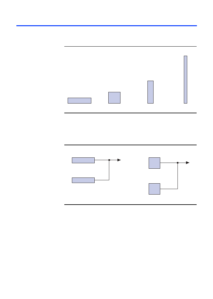
When used as RAM, each EAB can be configured in any of the following
sizes: 256
◊
16, 512
◊
8, 1,024
◊
4, or 2,048
◊
2 (see
Figure 5
).
Figure 5. FLEX 10KE EAB Memory Configurations
Larger blocks of RAM are created by combining multiple EABs. For
example, two 256
◊
16 RAM blocks can be combined to form a 256
◊
32
block; two 512
◊
8 RAM blocks can be combined to form a 512
◊
16 block
(see
Figure 6
).
Figure 6. Examples of Combining FLEX 10KE EABs
If necessary, all EABs in a device can be cascaded to form a single RAM
block. EABs can be cascaded to form RAM blocks of up to 2,048 words
without impacting timing. The Altera software automatically combines
EABs to meet a designer's RAM specifications.
256
◊
16
512
◊
8
1,024
◊
4
2,048
◊
2
512
◊
8
512
◊
8
256
◊
16
256
◊
16
256
◊
32
512
◊
16

Altera Corporation
15
FLEX 10KE Embedded Programmable Logic Devices Data Sheet
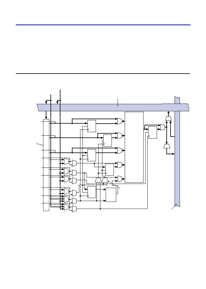
EABs provide flexible options for driving and controlling clock signals.
Different clocks and clock enables can be used for reading and writing to
the EAB. Registers can be independently inserted on the data input, EAB
output, write address, write enable signals, read address, and read enable
signals. The global signals and the EAB local interconnect can drive write
enable, read enable, and clock enable signals. The global signals,
dedicated clock pins, and EAB local interconnect can drive the EAB clock
signals. Because the LEs drive the EAB local interconnect, the LEs can
control write enable, read enable, clear, clock, and clock enable signals.
An EAB is fed by a row interconnect and can drive out to row and column
interconnects. Each EAB output can drive up to two row channels and up
to two column channels; the unused row channel can be driven by other
LEs. This feature increases the routing resources available for EAB
outputs (see
Figures 2
and
4
). The column interconnect, which is adjacent
to the EAB, has twice as many channels as other columns in the device.
Logic Array Block
An LAB consists of eight LEs, their associated carry and cascade chains,
LAB control signals, and the LAB local interconnect. The LAB provides
the coarse-grained structure to the FLEX 10KE architecture, facilitating
efficient routing with optimum device utilization and high performance
(see
Figure 7
).
16
Altera Corporation
FLEX 10KE Embedded Programmable Logic Devices Data Sheet
Figure 7. FLEX 10KE LAB
Notes:
(1)
EPF10K30E, EPF10K50E, and EPF10K50S devices have 22 inputs to the LAB local interconnect channel from the
row; EPF10K100E, EPF10K130E, EPF10K200E, and EPF10K200S devices have 26.
(2)
EPF10K30E, EPF10K50E, and EPF10K50S devices have 30 LAB local interconnect channels; EPF10K100E,
EPF10K130E, EPF10K200E, and EPF10K200S devices have 34.
2
8
Carry-In &
Cascade-In
LE1
LE8
LE2
LE3
LE4
LE5
LE6
LE7
Column
Interconnect
ter
ter
Row Interconnect
ter
ter
(1)
LAB Local
Interconnect (2
ter
ter
)
(2
(2
Column-to-Row
Interconnect
ter
ter
Carry-Out &
Cascade-Out
16
24 to 48
to
to
LAB Control
Signals
nal
nal
See Figure 12
for details.
6
Dedicated Inputs &
Global Signals
16
6
8
4
4
4
4
4
4
4
4
4
4
2
8

Altera Corporation
17
FLEX 10KE Embedded Programmable Logic Devices Data Sheet
Each LAB provides four control signals with programmable inversion
that can be used in all eight LEs. Two of these signals can be used as clocks,
the other two can be used for clear/preset control. The LAB clocks can be
driven by the dedicated clock input pins, global signals, I/O signals, or
internal signals via the LAB local interconnect. The LAB preset and clear
control signals can be driven by the global signals, I/O signals, or internal
signals via the LAB local interconnect. The global control signals are
typically used for global clock, clear, or preset signals because they
provide asynchronous control with very low skew across the device. If
logic is required on a control signal, it can be generated in one or more LE
in any LAB and driven into the local interconnect of the target LAB. In
addition, the global control signals can be generated from LE outputs.
Logic Element
The LE, the smallest unit of logic in the FLEX 10KE architecture, has a
compact size that provides efficient logic utilization. Each LE contains a
four-input LUT, which is a function generator that can quickly compute
any function of four variables. In addition, each LE contains a
programmable flipflop with a synchronous clock enable, a carry chain,
and a cascade chain. Each LE drives both the local and the FastTrack
Interconnect routing structure (see
Figure 8
).
Figure 8. FLEX 10KE Logic Element
LAB Local
Interconnect
Carry-In
Clock
Select
Carry-Out
Look-Up
Table
(LUT)
Clear/
Preset
Logic
Carry
Chain
Cascade
Chain
Cascade-In
Cascade-Out
FastTrack
Interconnect
Programmable
Register
PRN
CLRN
D
Q
ENA
Register Bypass
data1
data2
data3
data4
labctrl1
labctrl2
labctrl4
labctrl3
Chip-Wide
Reset

18
Altera Corporation
FLEX 10KE Embedded Programmable Logic Devices Data Sheet
The programmable flipflop in the LE can be configured for D, T, JK, or SR
operation. The clock, clear, and preset control signals on the flipflop can
be driven by global signals, general-purpose I/O pins, or any internal
logic. For combinatorial functions, the flipflop is bypassed and the output
of the LUT drives the output of the LE.
The LE has two outputs that drive the interconnect: one drives the local
interconnect and the other drives either the row or column FastTrack
Interconnect routing structure. The two outputs can be controlled
independently. For example, the LUT can drive one output while the
register drives the other output. This feature, called register packing, can
improve LE utilization because the register and the LUT can be used for
unrelated functions.
The FLEX 10KE architecture provides two types of dedicated high-speed
data paths that connect adjacent LEs without using local interconnect
paths: carry chains and cascade chains. The carry chain supports
high-speed counters and adders and the cascade chain implements
wide-input functions with minimum delay. Carry and cascade chains
connect all LEs in a LAB as well as all LABs in the same row. Intensive use
of carry and cascade chains can reduce routing flexibility. Therefore, the
use of these chains should be limited to speed-critical portions of a design.
Carry Chain
The carry chain provides a very fast (as low as 0.2 ns) carry-forward
function between LEs. The carry-in signal from a lower-order bit drives
forward into the higher-order bit via the carry chain, and feeds into both
the LUT and the next portion of the carry chain. This feature allows the
FLEX 10KE architecture to implement high-speed counters, adders, and
comparators of arbitrary width efficiently. Carry chain logic can be
created automatically by the Altera Compiler during design processing,
or manually by the designer during design entry. Parameterized functions
such as LPM and DesignWare functions automatically take advantage of
carry chains.
Carry chains longer than eight LEs are automatically implemented by
linking LABs together. For enhanced fitting, a long carry chain skips
alternate LABs in a row. A carry chain longer than one LAB skips either
from even-numbered LAB to even-numbered LAB, or from odd-
numbered LAB to odd-numbered LAB. For example, the last LE of the
first LAB in a row carries to the first LE of the third LAB in the row. The
carry chain does not cross the EAB at the middle of the row. For instance,
in the EPF10K50E device, the carry chain stops at the eighteenth LAB and
a new one begins at the nineteenth LAB.

Altera Corporation
19
FLEX 10KE Embedded Programmable Logic Devices Data Sheet
Figure 9
shows how an n-bit full adder can be implemented in n + 1 LEs
with the carry chain. One portion of the LUT generates the sum of two bits
using the input signals and the carry-in signal; the sum is routed to the
output of the LE. The register can be bypassed for simple adders or used
for an accumulator function. Another portion of the LUT and the carry
chain logic generates the carry-out signal, which is routed directly to the
carry-in signal of the next-higher-order bit. The final carry-out signal is
routed to an LE, where it can be used as a general-purpose signal.
Figure 9. FLEX 10KE Carry Chain Operation (n-Bit Full Adder)
LUT
a1
b1
Carry Chain
s1
LE1
Register
a2
b2
Carry Chain
s2
LE2
Register
Carry Chain
sn
LEn
Register
an
bn
Carry Chain
Carry-Out
LEn + 1
Register
Carry-In
LUT
LUT
LUT

20
Altera Corporation
FLEX 10KE Embedded Programmable Logic Devices Data Sheet
Cascade Chain
With the cascade chain, the FLEX 10KE architecture can implement
functions that have a very wide fan-in. Adjacent LUTs can be used to
compute portions of the function in parallel; the cascade chain serially
connects the intermediate values. The cascade chain can use a logical
AND
or logical
OR
(via De Morgan's inversion) to connect the outputs of
adjacent LEs. An a delay as low as 0.6 ns per LE, each additional LE
provides four more inputs to the effective width of a function. Cascade
chain logic can be created automatically by the Altera Compiler during
design processing, or manually by the designer during design entry.
Cascade chains longer than eight bits are implemented automatically by
linking several LABs together. For easier routing, a long cascade chain
skips every other LAB in a row. A cascade chain longer than one LAB
skips either from even-numbered LAB to even-numbered LAB, or from
odd-numbered LAB to odd-numbered LAB (e.g., the last LE of the first
LAB in a row cascades to the first LE of the third LAB). The cascade chain
does not cross the center of the row (e.g., in the EPF10K50E device, the
cascade chain stops at the eighteenth LAB and a new one begins at the
nineteenth LAB). This break is due to the EAB's placement in the middle
of the row.
Figure 10
shows how the cascade function can connect adjacent LEs to
form functions with a wide fan-in. These examples show functions of
4n variables implemented with n LEs. The LE delay is 0.9 ns; the cascade
chain delay is 0.6 ns. With the cascade chain, 2.7 ns are needed to decode
a 16-bit address.
Figure 10. FLEX 10KE Cascade Chain Operation
LE1
LUT
LE2
LUT
d[3..0]
d[7..4]
d[(4n ≠ 1)..(4n ≠ 4)]
d[3..0]
d[7..4]
LEn
LE1
LE2
LEn
LUT
LUT
LUT
LUT
AND Cascade Chain
OR Cascade Chain
d[(4n ≠ 1)..(4n ≠ 4)]

Altera Corporation
21
FLEX 10KE Embedded Programmable Logic Devices Data Sheet
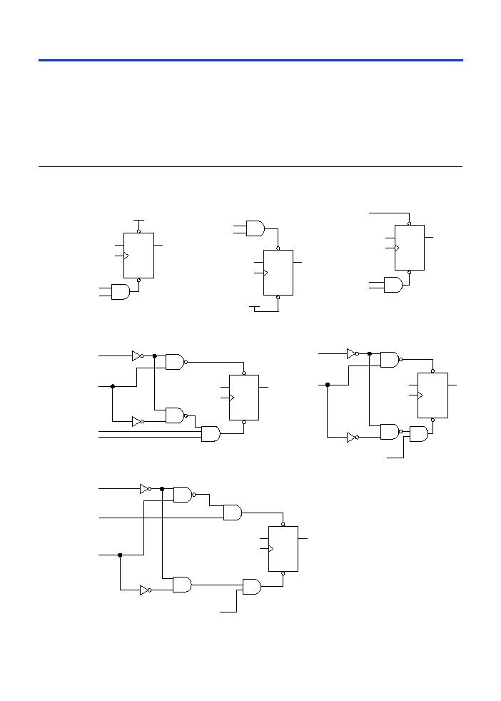
LE Operating Modes
The FLEX 10KE LE can operate in the following four modes:
Normal mode
Arithmetic mode
Up/down counter mode
Clearable counter mode
Each of these modes uses LE resources differently. In each mode, seven
available inputs to the LE--the four data inputs from the LAB local
interconnect, the feedback from the programmable register, and the
carry-in and cascade-in from the previous LE--are directed to different
destinations to implement the desired logic function. Three inputs to the
LE provide clock, clear, and preset control for the register. The Altera
software, in conjunction with parameterized functions such as LPM and
DesignWare functions, automatically chooses the appropriate mode for
common functions such as counters, adders, and multipliers. If required,
the designer can also create special-purpose functions that use a specific
LE operating mode for optimal performance.
The architecture provides a synchronous clock enable to the register in all
four modes. The Altera software can set
DATA1
to enable the register
synchronously, providing easy implementation of fully synchronous
designs.

22
Altera Corporation
FLEX 10KE Embedded Programmable Logic Devices Data Sheet
Figure 11
shows the LE operating modes.
Figure 11. FLEX 10KE LE Operating Modes
ENA
PRN
CLRN
D
Q
4-Input
LUT
Carry-In
Cascade-Out
Cascade-In
LE-Out to FastTrack
Interconnect
LE-Out to Local
Interconnect
ENA
Normal Mode
PRN
CLRN
D
Q
Cascade-Out
LE-Out
Cascade-In
3-Input
LUT
Carry-In
3-Input
LUT
Carry-Out
Arithmetic Mode
Up/Down Counter Mode
PRN
CLRN
D
Q
3-Input
LUT
Carry-In
Cascade-In
LE-Out
3-Input
LUT
Carry-Out
1
0
Cascade-Out
Clearable Counter Mode
PRN
CLRN
D
Q
3-Input
LUT
Carry-In
LE-Out
3-Input
LUT
Carry-Out
1
0
Cascade-Out
ENA
ENA
data1
data4
data3
data2
data1
data2
data1 (ena)
data2 (u/d)
data4 (nload)
data3 (data)
data1 (ena)
data2 (nclr)
data4 (nload)
data3 (data)

Altera Corporation
23
FLEX 10KE Embedded Programmable Logic Devices Data Sheet
Normal Mode
The normal mode is suitable for general logic applications and wide
decoding functions that can take advantage of a cascade chain. In normal
mode, four data inputs from the LAB local interconnect and the carry-in
are inputs to a four-input LUT. The Altera Compiler automatically selects
the carry-in or the
DATA3
signal as one of the inputs to the LUT. The LUT
output can be combined with the cascade-in signal to form a cascade chain
through the cascade-out signal. Either the register or the LUT can be used
to drive both the local interconnect and the FastTrack Interconnect routing
structure at the same time.
The LUT and the register in the LE can be used independently (register
packing). To support register packing, the LE has two outputs; one drives
the local interconnect, and the other drives the FastTrack Interconnect
routing structure. The
DATA4
signal can drive the register directly,
allowing the LUT to compute a function that is independent of the
registered signal; a three-input function can be computed in the LUT, and
a fourth independent signal can be registered. Alternatively, a four-input
function can be generated, and one of the inputs to this function can be
used to drive the register. The register in a packed LE can still use the clock
enable, clear, and preset signals in the LE. In a packed LE, the register can
drive the FastTrack Interconnect routing structure while the LUT drives
the local interconnect, or vice versa.
Arithmetic Mode
The arithmetic mode offers 2 three-input LUTs that are ideal for
implementing adders, accumulators, and comparators. One LUT
computes a three-input function; the other generates a carry output. As
shown in
Figure 11
on
page 22
, the first LUT uses the carry-in signal and
two data inputs from the LAB local interconnect to generate a
combinatorial or registered output. For example, in an adder, this output
is the sum of three signals:
a
,
b
, and carry-in. The second LUT uses the
same three signals to generate a carry-out signal, thereby creating a carry
chain. The arithmetic mode also supports simultaneous use of the cascade
chain.
Up/Down Counter Mode
The up/down counter mode offers counter enable, clock enable,
synchronous up/down control, and data loading options. These control
signals are generated by the data inputs from the LAB local interconnect,
the carry-in signal, and output feedback from the programmable register.
Use 2 three-input LUTs: one generates the counter data, and the other
generates the fast carry bit. A 2-to-1 multiplexer provides synchronous
loading. Data can also be loaded asynchronously with the clear and preset
register control signals without using the LUT resources.

24
Altera Corporation
FLEX 10KE Embedded Programmable Logic Devices Data Sheet
Clearable Counter Mode
The clearable counter mode is similar to the up/down counter mode, but
supports a synchronous clear instead of the up/down control. The clear
function is substituted for the cascade-in signal in the up/down counter
mode. Use 2 three-input LUTs: one generates the counter data, and the
other generates the fast carry bit. Synchronous loading is provided by a
2-to-1 multiplexer. The output of this multiplexer is
AND
ed with a
synchronous clear signal.
Internal Tri-State Emulation
Internal tri-state emulation provides internal tri-states without the
limitations of a physical tri-state bus. In a physical tri-state bus, the
tri-state buffers' output enable (
OE
) signals select which signal drives the
bus. However, if multiple
OE
signals are active, contending signals can be
driven onto the bus. Conversely, if no
OE
signals are active, the bus will
float. Internal tri-state emulation resolves contending tri-state buffers to a
low value and floating buses to a high value, thereby eliminating these
problems. The Altera software automatically implements tri-state bus
functionality with a multiplexer.
Clear & Preset Logic Control
Logic for the programmable register's clear and preset functions is
controlled by the
DATA3
,
LABCTRL1
, and
LABCTRL2
inputs to the LE. The
clear and preset control structure of the LE asynchronously loads signals
into a register. Either
LABCTRL1
or
LABCTRL2
can control the
asynchronous clear. Alternatively, the register can be set up so that
LABCTRL1
implements an asynchronous load. The data to be loaded is
driven to
DATA3
; when
LABCTRL1
is asserted,
DATA3
is loaded into the
register.
During compilation, the Altera Compiler automatically selects the best
control signal implementation. Because the clear and preset functions are
active-low, the Compiler automatically assigns a logic high to an unused
clear or preset.
The clear and preset logic is implemented in one of the following six
modes chosen during design entry:
Asynchronous clear
Asynchronous preset
Asynchronous clear and preset
Asynchronous load with clear
Asynchronous load with preset
Asynchronous load without clear or preset
Altera Corporation
25
FLEX 10KE Embedded Programmable Logic Devices Data Sheet
In addition to the six clear and preset modes, FLEX 10KE devices provide
a chip-wide reset pin that can reset all registers in the device. Use of this
feature is set during design entry. In any of the clear and preset modes, the
chip-wide reset overrides all other signals. Registers with asynchronous
presets may be preset when the chip-wide reset is asserted. Inversion can
be used to implement the asynchronous preset.
Figure 12
shows examples
of how to setup the preset and clear inputs for the desired functionality.
Figure 12. FLEX 10KE LE Clear & Preset Modes
Asynchronous Clear
Asynchronous Preset
Asynchronous Preset & Clear
Asynchronous Load without Clear or Preset
labctrl1
(Asynchronous
Load)
PRN
CLRN
D
Q
NOT
NOT
labctrl1
(Asynchronous
Load)
Asynchronous Load with Clear
labctrl2
(Clear)
PRN
CLRN
D
Q
NOT
NOT
(Asynchronous
Load)
Asynchronous Load with Preset
NOT
NOT
PRN
CLRN
D
Q
labctrl1 or
labctrl2
PRN
CLRN
D
Q
VCC
Chip-Wide Reset
Chip-Wide Reset
Chip-Wide Reset
Chip-Wide Reset
PRN
CLRN
D
Q
PRN
CLRN
D
Q
VCC
Chip-Wide
Reset
Chip-Wide Reset
data3
(Data)
labctrl1
labctrl2
(Preset)
data3
(Data)
data3
(Data)
labctrl1 or
labctrl2
labctrl1
labctrl2

26
Altera Corporation
FLEX 10KE Embedded Programmable Logic Devices Data Sheet
Asynchronous Clear
The flipflop can be cleared by either
LABCTRL1
or
LABCTRL2
. In this
mode, the preset signal is tied to
VCC
to deactivate it.
Asynchronous Preset
An asynchronous preset is implemented as an asynchronous load, or with
an asynchronous clear. If
DATA3
is tied to
VCC
, asserting
LABCTRL1
asynchronously loads a one into the register. Alternatively, the Altera
software can provide preset control by using the clear and inverting the
input and output of the register. Inversion control is available for the
inputs to both LEs and IOEs. Therefore, if a register is preset by only one
of the two
LABCTRL
signals, the
DATA3
input is not needed and can be
used for one of the LE operating modes.
Asynchronous Preset & Clear
When implementing asynchronous clear and preset,
LABCTRL1
controls
the preset and
LABCTRL2
controls the clear.
DATA3
is tied to
VCC
, so that
asserting
LABCTRL1
asynchronously loads a one into the register,
effectively presetting the register. Asserting
LABCTRL2
clears the register.
Asynchronous Load with Clear
When implementing an asynchronous load in conjunction with the clear,
LABCTRL1
implements the asynchronous load of
DATA3
by controlling
the register preset and clear.
LABCTRL2
implements the clear by
controlling the register clear;
LABCTRL2
does not have to feed the preset
circuits.
Asynchronous Load with Preset
When implementing an asynchronous load in conjunction with preset, the
Altera software provides preset control by using the clear and inverting
the input and output of the register. Asserting
LABCTRL2
presets the
register, while asserting
LABCTRL1
loads the register. The Altera software
inverts the signal that drives
DATA3
to account for the inversion of the
register's output.
Asynchronous Load without Preset or Clear
When implementing an asynchronous load without preset or clear,
LABCTRL1
implements the asynchronous load of
DATA3
by controlling
the register preset and clear.

Altera Corporation
27
FLEX 10KE Embedded Programmable Logic Devices Data Sheet
FastTrack Interconnect Routing Structure
In the FLEX 10KE architecture, connections between LEs, EABs, and
device I/O pins are provided by the FastTrack Interconnect routing
structure, which is a series of continuous horizontal and vertical routing
channels that traverses the device. This global routing structure provides
predictable performance, even in complex designs. In contrast, the
segmented routing in FPGAs requires switch matrices to connect a
variable number of routing paths, increasing the delays between logic
resources and reducing performance.
The FastTrack Interconnect routing structure consists of row and column
interconnect channels that span the entire device. Each row of LABs is
served by a dedicated row interconnect. The row interconnect can drive
I/O pins and feed other LABs in the row. The column interconnect routes
signals between rows and can drive I/O pins.
Row channels drive into the LAB or EAB local interconnect. The row
signal is buffered at every LAB or EAB to reduce the effect of fan-out on
delay. A row channel can be driven by an LE or by one of three column
channels. These four signals feed dual 4-to-1 multiplexers that connect to
two specific row channels. These multiplexers, which are connected to
each LE, allow column channels to drive row channels even when all eight
LEs in a LAB drive the row interconnect.
Each column of LABs or EABs is served by a dedicated column
interconnect. The column interconnect that serves the EABs has twice as
many channels as other column interconnects. The column interconnect
can then drive I/O pins or another row's interconnect to route the signals
to other LABs or EABs in the device. A signal from the column
interconnect, which can be either the output of a LE or an input from an
I/O pin, must be routed to the row interconnect before it can enter a LAB
or EAB. Each row channel that is driven by an IOE or EAB can drive one
specific column channel.
Access to row and column channels can be switched between LEs in
adjacent pairs of LABs. For example, a LE in one LAB can drive the row
and column channels normally driven by a particular LE in the adjacent
LAB in the same row, and vice versa. This flexibility enables routing
resources to be used more efficiently (see
Figure 13
).

28
Altera Corporation
FLEX 10KE Embedded Programmable Logic Devices Data Sheet
Figure 13. FLEX 10KE LAB Connections to Row & Column Interconnect
From Adjacent LAB
Row Channels
Column
Channels
Each LE can drive two
row channels.
LE 2
LE 8
LE 1
To Adjacent LAB
Each LE can switch
interconnect access
with an LE in the
adjacent LAB.
At each intersection,
six row channels can
drive column channels.
To Other Rows
To LAB Local
Interconnect
To Other
Columns

Altera Corporation
29
FLEX 10KE Embedded Programmable Logic Devices Data Sheet
For improved routing, the row interconnect consists of a combination of
full-length and half-length channels. The full-length channels connect to
all LABs in a row; the half-length channels connect to the LABs in half of
the row. The EAB can be driven by the half-length channels in the left half
of the row and by the full-length channels. The EAB drives out to the full-
length channels. In addition to providing a predictable, row-wide
interconnect, this architecture provides increased routing resources. Two
neighboring LABs can be connected using a half-row channel, thereby
saving the other half of the channel for the other half of the row.
Table 7
summarizes the FastTrack Interconnect routing structure
resources available in each FLEX 10KE device.
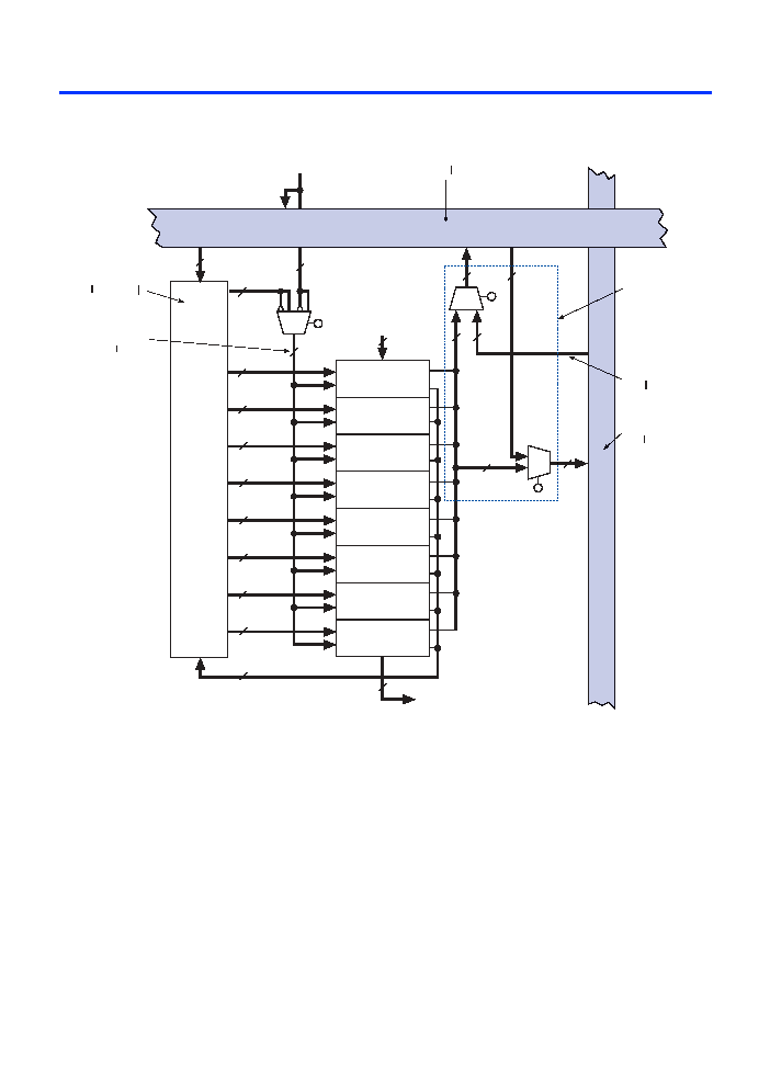
In addition to general-purpose I/O pins, FLEX 10KE devices have six
dedicated input pins that provide low-skew signal distribution across the
device. These six inputs can be used for global clock, clear, preset, and
peripheral output enable and clock enable control signals. These signals
are available as control signals for all LABs and IOEs in the device. The
dedicated inputs can also be used as general-purpose data inputs because
they can feed the local interconnect of each LAB in the device.
Figure 14
shows the interconnection of adjacent LABs and EABs, with
row, column, and local interconnects, as well as the associated cascade
and carry chains. Each LAB is labeled according to its location: a letter
represents the row and a number represents the column. For example,
LAB B3 is in row B, column 3.
Table 7. FLEX 10KE FastTrack Interconnect Resources
Device
Rows
Channels per
Row
Columns
Channels per
Column
EPF10K30E
6
216
36
24
EPF10K50E
EPF10K50S
10
216
36
24
EPF10K100E
12
312
52
24
EPF10K130E
16
312
52
32
EPF10K200E
EPF10K200S
24
312
52
48
30
Altera Corporation
FLEX 10KE Embedded Programmable Logic Devices Data Sheet
Figure 14. FLEX 10KE Interconnect Resources
I/O Element
An IOE contains a bidirectional I/O buffer and a register that can be used
either as an input register for external data that requires a fast setup time,
or as an output register for data that requires fast clock-to-output
performance. In some cases, using an LE register for an input register will
result in a faster setup time than using an IOE register. IOEs can be used
as input, output, or bidirectional pins. For bidirectional registered I/O
implementation, the output register should be in the IOE, and the data
input and output enable registers should be LE registers placed adjacent
to the bidirectional pin. The Altera Compiler uses the programmable
inversion option to invert signals from the row and column interconnect
automatically where appropriate.
Figure 15
shows the bidirectional I/O
registers.
I/O Element (IOE)
Row
Interconnect
IOE
IOE
IOE
IOE
Column
Interconnect
LAB
B1
See Figure 17
for details.
See Figure 16
for details.
LAB
A3
LAB
B3
LAB
A1
LAB
A2
LAB
B2
IOE
IOE
Cascade &
LAB B4
LAB A4
LAB B5
LAB A5
IOE
IOE
IOE
IOE
IOE
IOE
IOE
IOE
IOE
IOE
IOE
IOE
IOE
IOE
Carry Chains

Altera Corporation
31
FLEX 10KE Embedded Programmable Logic Devices Data Sheet
Figure 15. FLEX 10KE Bidirectional I/O Registers
Note:
(1)
All FLEX 10KE devices (except the EPF10K50E and EPF10K200E devices) have a programmable input delay buffer
on the input path.
VCC
OE[7..0]
CLK[1..0]
ENA[5..0]
CLRN[1..0]
Peripheral
Control Bus
CLRN
D
Q
ENA
VCC
2 Dedicated
Clock Inputs
Slew-Rate
Control
Open-Drain
Output
Chip-Wide
Output Enable
CLK[3..2]
2
12
VCC
VCC
Chip-Wide
Reset
Programmable Delay
(1)
4 Dedicated
Inputs
Row and Column
Interconnect
4
VCC
CLRN
D
Q
ENA
Chip-Wide
Reset
CLRN
D
Q
ENA
Chip-Wide
Reset
VCC
Input Register
(2)
Output Register
(2)
OE Register

32
Altera Corporation
FLEX 10KE Embedded Programmable Logic Devices Data Sheet
On all FLEX 10KE devices (except EPF10K50E and EPF10K200E devices),
the input path from the I/O pad to the FastTrack Interconnect has a
programmable delay element that can be used to guarantee a zero hold
time. EPF10K50S and EPF10K200S devices also support this feature.
Depending on the placement of the IOE relative to what it is driving, the
designer may choose to turn on the programmable delay to ensure a zero
hold time or turn it off to minimize setup time. This feature is used to
reduce setup time for complex pin-to-register paths (e.g., PCI designs).
Each IOE selects the clock, clear, clock enable, and output enable controls
from a network of I/O control signals called the peripheral control bus.
The peripheral control bus uses high-speed drivers to minimize signal
skew across the device and provides up to 12 peripheral control signals
that can be allocated as follows:
Up to eight output enable signals
Up to six clock enable signals
Up to two clock signals
Up to two clear signals
If more than six clock enable or eight output enable signals are required,
each IOE on the device can be controlled by clock enable and output
enable signals driven by specific LEs. In addition to the two clock signals
available on the peripheral control bus, each IOE can use one of two
dedicated clock pins. Each peripheral control signal can be driven by any
of the dedicated input pins or the first LE of each LAB in a particular row.
In addition, a LE in a different row can drive a column interconnect, which
causes a row interconnect to drive the peripheral control signal. The chip-
wide reset signal resets all IOE registers, overriding any other control
signals.
When a dedicated clock pin drives IOE registers, it can be inverted for all
IOEs in the device. All IOEs must use the same sense of the clock. For
example, if any IOE uses the inverted clock, all IOEs must use the inverted
clock and no IOE can use the non-inverted clock. However, LEs can still
use the true or complement of the clock on a LAB-by-LAB basis.
The incoming signal may be inverted at the dedicated clock pin and will
drive all IOEs. For the true and complement of a clock to be used to drive
IOEs, drive it into both global clock pins. One global clock pin will supply
the true, and the other will supply the complement.
When the true and complement of a dedicated input drives IOE clocks,
two signals on the peripheral control bus are consumed, one for each
sense of the clock.

Altera Corporation
33
FLEX 10KE Embedded Programmable Logic Devices Data Sheet
When dedicated inputs drive non-inverted and inverted peripheral clears,
clock enables, and output enables, two signals on the peripheral control
bus will be used.
Tables 8
and
9
list the sources for each peripheral control signal, and show
how the output enable, clock enable, clock, and clear signals share
12 peripheral control signals. The tables also show the rows that can drive
global signals.
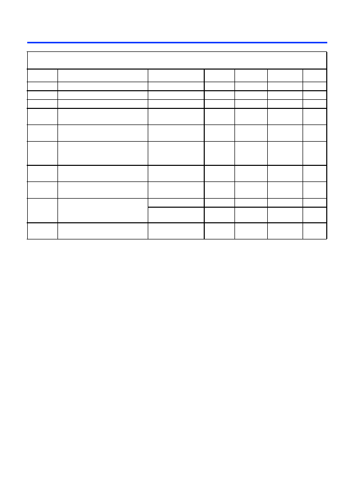
Table 8. Peripheral Bus Sources for EPF10K30E, EPF10K50E & EPF10K50S Devices
Peripheral
Control Signal
EPF10K30E
EPF10K50E
EPF10K50S
OE0
Row A
Row A
OE1
Row B
Row B
OE2
Row C
Row D
OE3
Row D
Row F
OE4
Row E
Row H
OE5
Row F
Row J
CLKENA0/CLK0/GLOBAL0
Row A
Row A
CLKENA1/OE6/GLOBAL1
Row B
Row C
CLKENA2/CLR0
Row C
Row E
CLKENA3/OE7/GLOBAL2
Row D
Row G
CLKENA4/CLR1
Row E
Row I
CLKENA5/CLK1/GLOBAL3
Row F
Row J

34
Altera Corporation
FLEX 10KE Embedded Programmable Logic Devices Data Sheet
Signals on the peripheral control bus can also drive the four global signals,
referred to as
GLOBAL0
through
GLOBAL3
in
Tables 8
and
9
. An internally
generated signal can drive a global signal, providing the same low-skew,
low-delay characteristics as a signal driven by an input pin. An LE drives
the global signal by driving a row line that drives the peripheral bus,
which then drives the global signal. This feature is ideal for internally
generated clear or clock signals with high fan-out. However, internally
driven global signals offer no advantage over the general-purpose
interconnect for routing data signals. The dedicated input pin should be
driven to a known logic state (such as ground) and not be allowed to float.
The chip-wide output enable pin is an active-high pin (
DEV_OE
) that can
be used to tri-state all pins on the device. This option can be set in the
Altera software. On EPF10K50E and EPF10K200E devices, the built-in I/O
pin pull-up resistors (which are active during configuration) are active
when the chip-wide output enable pin is asserted. The registers in the IOE
can also be reset by the chip-wide reset pin.
Table 9. Peripheral Bus Sources for EPF10K100E, EPF10K130E, EPF10K200E & EPF10K200S Devices
Peripheral
Control Signal
EPF10K100E
EPF10K130E
EPF10K200E
EPF10K200S
OE0
Row A
Row C
Row G
OE1
Row C
Row E
Row I
OE2
Row E
Row G
Row K
OE3
Row L
Row N
Row R
OE4
Row I
Row K
Row O
OE5
Row K
Row M
Row Q
CLKENA0/CLK0/GLOBAL0
Row F
Row H
Row L
CLKENA1/OE6/GLOBAL1
Row D
Row F
Row J
CLKENA2/CLR0
Row B
Row D
Row H
CLKENA3/OE7/GLOBAL2
Row H
Row J
Row N
CLKENA4/CLR1
Row J
Row L
Row P
CLKENA5/CLK1/GLOBAL3
Row G
Row I
Row M

Altera Corporation
35
FLEX 10KE Embedded Programmable Logic Devices Data Sheet
Row-to-IOE Connections
When an IOE is used as an input signal, it can drive two separate row
channels. The signal is accessible by all LEs within that row. When an IOE
is used as an output, the signal is driven by a multiplexer that selects a
signal from the row channels. Up to eight IOEs connect to each side of
each row channel (see
Figure 16
).
Figure 16. FLEX 10KE Row-to-IOE Connections
Table 10
lists the FLEX 10KE row-to-IOE interconnect resources.
n
n
Each IOE is driven by an
m-to-1 multiplexer.
Each IOE can drive two
row channels.
IOE8
IOE1
m
m
Row FastTrack
Interconnect
n
The values for m and n are provided in
Table 10
.
Table 10. FLEX 10KE Row-to-IOE Interconnect Resources
Device
Channels per Row (n)
Row Channels per Pin (m)
EPF10K30E
216
27
EPF10K50E
EPF10K50S
216
27
EPF10K100E
312
39
EPF10K130E
312
39
EPF10K200E
EPF10K200S
312
39

36
Altera Corporation
FLEX 10KE Embedded Programmable Logic Devices Data Sheet
Column-to-IOE Connections
When an IOE is used as an input, it can drive up to two separate column
channels. When an IOE is used as an output, the signal is driven by a
multiplexer that selects a signal from the column channels. Two IOEs
connect to each side of the column channels. Each IOE can be driven by
column channels via a multiplexer. The set of column channels is different
for each IOE (see
Figure 17
).
Figure 17. FLEX 10KE Column-to-IOE Connections
Table 11
lists the FLEX 10KE column-to-IOE interconnect resources.
Each IOE is driven by
a
m
-to-1 multiplexer
Each IOE can drive two
column channels.
Column
Interconnect
n
n
m
m
n
IOE1
IOE1
The values for m and n are provided in
Table 11
.
Table 11. FLEX 10KE Column-to-IOE Interconnect Resources
Device
Channels per Column (n)
Column Channels per Pin (m)
EPF10K30E
24
16
EPF10K50E
EPF10K50S
24
16
EPF10K100E
24
16
EPF10K130E
32
24
EPF10K200E
EPF10K200S
48
40

Altera Corporation
37
FLEX 10KE Embedded Programmable Logic Devices Data Sheet
SameFrame
Pin-Outs
FLEX 10KE devices support the SameFrame pin-out feature for
FineLine BGA packages. The SameFrame pin-out feature is the
arrangement of balls on FineLine BGA packages such that the lower-ball-
count packages form a subset of the higher-ball-count packages.
SameFrame pin-outs provide the flexibility to migrate not only from
device to device within the same package, but also from one package to
another. A given printed circuit board (PCB) layout can support multiple
device density/package combinations. For example, a single board layout
can support a range of devices from an EPF10K30E device in a 256-pin
FineLine BGA package to an EPF10K200S device in a 672-pin
FineLine BGA package.
The Altera software provides support to design PCBs with SameFrame
pin-out devices. Devices can be defined for present and future use. The
Altera software generates pin-outs describing how to lay out a board to
take advantage of this migration (see
Figure 18
).
Figure 18. SameFrame Pin-Out Example
Designed for 672-Pin FineLine BGA Package
Printed Circuit Board
256-Pin FineLine BGA Package
(Reduced I/O Count or
Logic Requirements)
672-Pin FineLine BGA Package
(Increased I/O Count or
Logic Requirements)
100-Pin
FineLine
BGA
256-Pin
FineLine
BGA

38
Altera Corporation
FLEX 10KE Embedded Programmable Logic Devices Data Sheet
ClockLock &
ClockBoost
Features
To support high-speed designs, FLEX 10KE devices offer optional
ClockLock and ClockBoost circuitry containing a phase-locked loop (PLL)
used to increase design speed and reduce resource usage. The ClockLock
circuitry uses a synchronizing PLL that reduces the clock delay and skew
within a device. This reduction minimizes clock-to-output and setup
times while maintaining zero hold times. The ClockBoost circuitry, which
provides a clock multiplier, allows the designer to enhance device area
efficiency by resource sharing within the device. The ClockBoost feature
allows the designer to distribute a low-speed clock and multiply that clock
on-device. Combined, the ClockLock and ClockBoost features provide
significant improvements in system performance and bandwidth.
All FLEX 10KE devices, except EPF10K50E and EPF10K200E devices,
support ClockLock and ClockBoost circuitry. EPF10K50S and
EPF10K200S devices support this circuitry. Devices that support Clock-
Lock and ClockBoost circuitry are distinguished with an "X" suffix in the
ordering code; for instance, the EPF10K200SFC672-1X device supports
this circuit.
The ClockLock and ClockBoost features in FLEX 10KE devices are
enabled through the Altera software. External devices are not required to
use these features. The output of the ClockLock and ClockBoost circuits is
not available at any of the device pins.
The ClockLock and ClockBoost circuitry locks onto the rising edge of the
incoming clock. The circuit output can drive the clock inputs of registers
only; the generated clock cannot be gated or inverted.
The dedicated clock pin (
GCLK1
) supplies the clock to the ClockLock and
ClockBoost circuitry. When the dedicated clock pin is driving the
ClockLock or ClockBoost circuitry, it cannot drive elsewhere in the device.
For designs that require both a multiplied and non-multiplied clock, the
clock trace on the board can be connected to the
GCLK1
pin. In the
Altera software, the
GCLK1
pin can feed both the ClockLock and
ClockBoost circuitry in the FLEX 10KE device. However, when both
circuits are used, the other clock pin cannot be used.
Altera Corporation
39
FLEX 10KE Embedded Programmable Logic Devices Data Sheet
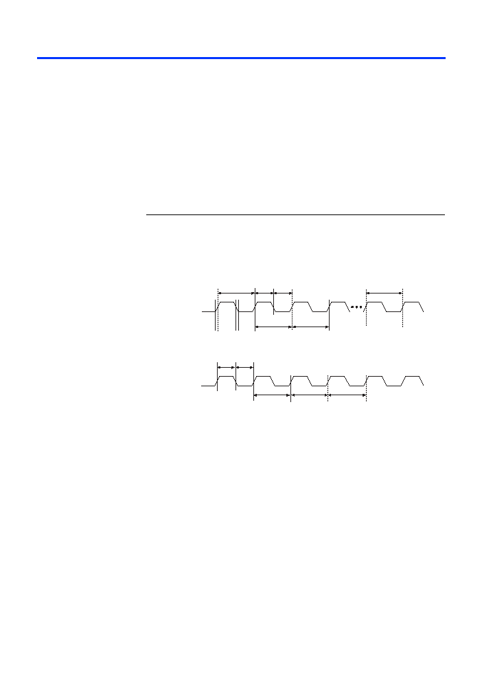
ClockLock & ClockBoost Timing Parameters
For the ClockLock and ClockBoost circuitry to function properly, the
incoming clock must meet certain requirements. If these specifications are
not met, the circuitry may not lock onto the incoming clock, which
generates an erroneous clock within the device. The clock generated by
the ClockLock and ClockBoost circuitry must also meet certain
specifications. If the incoming clock meets these requirements during
configuration, the ClockLock and ClockBoost circuitry will lock onto the
clock during configuration. The circuit will be ready for use immediately
after configuration.
Figure 19
shows the incoming and generated clock
specifications.
Figure 19. Specifications for Incoming & Generated Clocks
The t
I
parameter refers to the nominal input clock period; the t
O
parameter refers to the
nominal output clock period.
t
R
t
F
t
CLK1
t
INDUTY
t
I
±
f
CLKDEV
t
I
t
I
±
t
INCLKSTB
t
OUTDUTY
t
O
t
O +
t
JITTER
t
O ≠
t
JITTER
Input
Clock
ClockLock-
Generated
Clock
40
Altera Corporation
FLEX 10KE Embedded Programmable Logic Devices Data Sheet
Tables 12
and
13
summarize the ClockLock and ClockBoost parameters
for -1 and -2 speed-grade devices, respectively.
Table 12. ClockLock & ClockBoost Parameters for -1 Speed-Grade Devices
Symbol
Parameter
Condition
Min
Typ
Max
Unit
t
R
Input rise time
5
ns
t
F
Input fall time
5
ns
t
INDUTY
Input duty cycle
40
60
%
f
CLK1
Input clock frequency (ClockBoost
clock multiplication factor equals 1)
25
180
MHz
f
CLK2
Input clock frequency (ClockBoost
clock multiplication factor equals 2)
16
90
MHz
f
CLKDEV
Input deviation from user
specification in the MAX+PLUS II
software
(1)
25,000
(2)
PPM
t
INCLKSTB
Input clock stability (measured
between adjacent clocks)
100
ps
t
LOCK
Time required for ClockLock or
ClockBoost to acquire lock
(3)
10
µs
t
JITTER
Jitter on ClockLock or ClockBoost-
generated clock
(4)
t
INCLKSTB
< 100
250
ps
t
INCLKSTB
< 50
200
(4)
ps
t
OUTDUTY
Duty cycle for ClockLock or
ClockBoost-generated clock
40
50
60
%
Altera Corporation
41
FLEX 10KE Embedded Programmable Logic Devices Data Sheet
Notes to tables:
(1)
To implement the ClockLock and ClockBoost circuitry with the MAX+PLUS II software, designers must specify the
input frequency. The Altera software tunes the PLL in the ClockLock and ClockBoost circuitry to this frequency.
The f
CLKDEV
parameter specifies how much the incoming clock can differ from the specified frequency during
device operation. Simulation does not reflect this parameter.
(2)
Twenty-five thousand parts per million (PPM) equates to 2.5% of input clock period.
(3)
During device configuration, the ClockLock and ClockBoost circuitry is configured before the rest of the device. If
the incoming clock is supplied during configuration, the ClockLock and ClockBoost circuitry locks during
configuration because the t
LOCK
value is less than the time required for configuration.
(4)
The t
JITTER
specification is measured under long-term observation. The maximum value for t
JITTER
is 200 ps if
t
INCLKSTB
is lower than 50 ps.
I/O
Configuration
This section discusses the peripheral component interconnect (PCI)
pull-up clamping diode option, slew-rate control, open-drain output
option, and MultiVolt I/O interface for FLEX 10KE devices. The PCI
pull-up clamping diode, slew-rate control, and open-drain output options
are controlled pin-by-pin via Altera software logic options. The MultiVolt
I/O interface is controlled by connecting V
CCIO
to a different voltage than
V
CCINT
. Its effect can be simulated in the Altera software via the Global
Project Device Options
dialog box (Assign menu).
Table 13. ClockLock & ClockBoost Parameters for -2 Speed-Grade Devices
Symbol
Parameter
Condition
Min
Typ
Max
Unit
t
R
Input rise time
5
ns
t
F
Input fall time
5
ns
t
INDUTY
Input duty cycle
40
60
%
f
CLK1
Input clock frequency (ClockBoost
clock multiplication factor equals 1)
25
75
MHz
f
CLK2
Input clock frequency (ClockBoost
clock multiplication factor equals 2)
16
37.5
MHz
f
CLKDEV
Input deviation from user
specification in the MAX+PLUS II
software
(1)
25,000
(2)
PPM
t
INCLKSTB
Input clock stability (measured
between adjacent clocks)
100
ps
t
LOCK
Time required for ClockLock or
ClockBoost to acquire lock
(3)
10
µs
t
JITTER
Jitter on ClockLock or ClockBoost-
generated clock
(4)
t
INCLKSTB
< 100
250
ps
t
INCLKSTB
< 50
200
(4)
ps
t
OUTDUTY
Duty cycle for ClockLock or
ClockBoost-generated clock
40
50
60
%

42
Altera Corporation
FLEX 10KE Embedded Programmable Logic Devices Data Sheet
PCI Pull-Up Clamping Diode Option
FLEX 10KE devices have a pull-up clamping diode on every I/O,
dedicated input, and dedicated clock pin. PCI clamping diodes clamp the
signal to the V
CCIO
value and are required for 3.3-V PCI compliance.
Clamping diodes can also be used to limit overshoot in other systems.
Clamping diodes are controlled on a pin-by-pin basis. When V
CCIO
is
3.3 V, a pin that has the clamping diode option turned on can be driven by
a 2.5-V or 3.3-V signal, but not a 5.0-V signal. When V
CCIO
is 2.5 V, a pin
that has the clamping diode option turned on can be driven by a 2.5-V
signal, but not a 3.3-V or 5.0-V signal. Additionally, a clamping diode can
be activated for a subset of pins, which would allow a device to bridge
between a 3.3-V PCI bus and a 5.0-V device.
Slew-Rate Control
The output buffer in each IOE has an adjustable output slew rate that can
be configured for low-noise or high-speed performance. A slower slew
rate reduces system noise and adds a maximum delay of 4.3 ns. The fast
slew rate should be used for speed-critical outputs in systems that are
adequately protected against noise. Designers can specify the slew rate
pin-by-pin or assign a default slew rate to all pins on a device-wide basis.
The slow slew rate setting affects the falling edge of the output.
Open-Drain Output Option
FLEX 10KE devices provide an optional open-drain output (electrically
equivalent to open-collector output) for each I/O pin. This open-drain
output enables the device to provide system-level control signals (e.g.,
interrupt and write enable signals) that can be asserted by any of several
devices. It can also provide an additional wired-
OR
plane.
MultiVolt I/O Interface
The FLEX 10KE device architecture supports the MultiVolt I/O interface
feature, which allows FLEX 10KE devices in all packages to interface with
systems of differing supply voltages. These devices have one set of V
CC
pins for internal operation and input buffers (
VCCINT
), and another set for
I/O output drivers (
VCCIO
).

Altera Corporation
43
FLEX 10KE Embedded Programmable Logic Devices Data Sheet
The
VCCINT
pins must always be connected to a 2.5-V power supply.
With a 2.5-V V
CCINT
level, input voltages are compatible with 2.5-V, 3.3-
V, and 5.0-V inputs. The
VCCIO
pins can be connected to either a 2.5-V or
3.3-V power supply, depending on the output requirements. When the
VCCIO
pins are connected to a 2.5-V power supply, the output levels are
compatible with 2.5-V systems. When the
VCCIO
pins are connected to a
3.3-V power supply, the output high is at 3.3 V and is therefore compatible
with 3.3-V or 5.0-V systems. Devices operating with V
CCIO
levels higher
than 3.0 V achieve a faster timing delay of t
OD2
instead of t
OD1
.
Table 14
summarizes FLEX 10KE MultiVolt I/O support.
Notes:
(1)
The PCI clamping diode must be disabled to drive an input with voltages higher
than V
CCIO
.
(2)
When V
CCIO
= 3.3 V, a FLEX 10KE device can drive a 2.5-V device that has 3.3-V
tolerant inputs.
Open-drain output pins on FLEX 10KE devices (with a pull-up resistor to
the 5.0-V supply) can drive 5.0-V CMOS input pins that require a V
IH
of
3.5 V. When the open-drain pin is active, it will drive low. When the pin is
inactive, the trace will be pulled up to 5.0 V by the resistor. The open-drain
pin will only drive low or tri-state; it will never drive high. The rise time
is dependent on the value of the pull-up resistor and load impedance. The
I
OL
current specification should be considered when selecting a pull-up
resistor.
Power Sequencing & Hot-Socketing
Because FLEX 10KE devices can be used in a mixed-voltage environment,
they have been designed specifically to tolerate any possible power-up
sequence. The V
CCIO
and V
CCINT
power planes can be powered in any
order.
Signals can be driven into FLEX 10KE devices before and during power
up without damaging the device. Additionally, FLEX 10KE devices do not
drive out during power up. Once operating conditions are reached,
FLEX 10KE devices operate as specified by the user.
Table 14. FLEX 10KE MultiVolt I/O Support
V
CCIO
(V)
Input Signal (V)
Output Signal (V)
2.5
3.3
5.0
2.5
3.3
5.0
2.5
v
v
(1)
v
(1)
v
3.3
v
v
v
(1)
v
(2)
v
v
44
Altera Corporation
FLEX 10KE Embedded Programmable Logic Devices Data Sheet
IEEE Std.
1149.1 (JTAG)
Boundary-Scan
Support
All FLEX 10KE devices provide JTAG BST circuitry that complies with the
IEEE Std. 1149.1-1990 specification. FLEX 10KE devices can also be
configured using the JTAG pins through the BitBlaster or ByteBlasterMV
download cable, or via hardware that uses the Jam
TM
STAPL
programming and test language. JTAG boundary-scan testing can be
performed before or after configuration, but not during configuration.
FLEX 10KE devices support the JTAG instructions shown in
Table 15
.
The instruction register length of FLEX 10KE devices is 10 bits. The
USERCODE register length in FLEX 10KE devices is 32 bits; 7 bits are
determined by the user, and 25 bits are pre-determined.
Tables 16
and
17
show the boundary-scan register length and device IDCODE information
for FLEX 10KE devices.
Table 15. FLEX 10KE JTAG Instructions
JTAG Instruction
Description
SAMPLE/PRELOAD
Allows a snapshot of signals at the device pins to be captured and examined during
normal device operation, and permits an initial data pattern to be output at the device
pins.
EXTEST
Allows the external circuitry and board-level interconnections to be tested by forcing a
test pattern at the output pins and capturing test results at the input pins.
BYPASS
Places the 1-bit bypass register between the
TDI
and
TDO
pins, which allows the BST
data to pass synchronously through a selected device to adjacent devices during normal
device operation.
USERCODE
Selects the user electronic signature (USERCODE) register and places it between the
TDI
and
TDO
pins, allowing the USERCODE to be serially shifted out of
TDO
.
IDCODE
Selects the IDCODE register and places it between
TDI
and
TDO
, allowing the IDCODE
to be serially shifted out of
TDO
.
ICR Instructions
These instructions are used when configuring a FLEX 10KE device via JTAG ports with
a BitBlaster or ByteBlasterMV download cable, or using a Jam File (.jam) or
Jam Byte-Code File (.jbc) via an embedded processor.
Table 16. FLEX 10KE Boundary-Scan Register Length
Device
Boundary-Scan Register Length
EPF10K30E
690
EPF10K50E
EPF10K50S
798
EPF10K100E
1,050
EPF10K130E
1,308
EPF10K200E
EPF10K200S
1,446

Altera Corporation
45
FLEX 10KE Embedded Programmable Logic Devices Data Sheet
Notes:
(1)
The most significant bit (MSB) is on the left.
(2)
The least significant bit (LSB) for all JTAG IDCODEs is
1
.
FLEX 10KE devices include weak pull-up resistors on the JTAG pins.
f
For more information, see the following documents:
Application Note 39 (IEEE Std. 1149.1 (JTAG) Boundary-Scan Testing in
Altera Devices)
BitBlaster Serial Download Cable Data Sheet
ByteBlasterMV Parallel Port Download Cable Data Sheet
Jam Programming & Test Language Specification
Table 17. 32-Bit IDCODE for FLEX 10KE Devices
Note (1)
Device
IDCODE (32 Bits)
Version
(4 Bits)
Part Number (16 Bits)
Manufacturer's
Identity (11 Bits)
1 (1 Bit)
(2)
EPF10K30E
0001
0001 0000 0011 0000
00001101110
1
EPF10K50E
EPF10K50S
0001
0001 0000 0101 0000
00001101110
1
EPF10K100E
0010
0000 0001 0000 0000
00001101110
1
EPF10K130E
0001
0000 0001 0011 0000
00001101110
1
EPF10K200E
EPF10K200S
0001
0000 0010 0000 0000
00001101110
1

46
Altera Corporation
FLEX 10KE Embedded Programmable Logic Devices Data Sheet
Figure 20
shows the timing requirements for the JTAG signals.
Figure 20. FLEX 10KE JTAG Waveforms
Table 18
shows the timing parameters and values for FLEX 10KE devices.
Table 18. FLEX 10KE JTAG Timing Parameters & Values
Symbol
Parameter
Min
Max
Unit
t
JCP
TCK
clock period
100
ns
t
JCH
TCK
clock high time
50
ns
t
JCL
TCK
clock low time
50
ns
t
JPSU
JTAG port setup time
20
ns
t
JPH
JTAG port hold time
45
ns
t
JPCO
JTAG port clock to output
25
ns
t
JPZX
JTAG port high impedance to valid output
25
ns
t
JPXZ
JTAG port valid output to high impedance
25
ns
t
JSSU
Capture register setup time
20
ns
t
JSH
Capture register hold time
45
ns
t
JSCO
Update register clock to output
35
ns
t
JSZX
Update register high impedance to valid output
35
ns
t
JSXZ
Update register valid output to high impedance
35
ns
TDO
TCK
t
JPZX
t
JPCO
t
JPH
t
JPXZ
t
JCP
t
JPSU
t
JCL
t
JCH
TDI
TMS
Signal
to Be
Captured
Signal
to Be
Driven
t
JSZX
t
JSSU
t
JSH
t
JSCO
t
JSXZ

Altera Corporation
47
FLEX 10KE Embedded Programmable Logic Devices Data Sheet
Generic Testing
Each FLEX 10KE device is functionally tested. Complete testing of each
configurable static random access memory (SRAM) bit and all logic
functionality ensures 100% yield. AC test measurements for FLEX 10KE
devices are made under conditions equivalent to those shown in
Figure 21
. Multiple test patterns can be used to configure devices during
all stages of the production flow.
Figure 21. FLEX 10KE AC Test Conditions
Operating
Conditions
Tables 19
through
23
provide information on absolute maximum ratings,
recommended operating conditions, DC operating conditions, and
capacitance for 2.5-V FLEX 10KE devices.
Test
System
C1 (includes
JIG capacitance)
Device input
rise and fall
times < 3 ns
Device
Output
703
8.06 k
[481 ]
[481 ]
VCCIO
Power supply transients can affect AC
measurements. Simultaneous transitions of
multiple outputs should be avoided for
accurate measurement. Threshold tests
must not be performed under AC
conditions. Large-amplitude, fast-ground-
current transients normally occur as the
device outputs discharge the load
capacitances. When these transients flow
through the parasitic inductance between
the device ground pin and the test system
ground, significant reductions in
observable noise immunity can result.
Numbers in brackets are for 2.5-V devices
or outputs. Numbers without brackets are
for 3.3-V. devices or outputs.
Table 19. FLEX 10KE 2.5-V Device Absolute Maximum Ratings
Note (1)
Symbol
Parameter
Conditions
Min
Max
Unit
V
CCINT
Supply voltage
With respect to ground
(2)
≠0.5
3.6
V
V
CCIO
≠0.5
4.6
V
V
I
DC input voltage
≠2.0
5.75
V
I
OUT
DC output current, per pin
≠25
25
mA
T
STG
Storage temperature
No bias
≠65
150
∞ C
T
AMB
Ambient temperature
Under bias
≠65
135
∞ C
T
J
Junction temperature
PQFP, TQFP, BGA, and FineLine BGA
packages, under bias
135
∞ C
Ceramic PGA packages, under bias
150
∞ C
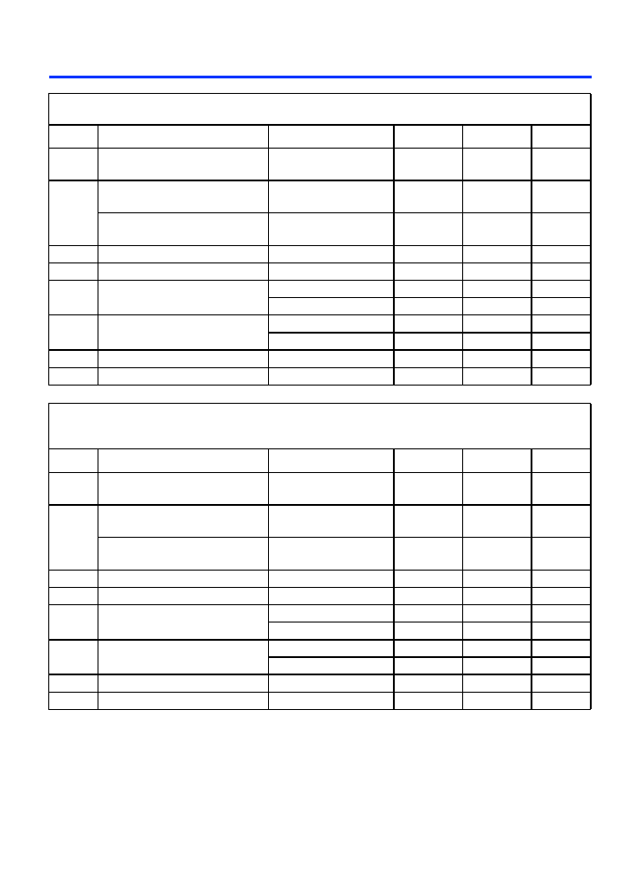
48
Altera Corporation
FLEX 10KE Embedded Programmable Logic Devices Data Sheet
Table 20. 2.5-V EPF10K50E & EPF10K200E Device Recommended Operating Conditions
Symbol
Parameter
Conditions
Min
Max
Unit
V
CCINT
Supply voltage for internal logic
and input buffers
(3)
,
(4)
2.30 (2.30)
2.70 (2.70)
V
V
CCIO
Supply voltage for output buffers,
3.3-V operation
(3)
,
(4)
3.00 (3.00)
3.60 (3.60)
V
Supply voltage for output buffers,
2.5-V operation
(3)
,
(4)
2.30 (2.30)
2.70 (2.70)
V
V
I
Input voltage
(5)
≠0.5
5.75
V
V
O
Output voltage
0
V
CCIO
V
T
A
Ambient temperature
For commercial use
0
70
∞ C
For industrial use
≠40
85
∞ C
T
J
Operating temperature
For commercial use
0
85
∞ C
For industrial use
≠40
100
∞ C
t
R
Input rise time
40
ns
t
F
Input fall time
40
ns
Table 21. 2.5-V EPF10K30E, EPF10K50S, EPF10K100E, EPF10K130E & EPF10K200S Device
Recommended Operating Conditions
Symbol
Parameter
Conditions
Min
Max
Unit
V
CCINT
Supply voltage for internal logic
and input buffers
(3)
,
(4)
2.375
(2.375)
2.625
(2.625)
V
V
CCIO
Supply voltage for output buffers,
3.3-V operation
(3)
,
(4)
3.00 (3.00)
3.60 (3.60)
V
Supply voltage for output buffers,
2.5-V operation
(3)
,
(4)
2.375
(2.375)
2.625
(2.625)
V
V
I
Input voltage
(5)
≠0.5
5.75
V
V
O
Output voltage
0
V
CCIO
V
T
A
Ambient temperature
For commercial use
0
70
∞ C
For industrial use
≠40
85
∞ C
T
J
Operating temperature
For commercial use
0
85
∞ C
For industrial use
≠40
100
∞ C
t
R
Input rise time
40
ns
t
F
Input fall time
40
ns

Altera Corporation
49
FLEX 10KE Embedded Programmable Logic Devices Data Sheet
Table 22. FLEX 10KE 2.5-V Device DC Operating Conditions
Notes (6)
,
(7)
Symbol
Parameter
Conditions
Min
Typ
Max
Unit
V
IH
High-level input
voltage
1.7, 0.5
◊
V
CCIO
(8)
5.75
V
V
IL
Low-level input
voltage
≠0.5
0.8,
0.3
◊
V
CCIO
(8)
V
V
OH
3.3-V high-level TTL
output voltage
I
OH
= ≠8 mA DC,
V
CCIO
= 3.00 V
(9)
2.4
V
3.3-V high-level
CMOS output voltage
I
OH
= ≠0.1 mA DC,
V
CCIO
= 3.00 V
(9)
V
CCIO
≠ 0.2
V
3.3-V high-level PCI
output voltage
I
OH
= ≠0.5 mA DC,
V
CCIO
= 3.00 to 3.60 V
(9)
0.9
◊
V
CCIO
V
2.5-V high-level output
voltage
I
OH
= ≠0.1 mA DC,
V
CCIO
= 2.30 V
(9)
2.1
V
I
OH
= ≠1 mA DC,
V
CCIO
= 2.30 V
(9)
2.0
V
I
OH
= ≠2 mA DC,
V
CCIO
= 2.30 V
(9)
1.7
V
V
OL
3.3-V low-level TTL
output voltage
I
OL
= 12 mA DC,
V
CCIO
= 3.00 V
(10)
0.45
V
3.3-V low-level CMOS
output voltage
I
OL
= 0.1 mA DC,
V
CCIO
= 3.00 V
(10)
0.2
V
3.3-V low-level PCI
output voltage
I
OL
= 1.5 mA DC,
V
CCIO
= 3.00 to 3.60 V
(10)
0.1
◊
V
CCIO
V
2.5-V low-level output
voltage
I
OL
= 0.1 mA DC,
V
CCIO
= 2.30 V
(10)
0.2
V
I
OL
= 1 mA DC,
V
CCIO
= 2.30 V
(10)
0.4
V
I
OL
= 2 mA DC,
V
CCIO
= 2.30 V
(10)
0.7
V
I
I
Input pin leakage
current
V
I
= V
CCIOmax
to 0 V
(11)
≠10
10
µ
A
I
OZ
Tri-stated I/O pin
leakage current
V
O
= V
CCIOmax
to 0 V
(11)
≠10
10
µ
A
I
CC0
V
CC
supply current
(standby)
V
I
= ground, no load, no
toggling inputs
5
mA
V
I
= ground, no load, no
toggling inputs
(12)
10
mA
R
CONF
Value of I/O pin pull-
up resistor before and
during configuration
V
CCIO
= 3.0 V
(13)
20
50
kæ
V
CCIO
= 2.3 V
(13)
30
80
kæ

50
Altera Corporation
FLEX 10KE Embedded Programmable Logic Devices Data Sheet
Notes to tables:
(1)
See the
Operating Requirements for Altera Devices Data Sheet
.
(2)
Minimum DC input voltage is ≠0.5 V. During transitions, the inputs may undershoot to ≠2.0 V for input currents
less than 100 mA and periods shorter than 20 ns.
(3)
Numbers in parentheses are for industrial-temperature-range devices.
(4)
Maximum V
CC
rise time is 100 ms, and V
CC
must rise monotonically.
(5)
All pins, including dedicated inputs, clock, I/O, and JTAG pins, may be driven before V
CCINT
and V
CCIO
are
powered.
(6)
Typical values are for T
A
= 25
∞
C, V
CCINT
= 2.5 V, and V
CCIO
= 2.5 V or 3.3 V.
(7)
These values are specified under the FLEX 10KE Recommended Operating Conditions shown in
Tables 20
and
21
.
(8)
The FLEX 10KE input buffers are compatible with 2.5-V, 3.3-V (LVTTL and LVCMOS), and 5.0-V TTL and CMOS
signals. Additionally, the input buffers are 3.3-V PCI compliant when
V
CCIO
and V
CCINT
meet the relationship shown
in
Figure 22
.
(9)
The I
OH
parameter refers to high-level TTL, PCI, or CMOS output current.
(10) The I
OL
parameter refers to low-level TTL, PCI, or CMOS output current. This parameter applies to open-drain pins
as well as output pins.
(11) This value is specified for normal device operation. The value may vary during power-up.
(12) This parameter applies to -1 speed-grade commercial-temperature devices and -2 speed-grade-industrial
temperature devices.
(13) Pin pull-up resistance values will be lower if the pin is driven higher than V
CCIO
by an external source.
(14) Capacitance is sample-tested only.
Table 23. FLEX 10KE Device Capacitance
Note (14)
Symbol
Parameter
Conditions
Min
Max
Unit
C
IN
Input capacitance
V
IN
= 0 V, f = 1.0 MHz
10
pF
C
INCLK
Input capacitance on
dedicated clock pin
V
IN
= 0 V, f = 1.0 MHz
12
pF
C
OUT
Output capacitance
V
OUT
= 0 V, f = 1.0 MHz
10
pF

Altera Corporation
51
FLEX 10KE Embedded Programmable Logic Devices Data Sheet
Figure 22
shows the required relationship between V
CCIO
and V
CCINT
for
3.3-V PCI compliance.
Figure 22. Relationship between V
CCIO
& V
CCINT
for 3.3-V PCI Compliance
Figure 23
shows the typical output drive characteristics of FLEX 10KE
devices with 3.3-V and 2.5-V V
CCIO
. The output driver is compliant to the
3.3-V
PCI Local Bus Specification
, Revision 2.2
(when
VCCIO
pins are
connected to 3.3 V). FLEX 10KE devices with a -1 speed grade also comply
with the drive strength requirements of the
PCI Local Bus Specification
,
Revision 2.2
(when
VCCINT
pins are powered with a minimum supply of
2.375 V, and
VCCIO
pins are connected to 3.3 V). Therefore, these devices
can be used in open 5.0-V PCI systems.
3.0
3.1
3.3
V
CCIO
IO
3.6
2.3
2.5
2.7
V
CCINT
II
(V)
(V)
PCI-Compliant Region

52
Altera Corporation
FLEX 10KE Embedded Programmable Logic Devices Data Sheet
Figure 23. Output Drive Characteristics of FLEX 10KE Devices
Note (1)
Note:
(1)
These are transient (AC) currents.
Timing Model
The continuous, high-performance FastTrack Interconnect routing
resources ensure predictable performance and accurate simulation and
timing analysis. This predictable performance contrasts with that of
FPGAs, which use a segmented connection scheme and therefore have
unpredictable performance.
Device performance can be estimated by following the signal path from a
source, through the interconnect, to the destination. For example, the
registered performance between two LEs on the same row can be
calculated by adding the following parameters:
LE register clock-to-output delay (t
CO
)
Interconnect delay (t
SAMEROW
)
LE look-up table delay (t
LUT
)
LE register setup time (t
SU
)
The routing delay depends on the placement of the source and destination
LEs. A more complex registered path may involve multiple combinatorial
LEs between the source and destination LEs.
V
O
Output Voltage (V)
I
OL
I
OH
I
OH
V
V
V
CCINT
= 2.5
V
CCIO
= 2.5
Room Temperature
V
V
V
CCINT
= 2.5
V
CCIO
= 3.3
Room Temperature
1
2
3
10
20
30
50
60
40
70
80
90
V
O
Output Voltage (V)
1
2
3
10
20
30
50
60
40
70
80
90
I
OL
O
Typical I
Output
Current (mA)
O
Typical I
Output
Current (mA)

Altera Corporation
53
FLEX 10KE Embedded Programmable Logic Devices Data Sheet
Timing simulation and delay prediction are available with the Altera
Simulator and Timing Analyzer, or with industry-standard EDA tools.
The Simulator offers both pre-synthesis functional simulation to evaluate
logic design accuracy and post-synthesis timing simulation with 0.1-ns
resolution. The Timing Analyzer provides point-to-point timing delay
information, setup and hold time analysis, and device-wide performance
analysis.
Figure 24
shows the overall timing model, which maps the possible paths
to and from the various elements of the FLEX 10KE device.
Figure 24. FLEX 10KE Device Timing Model
Figures 25
through
28
show the delays that correspond to various paths
and functions within the LE, IOE, EAB, and bidirectional timing models.
Dedicated
Clock/Input
Interconnect
I/O Element
Logic
Element
Embedded Array
Block

54
Altera Corporation
FLEX 10KE Embedded Programmable Logic Devices Data Sheet
Figure 25. FLEX 10KE Device LE Timing Model
t
CGENR
t
CO
t
COMB
t
SU
t
H
t
PRE
t
CLR
Register
Delays
LUT Delay
t
LUT
t
RLUT
t
CLUT
Carry Chain
Delay
Carry-In
Cascade-In
Data-Out
t
CGEN
t
CICO
Packed Register
Delay
t
PACKED
Register Control
Delay
t
C
t
EN
Data-In
Control-In
t
CASC
Cascade-Out
Carry-Out
t
LABCARRY
t
LABCASC

Altera Corporation
55
FLEX 10KE Embedded Programmable Logic Devices Data Sheet
Figure 26. FLEX 10KE Device IOE Timing Model
Figure 27. FLEX 10KE Device EAB Timing Model
Data-In
I/O Register
Delays
t
IOCO
t
IOCOMB
t
IOSU
t
IOH
t
IOCLR
Output Data
Delay
t
IOD
I/O Element
Contol Delay
t
IOC
Input Register Delay
t
INREG
Output
Delays
t
OD1
t
OD2
t
OD3
t
XZ
t
ZX1
t
ZX2
t
ZX3
I/O Register
Feedback Delay
t
IOFD
Input Delay
t
INCOMB
Clock Enable
Clear
Data Feedback
into FastTrack
Interconnect
Clock
Output Enable
EAB Data Input
Delays
t
EABDATA1
t
EABDATA2
Data-In
Write Enable
Input Delays
t
EABWE1
t
EABWE2
EAB Clock
Delay
t
EABCLK
Input Register
Delays
t
EABCO
t
EABBYPASS
t
EABSU
t
EABH
t
EABCH
t
EABCL
t
EABRE1
t
EABRE2
RAM/ROM
Block Delays
t
AA
t
RP
t
RASU
t
RAH
t
DD
t
WP
t
WDSU
t
WDH
t
WASU
t
WAH
t
WO
Output Register
Delays
t
EABCO
t
EABBYPASS
t
EABSU
t
EABH
t
EABCH
t
EABCL
t
EABOUT
Address
WE
Input Register
Clock
Output Register
Clock
Data-Out
EAB Output
Delay
Read Enable
Input Delays
RE

56
Altera Corporation
FLEX 10KE Embedded Programmable Logic Devices Data Sheet
Figure 28. Synchronous Bidirectional Pin External Timing Model
Tables 24
through
28
describe the FLEX 10KE device internal timing
parameters.
Tables 29
through
30
describe the FLEX 10KE external timing
parameters and their symbols.
PRN
CLRN
D
Q
PRN
CLRN
D
Q
PRN
CLRN
D
Q
Dedicated
Clock
Bidirectional
Pin
Output Register
t
INSUBIDIR
t
OUTCOBIDIR
t
XZBIDIR
t
ZXBIDIR
t
INHBIDIR
OE Register
Input Register
Table 24. LE Timing Microparameters (Part 1 of 2)
Note (1)
Symbol
Parameter
Condition
t
LUT
LUT delay for data-in
t
CLUT
LUT delay for carry-in
t
RLUT
LUT delay for LE register feedback
t
PACKED
Data-in to packed register delay
t
EN
LE register enable delay
t
CICO
Carry-in to carry-out delay
t
CGEN
Data-in to carry-out delay
t
CGENR
LE register feedback to carry-out delay
t
CASC
Cascade-in to cascade-out delay
t
C
LE register control signal delay
t
CO
LE register clock-to-output delay
t
COMB
Combinatorial delay
t
SU
LE register setup time for data and enable signals before clock; LE register
recovery time after asynchronous clear, preset, or load
t
H
LE register hold time for data and enable signals after clock
t
PRE
LE register preset delay

Altera Corporation
57
FLEX 10KE Embedded Programmable Logic Devices Data Sheet
t
CLR
LE register clear delay
t
CH
Minimum clock high time from clock pin
t
CL
Minimum clock low time from clock pin
Table 24. LE Timing Microparameters (Part 2 of 2)
Note (1)
Symbol
Parameter
Condition
Table 25. IOE Timing Microparameters
Note (1)
Symbol
Parameter
Conditions
t
IOD
IOE data delay
t
IOC
IOE register control signal delay
t
IOCO
IOE register clock-to-output delay
t
IOCOMB
IOE combinatorial delay
t
IOSU
IOE register setup time for data and enable signals before clock; IOE register
recovery time after asynchronous clear
t
IOH
IOE register hold time for data and enable signals after clock
t
IOCLR
IOE register clear time
t
OD1
Output buffer and pad delay, slow slew rate = off, V
CCIO
= 3.3 V
C1 = 35 pF
(2)
t
OD2
Output buffer and pad delay, slow slew rate = off, V
CCIO
= 2.5 V
C1 = 35 pF
(3)
t
OD3
Output buffer and pad delay, slow slew rate = on
C1 = 35 pF
(4)
t
XZ
IOE output buffer disable delay
t
ZX1
IOE output buffer enable delay, slow slew rate = off, V
CCIO
= 3.3 V
C1 = 35 pF
(2)
t
ZX2
IOE output buffer enable delay, slow slew rate = off, V
CCIO
= 2.5 V
C1 = 35 pF
(3)
t
ZX3
IOE output buffer enable delay, slow slew rate = on
C1 = 35 pF
(4)
t
INREG
IOE input pad and buffer to IOE register delay
t
IOFD
IOE register feedback delay
t
INCOMB
IOE input pad and buffer to FastTrack Interconnect delay

58
Altera Corporation
FLEX 10KE Embedded Programmable Logic Devices Data Sheet
Table 26. EAB Timing Microparameters
Note (1)
Symbol
Parameter
Conditions
t
EABDATA1
Data or address delay to EAB for combinatorial input
t
EABDATA2
Data or address delay to EAB for registered input
t
EABWE1
Write enable delay to EAB for combinatorial input
t
EABWE2
Write enable delay to EAB for registered input
t
EABRE1
Read enable delay to EAB for combinatorial input
t
EABRE2
Read enable delay to EAB for registered input
t
EABCLK
EAB register clock delay
t
EABCO
EAB register clock-to-output delay
t
EABBYPASS
Bypass register delay
t
EABSU
EAB register setup time before clock
t
EABH
EAB register hold time after clock
t
EABCLR
EAB register asynchronous clear time to output delay
t
AA
Address access delay (including the read enable to output delay)
t
WP
Write pulse width
t
RP
Read pulse width
t
WDSU
Data setup time before falling edge of write pulse
(5)
t
WDH
Data hold time after falling edge of write pulse
(5)
t
WASU
Address setup time before rising edge of write pulse
(5)
t
WAH
Address hold time after falling edge of write pulse
(5)
t
RASU
Address setup time with respect to the falling edge of the read enable
t
RAH
Address hold time with respect to the falling edge of the read enable
t
WO
Write enable to data output valid delay
t
DD
Data-in to data-out valid delay
t
EABOUT
Data-out delay
t
EABCH
Clock high time
t
EABCL
Clock low time

Altera Corporation
59
FLEX 10KE Embedded Programmable Logic Devices Data Sheet
Table 27. EAB Timing Macroparameters
Note (1)
,
(6)
Symbol
Parameter
Conditions
t
EABAA
EAB address access delay
t
EABRCCOMB
EAB asynchronous read cycle time
t
EABRCREG
EAB synchronous read cycle time
t
EABWP
EAB write pulse width
t
EABWCCOMB
EAB asynchronous write cycle time
t
EABWCREG
EAB synchronous write cycle time
t
EABDD
EAB data-in to data-out valid delay
t
EABDATACO
EAB clock-to-output delay when using output registers
t
EABDATASU
EAB data/address setup time before clock when using input register
t
EABDATAH
EAB data/address hold time after clock when using input register
t
EABWESU
EAB
WE
setup time before clock when using input register
t
EABWEH
EAB
WE
hold time after clock when using input register
t
EABWDSU
EAB data setup time before falling edge of write pulse when not using input
registers
t
EABWDH
EAB data hold time after falling edge of write pulse when not using input
registers
t
EABWASU
EAB address setup time before rising edge of write pulse when not using
input registers
t
EABWAH
EAB address hold time after falling edge of write pulse when not using input
registers
t
EABWO
EAB write enable to data output valid delay

60
Altera Corporation
FLEX 10KE Embedded Programmable Logic Devices Data Sheet
Table 28. Interconnect Timing Microparameters
Note (1)
Symbol
Parameter
Conditions
t
DIN2IOE
Delay from dedicated input pin to IOE control input
(7)
t
DIN2LE
Delay from dedicated input pin to LE or EAB control input
(7)
t
DCLK2IOE
Delay from dedicated clock pin to IOE clock
(7)
t
DCLK2LE
Delay from dedicated clock pin to LE or EAB clock
(7)
t
DIN2DATA
Delay from dedicated input or clock to LE or EAB data
(7)
t
SAMELAB
Routing delay for an LE driving another LE in the same LAB
t
SAMEROW
Routing delay for a row IOE, LE, or EAB driving a row IOE, LE, or EAB in the
same row
(7)
t
SAMECOLUMN
Routing delay for an LE driving an IOE in the same column
(7)
t
DIFFROW
Routing delay for a column IOE, LE, or EAB driving an LE or EAB in a different
row
(7)
t
TWOROWS
Routing delay for a row IOE or EAB driving an LE or EAB in a different row
(7)
t
LEPERIPH
Routing delay for an LE driving a control signal of an IOE via the peripheral
control bus
(7)
t
LABCARRY
Routing delay for the carry-out signal of an LE driving the carry-in signal of a
different LE in a different LAB
t
LABCASC
Routing delay for the cascade-out signal of an LE driving the cascade-in
signal of a different LE in a different LAB
Table 29. External Timing Parameters
Symbol
Parameter
Conditions
t
DRR
Register-to-register delay via four LEs, three row interconnects, and four local
interconnects
(8)
t
INSU
Setup time with global clock at IOE register
(9)
t
INH
Hold time with global clock at IOE register
(9)
t
OUTCO
Clock-to-output delay with global clock at IOE register
(9)
t
PCISU
Setup time with global clock for registers used in PCI designs
(9)
,
(10)
t
PCIH
Hold time with global clock for registers used in PCI designs
(9)
,
(10)
t
PCICO
Clock-to-output delay with global clock for registers used in PCI designs
(9)
,
(10)

Altera Corporation
61
FLEX 10KE Embedded Programmable Logic Devices Data Sheet
Notes to tables:
(1)
Microparameters are timing delays contributed by individual architectural elements. These parameters cannot be
measured explicitly.
(2)
Operating conditions: VCCIO = 3.3 V ±10% for commercial or industrial use.
(3)
Operating conditions: VCCIO = 2.5 V ±5% for commercial or industrial use in EPF10K30E, EPF10K50S,
EPF10K100E, EPF10K130E, and EPF10K200S devices.
(4)
Operating conditions: VCCIO = 3.3 V.
(5)
Because the RAM in the EAB is self-timed, this parameter can be ignored when the
WE
signal is registered.
(6)
EAB macroparameters are internal parameters that can simplify predicting the behavior of an EAB at its boundary;
these parameters are calculated by summing selected microparameters.
(7)
These parameters are worst-case values for typical applications. Post-compilation timing simulation and timing
analysis are required to determine actual worst-case performance.
(8)
Contact Altera Applications for test circuit specifications and test conditions.
(9)
This timing parameter is sample-tested only.
(10) This parameter is measured with the measurement and test conditions, including load, specified in the PCI Local
Bus Specification, revision 2.2.
Table 30. External Bidirectional Timing Parameters
Note (9)
Symbol
Parameter
Conditions
t
INSUBIDIR
Setup time for bi-directional pins with global clock at same-row or same-
column LE register
t
INHBIDIR
Hold time for bidirectional pins with global clock at same-row or same-column
LE register
t
INH
Hold time with global clock at IOE register
t
OUTCOBIDIR
Clock-to-output delay for bidirectional pins with global clock at IOE register
C1 = 35 pF
t
XZBIDIR
Synchronous IOE output buffer disable delay
C1 = 35 pF
t
ZXBIDIR
Synchronous IOE output buffer enable delay, slow slew rate= off
C1 = 35 pF
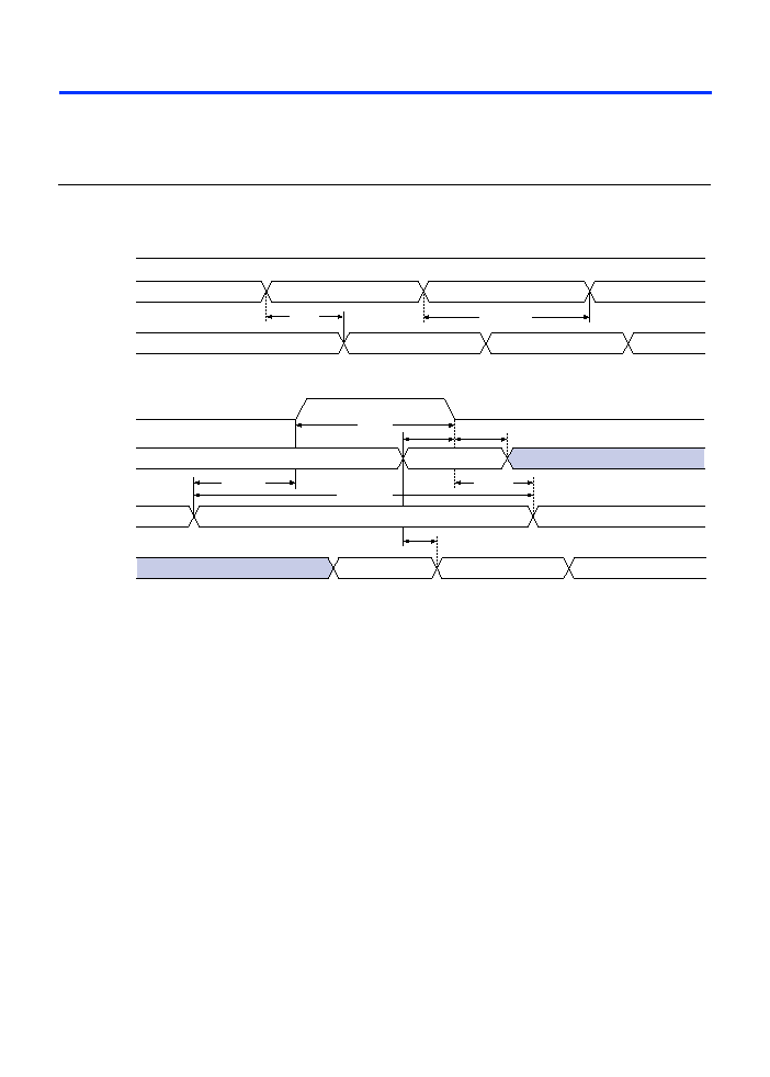
62
Altera Corporation
FLEX 10KE Embedded Programmable Logic Devices Data Sheet
Figures 29
and
30
show the asynchronous and synchronous timing
waveforms, respectively, or the EAB macroparameters in
Tables 26
and
27
.
Figure 29. EAB Asynchronous Timing Waveforms
EAB Asynchronous Write
EAB Asynchronous Read
WE
a0
d0
d3
t
EABRCCOMB
a1
a2
a3
d2
t
EABAA
d1
Address
Data-Out
WE
a0
din1
dout2
t
EABDD
a1
a2
din1
din0
t
EABWCCOMB
t
EABWASU
t
EABWAH
t
EABWDH
t
EABWDSU
t
EABWP
din0
Data-In
Address
Data-Out

Altera Corporation
63
FLEX 10KE Embedded Programmable Logic Devices Data Sheet
Figure 30. EAB Synchronous Timing Waveforms
Tables 31
through
37
show EPF10K30E device internal and external
timing parameters.
WE
CLK
EAB Synchronous Read
a0
d2
t
EABDATASU
t
EABRCREG
t
EABDATACO
a1
a2
a3
d1
t
EABDATAH
a0
WE
CLK
dout0
din1
din2
din3
din2
t
EABWESU
t
EABWCREG
t
EABWEH
t
EABDATACO
a1
a2
a3
a2
din3
din2
din1
t
EABDATAH
t
EABDATASU
EAB Synchronous Write (EAB Output Registers Used)
dout1
Address
Data-Out
Address
Data-Out
Data-In
Table 31. EPF10K30E Device LE Timing Microparameters (Part 1 of 2)
Note (1)
Symbol
-1 Speed Grade
-2 Speed Grade
-3 Speed Grade
Unit
Min
Max
Min
Max
Min
Max
t
LUT
0.7
0.8
1.1
ns
t
CLUT
0.5
0.6
0.8
ns
t
RLUT
0.6
0.7
1.0
ns
t
PACKED
0.3
0.4
0.5
ns
t
EN
0.6
0.8
1.0
ns
t
CICO
0.1
0.1
0.2
ns
t
CGEN
0.4
0.5
0.7
ns
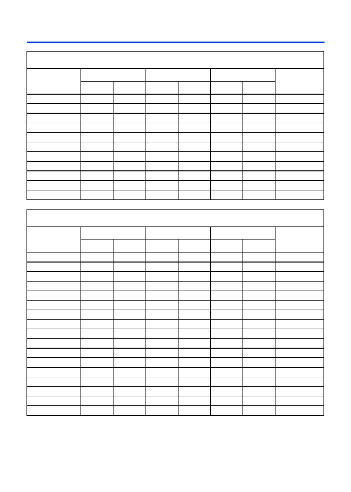
64
Altera Corporation
FLEX 10KE Embedded Programmable Logic Devices Data Sheet
t
CGENR
0.1
0.1
0.2
ns
t
CASC
0.6
0.8
1.0
ns
t
C
0.0
0.0
0.0
ns
t
CO
0.3
0.4
0.5
ns
t
COMB
0.4
0.4
0.6
ns
t
SU
0.4
0.6
0.6
ns
t
H
0.7
1.0
1.3
ns
t
PRE
0.8
0.9
1.2
ns
t
CLR
0.8
0.9
1.2
ns
t
CH
2.0
2.5
2.5
ns
t
CL
2.0
2.5
2.5
ns
Table 32. EPF10K30E Device IOE Timing Microparameters
Note (1)
Symbol
-1 Speed Grade
-2 Speed Grade
-3 Speed Grade
Unit
Min
Max
Min
Max
Min
Max
t
IOD
2.4
2.8
3.8
ns
t
IOC
0.3
0.4
0.5
ns
t
IOCO
1.0
1.1
1.6
ns
t
IOCOMB
0.0
0.0
0.0
ns
t
IOSU
1.2
1.4
1.9
ns
t
IOH
0.3
0.4
0.5
ns
t
IOCLR
1.0
1.1
1.6
ns
t
OD1
1.9
2.3
3.0
ns
t
OD2
1.4
1.8
2.5
ns
t
OD3
4.4
5.2
7.0
ns
t
XZ
2.7
3.1
4.3
ns
t
ZX1
2.7
3.1
4.3
ns
t
ZX2
2.2
2.6
3.8
ns
t
ZX3
5.2
6.0
8.3
ns
t
INREG
3.4
4.1
5.5
ns
t
IOFD
0.8
1.3
2.4
ns
t
INCOMB
0.8
1.3
2.4
ns
Table 31. EPF10K30E Device LE Timing Microparameters (Part 2 of 2)
Note (1)
Symbol
-1 Speed Grade
-2 Speed Grade
-3 Speed Grade
Unit
Min
Max
Min
Max
Min
Max

Altera Corporation
65
FLEX 10KE Embedded Programmable Logic Devices Data Sheet
Table 33. EPF10K30E Device EAB Internal Microparameters
Note (1)
Symbol
-1 Speed Grade
-2 Speed Grade
-3 Speed Grade
Unit
Min
Max
Min
Max
Min
Max
t
EABDATA1
1.7
2.0
2.3
ns
t
EABDATA1
0.6
0.7
0.8
ns
t
EABWE1
1.1
1.3
1.4
ns
t
EABWE2
0.4
0.4
0.5
ns
t
EABRE1
0.8
0.9
1.0
ns
t
EABRE2
0.4
0.4
0.5
ns
t
EABCLK
0.0
0.0
0.0
ns
t
EABCO
0.3
0.3
0.4
ns
t
EABBYPASS
0.5
0.6
0.7
ns
t
EABSU
0.9
1.0
1.2
ns
t
EABH
0.4
0.4
0.5
ns
t
EABCLR
0.3
0.3
0.3
ns
t
AA
3.2
3.8
4.4
ns
t
WP
2.5
2.9
3.3
ns
t
RP
0.9
1.1
1.2
ns
t
WDSU
0.9
1.0
1.1
ns
t
WDH
0.1
0.1
0.1
ns
t
WASU
1.7
2.0
2.3
ns
t
WAH
1.8
2.1
2.4
ns
t
RASU
3.1
3.7
4.2
ns
t
RAH
0.2
0.2
0.2
ns
t
WO
2.5
2.9
3.3
ns
t
DD
2.5
2.9
3.3
ns
t
EABOUT
0.5
0.6
0.7
ns
t
EABCH
1.5
2.0
2.3
ns
t
EABCL
2.5
2.9
3.3
ns

66
Altera Corporation
FLEX 10KE Embedded Programmable Logic Devices Data Sheet
Table 34. EPF10K30E Device EAB Internal Timing Macroparameters
Note (1)
Symbol
-1 Speed Grade
-2 Speed Grade
-3 Speed Grade
Unit
Min
Max
Min
Max
Min
Max
t
EABAA
6.4
7.6
8.8
ns
t
EABRCOMB
6.4
7.6
8.8
ns
t
EABRCREG
4.4
5.1
6.0
ns
t
EABWP
2.5
2.9
3.3
ns
t
EABWCOMB
6.0
7.0
8.0
ns
t
EABWCREG
6.8
7.8
9.0
ns
t
EABDD
5.7
6.7
7.7
ns
t
EABDATACO
0.8
0.9
1.1
ns
t
EABDATASU
1.5
1.7
2.0
ns
t
EABDATAH
0.0
0.0
0.0
ns
t
EABWESU
1.3
1.4
1.7
ns
t
EABWEH
0.0
0.0
0.0
ns
t
EABWDSU
1.5
1.7
2.0
ns
t
EABWDH
0.0
0.0
0.0
ns
t
EABWASU
3.0
3.6
4.3
ns
t
EABWAH
0.5
0.5
0.4
ns
t
EABWO
5.1
6.0
6.8
ns
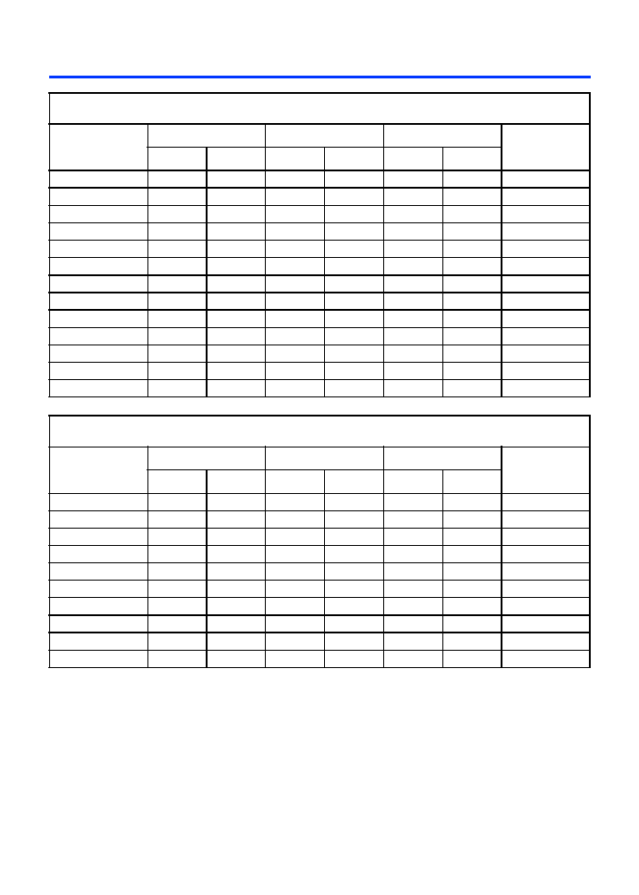
Altera Corporation
67
FLEX 10KE Embedded Programmable Logic Devices Data Sheet
Table 35. EPF10K30E Device Interconnect Timing Microparameters
Note (1)
Symbol
-1 Speed Grade
-2 Speed Grade
-3 Speed Grade
Unit
Min
Max
Min
Max
Min
Max
t
DIN2IOE
1.8
2.4
2.9
ns
t
DIN2LE
1.5
1.8
2.4
ns
t
DIN2DATA
1.5
1.8
2.2
ns
t
DCLK2IOE
2.2
2.6
3.0
ns
t
DCLK2LE
1.5
1.8
2.4
ns
t
SAMELAB
0.1
0.2
0.3
ns
t
SAMEROW
2.0
2.4
2.7
ns
t
SAMECOLUMN
0.7
1.0
0.8
ns
t
DIFFROW
2.7
3.4
3.5
ns
t
TWOROWS
4.7
5.8
6.2
ns
t
LEPERIPH
2.7
3.4
3.8
ns
t
LABCARRY
0.3
0.4
0.5
ns
t
LABCASC
0.8
0.8
1.1
ns
Table 36. EPF10K30E External Timing Parameters
Notes (1)
,
(2)
Symbol
-1 Speed Grade
-2 Speed Grade
-3 Speed Grade
Unit
Min
Max
Min
Max
Min
Max
t
DRR
8.0
9.5
12.5
ns
t
INSU
(3)
2.1
2.5
3.9
ns
t
INH
(3)
0.0
0.0
0.0
ns
t
OUTCO
(3)
2.0
4.9
2.0
5.9
2.0
7.6
ns
t
INSU
(4)
1.1
1.5
≠
ns
t
INH
(4)
0.0
0.0
≠
ns
t
OUTCO
(4)
0.5
3.9
0.5
4.9
≠
≠
ns
t
PCISU
3.0
4.2
≠
ns
t
PCIH
0.0
0.0
≠
ns
t
PCICO
2.0
6.0
2.0
7.5
≠
≠
ns

68
Altera Corporation
FLEX 10KE Embedded Programmable Logic Devices Data Sheet
Notes to tables:
(1)
All timing parameters are described in
Tables 24
through
30
in this data sheet.
(2)
These parameters are specified by characterization.
(3)
This parameter is measured without the use of the ClockLock or ClockBoost circuits.
(4)
This parameter is measured with the use of the ClockLock or ClockBoost circuits.
Tables 38
through
44
show EPF10K50E device internal and external
timing parameters.
Table 37. EPF10K30E External Bidirectional Timing Parameters
Notes (1)
,
(2)
Symbol
-1 Speed Grade
-2 Speed Grade
-3 Speed Grade
Unit
Min
Max
Min
Max
Min
Max
t
INSUBIDIR
(3)
2.8
3.9
5.2
ns
t
INHBIDIR
(3)
0.0
0.0
0.0
ns
t
INSUBIDIR
(4)
3.8
4.9
≠
ns
t
INHBIDIR
(4)
0.0
0.0
≠
ns
t
OUTCOBIDIR
(3)
2.0
4.9
2.0
5.9
2.0
7.6
ns
t
XZBIDIR
(3)
6.1
7.5
9.7
ns
t
ZXBIDIR
(3)
6.1
7.5
9.7
ns
t
OUTCOBIDIR
(4)
0.5
3.9
0.5
4.9
≠
≠
ns
t
XZBIDIR
(4)
5.1
6.5
≠
ns
t
ZXBIDIR
(4)
5.1
6.5
≠
ns
Table 38. EPF10K50E Device LE Timing Microparameters (Part 1 of 2)
Note (1)
Symbol
-1 Speed Grade
-2 Speed Grade
-3 Speed Grade
Unit
Min
Max
Min
Max
Min
Max
t
LUT
0.6
0.9
1.3
ns
t
CLUT
0.5
0.6
0.8
ns
t
RLUT
0.7
0.8
1.1
ns
t
PACKED
0.4
0.5
0.6
ns
t
EN
0.6
0.7
0.9
ns
t
CICO
0.2
0.2
0.3
ns
t
CGEN
0.5
0.5
0.8
ns
t
CGENR
0.2
0.2
0.3
ns
t
CASC
0.8
1.0
1.4
ns
t
C
0.5
0.6
0.8
ns
t
CO
0.7
0.7
0.9
ns
t
COMB
0.5
0.6
0.8
ns
t
SU
0.7
0.7
0.8
ns

Altera Corporation
69
FLEX 10KE Embedded Programmable Logic Devices Data Sheet
t
H
0.9
1.0
1.4
ns
t
PRE
0.5
0.6
0.8
ns
t
CLR
0.5
0.6
0.8
ns
t
CH
2.0
2.5
3.0
ns
t
CL
2.0
2.5
3.0
ns
Table 39. EPF10K50E Device IOE Timing Microparameters
Note (1)
Symbol
-1 Speed Grade
-2 Speed Grade
-3 Speed Grade
Unit
Min
Max
Min
Max
Min
Max
t
IOD
2.2
2.4
3.3
ns
t
IOC
0.3
0.3
0.5
ns
t
IOCO
1.0
1.0
1.4
ns
t
IOCOMB
0.0
0.0
0.2
ns
t
IOSU
1.0
1.2
1.7
ns
t
IOH
0.3
0.3
0.5
ns
t
IOCLR
0.9
1.0
1.4
ns
t
OD1
0.8
0.9
1.2
ns
t
OD2
0.3
0.4
0.7
ns
t
OD3
3.0
3.5
3.5
ns
t
XZ
1.4
1.7
2.3
ns
t
ZX1
1.4
1.7
2.3
ns
t
ZX2
0.9
1.2
1.8
ns
t
ZX3
3.6
4.3
4.6
ns
t
INREG
4.9
5.8
7.8
ns
t
IOFD
2.8
3.3
4.5
ns
t
INCOMB
2.8
3.3
4.5
ns
Table 38. EPF10K50E Device LE Timing Microparameters (Part 2 of 2)
Note (1)
Symbol
-1 Speed Grade
-2 Speed Grade
-3 Speed Grade
Unit
Min
Max
Min
Max
Min
Max

70
Altera Corporation
FLEX 10KE Embedded Programmable Logic Devices Data Sheet
Table 40. EPF10K50E Device EAB Internal Microparameters
Note (1)
Symbol
-1 Speed Grade
-2 Speed Grade
-3 Speed Grade
Unit
Min
Max
Min
Max
Min
Max
t
EABDATA1
1.7
2.0
2.7
ns
t
EABDATA1
0.6
0.7
0.9
ns
t
EABWE1
1.1
1.3
1.8
ns
t
EABWE2
0.4
0.4
0.6
ns
t
EABRE1
0.8
0.9
1.2
ns
t
EABRE2
0.4
0.4
0.6
ns
t
EABCLK
0.0
0.0
0.0
ns
t
EABCO
0.3
0.3
0.5
ns
t
EABBYPASS
0.5
0.6
0.8
ns
t
EABSU
0.9
1.0
1.4
ns
t
EABH
0.4
0.4
0.6
ns
t
EABCLR
0.3
0.3
0.5
ns
t
AA
3.2
3.8
5.1
ns
t
WP
2.5
2.9
3.9
ns
t
RP
0.9
1.1
1.5
ns
t
WDSU
0.9
1.0
1.4
ns
t
WDH
0.1
0.1
0.2
ns
t
WASU
1.7
2.0
2.7
ns
t
WAH
1.8
2.1
2.9
ns
t
RASU
3.1
3.7
5.0
ns
t
RAH
0.2
0.2
0.3
ns
t
WO
2.5
2.9
3.9
ns
t
DD
2.5
2.9
3.9
ns
t
EABOUT
0.5
0.6
0.8
ns
t
EABCH
1.5
2.0
2.5
ns
t
EABCL
2.5
2.9
3.9
ns

Altera Corporation
71
FLEX 10KE Embedded Programmable Logic Devices Data Sheet
Table 41. EPF10K50E Device EAB Internal Timing Macroparameters
Note (1)
Symbol
-1 Speed Grade
-2 Speed Grade
-3 Speed Grade
Unit
Min
Max
Min
Max
Min
Max
t
EABAA
6.4
7.6
10.2
ns
t
EABRCOMB
6.4
7.6
10.2
ns
t
EABRCREG
4.4
5.1
7.0
ns
t
EABWP
2.5
2.9
3.9
ns
t
EABWCOMB
6.0
7.0
9.5
ns
t
EABWCREG
6.8
7.8
10.6
ns
t
EABDD
5.7
6.7
9.0
ns
t
EABDATACO
0.8
0.9
1.3
ns
t
EABDATASU
1.5
1.7
2.3
ns
t
EABDATAH
0.0
0.0
0.0
ns
t
EABWESU
1.3
1.4
2.0
ns
t
EABWEH
0.0
0.0
0.0
ns
t
EABWDSU
1.5
1.7
2.3
ns
t
EABWDH
0.0
0.0
0.0
ns
t
EABWASU
3.0
3.6
4.8
ns
t
EABWAH
0.5
0.5
0.8
ns
t
EABWO
5.1
6.0
8.1
ns
Table 42. EPF10K50E Device Interconnect Timing Microparameters
Note (1)
Symbol
-1 Speed Grade
-2 Speed Grade
-3 Speed Grade
Unit
Min
Max
Min
Max
Min
Max
t
DIN2IOE
3.5
4.3
5.6
ns
t
DIN2LE
2.1
2.5
3.4
ns
t
DIN2DATA
2.2
2.4
3.1
ns
t
DCLK2IOE
2.9
3.5
4.7
ns
t
DCLK2LE
2.1
2.5
3.4
ns
t
SAMELAB
0.1
0.1
0.2
ns
t
SAMEROW
1.1
1.1
1.5
ns
t
SAMECOLUMN
0.8
1.0
1.3
ns
t
DIFFROW
1.9
2.1
2.8
ns
t
TWOROWS
3.0
3.2
4.3
ns
t
LEPERIPH
3.1
3.3
3.7
ns
t
LABCARRY
0.1
0.1
0.2
ns
t
LABCASC
0.3
0.3
0.5
ns
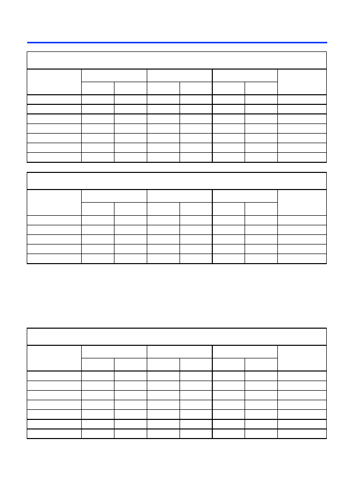
72
Altera Corporation
FLEX 10KE Embedded Programmable Logic Devices Data Sheet
Notes to tables:
(1)
All timing parameters are described in
Tables 24
through
30
in this data sheet.
(2)
These parameters are specified by characterization.
Tables 45
through
51
show EPF10K100E device internal and external
timing parameters.
Table 43. EPF10K50E External Timing Parameters
Notes (1)
,
(2)
Symbol
-1 Speed Grade
-2 Speed Grade
-3 Speed Grade
Unit
Min
Max
Min
Max
Min
Max
t
DRR
8.5
10.0
13.5
ns
t
INSU
2.7
3.2
4.3
ns
t
INH
0.0
0.0
0.0
ns
t
OUTCO
2.0
4.5
2.0
5.2
2.0
7.3
ns
t
PCISU
3.0
4.2
-
ns
t
PCIH
0.0
0.0
-
ns
t
PCICO
2.0
6.0
2.0
7.7
-
-
ns
Table 44. EPF10K50E External Bidirectional Timing Parameters
Notes (1)
,
(2)
Symbol
-1 Speed Grade
-2 Speed Grade
-3 Speed Grade
Unit
Min
Max
Min
Max
Min
Max
t
INSUBIDIR
2.7
3.2
4.3
ns
t
INHBIDIR
0.0
0.0
0.0
ns
t
OUTCOBIDIR
2.0
4.5
2.0
5.2
2.0
7.3
ns
t
XZBIDIR
6.8
7.8
10.1
ns
t
ZXBIDIR
6.8
7.8
10.1
ns
Table 45. EPF10K100E Device LE Timing Microparameters
Note (1)
Symbol
-1 Speed Grade
-2 Speed Grade
-3 Speed Grade
Unit
Min
Max
Min
Max
Min
Max
t
LUT
0.7
1.0
1.5
ns
t
CLUT
0.5
0.7
0.9
ns
t
RLUT
0.6
0.8
1.1
ns
t
PACKED
0.3
0.4
0.5
ns
t
EN
0.2
0.3
0.3
ns
t
CICO
0.1
0.1
0.2
ns
t
CGEN
0.4
0.5
0.7
ns

Altera Corporation
73
FLEX 10KE Embedded Programmable Logic Devices Data Sheet
t
CGENR
0.1
0.1
0.2
ns
t
CASC
0.6
0.9
1.2
ns
t
C
0.8
1.0
1.4
ns
t
CO
0.6
0.8
1.1
ns
t
COMB
0.4
0.5
0.7
ns
t
SU
0.4
0.6
0.7
ns
t
H
0.5
0.7
0.9
ns
t
PRE
0.8
1.0
1.4
ns
t
CLR
0.8
1.0
1.4
ns
t
CH
1.5
2.0
2.5
ns
t
CL
1.5
2.0
2.5
ns
Table 46. EPF10K100E Device IOE Timing Microparameters
Note (1)
Symbol
-1 Speed Grade
-2 Speed Grade
-3 Speed Grade
Unit
Min
Max
Min
Max
Min
Max
t
IOD
1.7
2.0
2.6
ns
t
IOC
0.0
0.0
0.0
ns
t
IOCO
1.4
1.6
2.1
ns
t
IOCOMB
0.5
0.7
0.9
ns
t
IOSU
0.8
1.0
1.3
ns
t
IOH
0.7
0.9
1.2
ns
t
IOCLR
0.5
0.7
0.9
ns
t
OD1
3.0
4.2
5.6
ns
t
OD2
3.0
4.2
5.6
ns
t
OD3
4.0
5.5
7.3
ns
t
XZ
3.5
4.6
6.1
ns
t
ZX1
3.5
4.6
6.1
ns
t
ZX2
3.5
4.6
6.1
ns
t
ZX3
4.5
5.9
7.8
ns
t
INREG
2.0
2.6
3.5
ns
t
IOFD
0.5
0.8
1.2
ns
t
INCOMB
0.5
0.8
1.2
ns
Table 45. EPF10K100E Device LE Timing Microparameters
Note (1)
Symbol
-1 Speed Grade
-2 Speed Grade
-3 Speed Grade
Unit
Min
Max
Min
Max
Min
Max
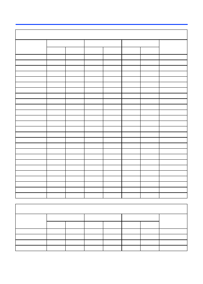
74
Altera Corporation
FLEX 10KE Embedded Programmable Logic Devices Data Sheet
Table 47. EPF10K100E Device EAB Internal Microparameters
Note (1)
Symbol
-1 Speed Grade
-2 Speed Grade
-3 Speed Grade
Unit
Min
Max
Min
Max
Min
Max
t
EABDATA1
1.5
2.0
2.6
ns
t
EABDATA1
0.0
0.0
0.0
ns
t
EABWE1
1.5
2.0
2.6
ns
t
EABWE2
0.3
0.4
0.5
ns
t
EABRE1
0.3
0.4
0.5
ns
t
EABRE2
0.0
0.0
0.0
ns
t
EABCLK
0.0
0.0
0.0
ns
t
EABCO
0.3
0.4
0.5
ns
t
EABBYPASS
0.1
0.1
0.2
ns
t
EABSU
0.8
1.0
1.4
ns
t
EABH
0.1
0.1
0.2
ns
t
EABCLR
0.3
0.4
0.5
ns
t
AA
4.0
5.1
6.6
ns
t
WP
2.7
3.5
4.7
ns
t
RP
1.0
1.3
1.7
ns
t
WDSU
1.0
1.3
1.7
ns
t
WDH
0.2
0.2
0.3
ns
t
WASU
1.6
2.1
2.8
ns
t
WAH
1.6
2.1
2.8
ns
t
RASU
3.0
3.9
5.2
ns
t
RAH
0.1
0.1
0.2
ns
t
WO
1.5
2.0
2.6
ns
t
DD
1.5
2.0
2.6
ns
t
EABOUT
0.2
0.3
0.3
ns
t
EABCH
1.5
2.0
2.5
ns
t
EABCL
2.7
3.5
4.7
ns
Table 48. EPF10K100E Device EAB Internal Timing Macroparameters (Part 1 of 2)
Note (1)
Symbol
-1 Speed Grade
-2 Speed Grade
-3 Speed Grade
Unit
Min
Max
Min
Max
Min
Max
t
EABAA
5.9
7.6
9.9
ns
t
EABRCOMB
5.9
7.6
9.9
ns
t
EABRCREG
5.1
6.5
8.5
ns
t
EABWP
2.7
3.5
4.7
ns

Altera Corporation
75
FLEX 10KE Embedded Programmable Logic Devices Data Sheet
t
EABWCOMB
5.9
7.7
10.3
ns
t
EABWCREG
5.4
7.0
9.4
ns
t
EABDD
3.4
4.5
5.9
ns
t
EABDATACO
0.5
0.7
0.8
ns
t
EABDATASU
0.8
1.0
1.4
ns
t
EABDATAH
0.1
0.1
0.2
ns
t
EABWESU
1.1
1.4
1.9
ns
t
EABWEH
0.0
0.0
0.0
ns
t
EABWDSU
1.0
1.3
1.7
ns
t
EABWDH
0.2
0.2
0.3
ns
t
EABWASU
4.1
5.2
6.8
ns
t
EABWAH
0.0
0.0
0.0
ns
t
EABWO
3.4
4.5
5.9
ns
Table 49. EPF10K100E Device Interconnect Timing Microparameters
Note (1)
Symbol
-1 Speed Grade
-2 Speed Grade
-3 Speed Grade
Unit
Min
Max
Min
Max
Min
Max
t
DIN2IOE
3.1
3.6
4.4
ns
t
DIN2LE
0.3
0.4
0.5
ns
t
DIN2DATA
1.6
1.8
2.0
ns
t
DCLK2IOE
0.8
1.1
1.4
ns
t
DCLK2LE
0.3
0.4
0.5
ns
t
SAMELAB
0.1
0.1
0.2
ns
t
SAMEROW
1.5
2.5
3.4
ns
t
SAMECOLUMN
0.4
1.0
1.6
ns
t
DIFFROW
1.9
3.5
5.0
ns
t
TWOROWS
3.4
6.0
8.4
ns
t
LEPERIPH
4.3
5.4
6.5
ns
t
LABCARRY
0.5
0.7
0.9
ns
t
LABCASC
0.8
1.0
1.4
ns
Table 48. EPF10K100E Device EAB Internal Timing Macroparameters (Part 2 of 2)
Note (1)
Symbol
-1 Speed Grade
-2 Speed Grade
-3 Speed Grade
Unit
Min
Max
Min
Max
Min
Max
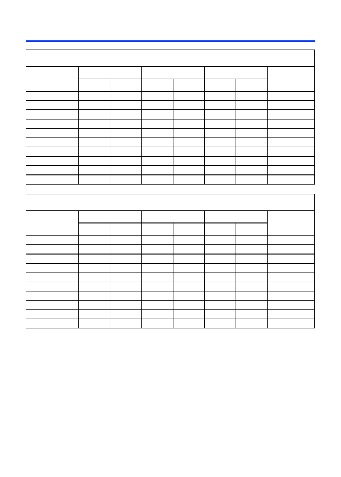
76
Altera Corporation
FLEX 10KE Embedded Programmable Logic Devices Data Sheet
Notes to tables:
(1)
All timing parameters are described in
Tables 24
through
30
in this data sheet.
(2)
These parameters are specified by characterization.
(3)
This parameter is measured without the use of the ClockLock or ClockBoost circuits.
(4)
This parameter is measured with the use of the ClockLock or ClockBoost circuits.
Table 50. EPF10K100E External Timing Parameters
Notes (1)
,
(2)
Symbol
-1 Speed Grade
-2 Speed Grade
-3 Speed Grade
Unit
Min
Max
Min
Max
Min
Max
t
DRR
9.0
12.0
16.0
ns
t
INSU
(3)
2.0
2.5
3.3
ns
t
INH
(3)
0.0
0.0
0.0
ns
t
OUTCO
(3)
2.0
5.2
2.0
6.9
2.0
9.1
ns
t
INSU
(4)
2.0
2.2
≠
ns
t
INH
(4)
0.0
0.0
≠
ns
t
OUTCO
(4)
0.5
3.0
0.5
4.6
≠
≠
ns
t
PCISU
3.0
6.2
≠
ns
t
PCIH
0.0
0.0
≠
ns
t
PCICO
2.0
6.0
2.0
6.9
≠
≠
ns
Table 51. EPF10K100E External Bidirectional Timing Parameters
Notes (1)
,
(2)
Symbol
-1 Speed Grade
-2 Speed Grade
-3 Speed Grade
Unit
Min
Max
Min
Max
Min
Max
t
INSUBIDIR
(3)
1.7
2.5
3.3
ns
t
INHBIDIR
(3)
0.0
0.0
0.0
ns
t
INSUBIDIR
(4)
2.0
2.8
≠
ns
t
INHBIDIR
(4)
0.0
0.0
≠
ns
t
OUTCOBIDIR
(3)
2.0
5.2
2.0
6.9
2.0
9.1
ns
t
XZBIDIR
(3)
5.6
7.5
10.1
ns
t
ZXBIDIR
(3)
5.6
7.5
10.1
ns
t
OUTCOBIDIR
(4)
0.5
3.0
0.5
4.6
≠
≠
ns
t
XZBIDIR
(4)
4.6
6.5
≠
ns
t
ZXBIDIR
(4)
4.6
6.5
≠
ns

Altera Corporation
77
FLEX 10KE Embedded Programmable Logic Devices Data Sheet
Tables 52
through
58
show EPF10K130E device internal and external
timing parameters.
Table 52. EPF10K130E Device LE Timing Microparameters
Note (1)
Symbol
-1 Speed Grade
-2 Speed Grade
-3 Speed Grade
Unit
Min
Max
Min
Max
Min
Max
t
LUT
0.6
0.9
1.3
ns
t
CLUT
0.6
0.8
1.0
ns
t
RLUT
0.7
0.9
0.2
ns
t
PACKED
0.3
0.5
0.6
ns
t
EN
0.2
0.3
0.4
ns
t
CICO
0.1
0.1
0.2
ns
t
CGEN
0.4
0.6
0.8
ns
t
CGENR
0.1
0.1
0.2
ns
t
CASC
0.6
0.9
1.2
ns
t
C
0.3
0.5
0.6
ns
t
CO
0.5
0.7
0.8
ns
t
COMB
0.3
0.5
0.6
ns
t
SU
0.5
0.7
0.8
ns
t
H
0.6
0.7
1.0
ns
t
PRE
0.9
1.2
1.6
ns
t
CLR
0.9
1.2
1.6
ns
t
CH
1.5
1.5
2.5
ns
t
CL
1.5
1.5
2.5
ns
Table 53. EPF10K130E Device IOE Timing Microparameters
Note (1)
Symbol
-1 Speed Grade
-2 Speed Grade
-3 Speed Grade
Unit
Min
Max
Min
Max
Min
Max
t
IOD
1.3
1.5
2.0
ns
t
IOC
0.0
0.0
0.0
ns
t
IOCO
0.6
0.8
1.0
ns
t
IOCOMB
0.6
0.8
1.0
ns
t
IOSU
1.0
1.2
1.6
ns
t
IOH
0.9
0.9
1.4
ns
t
IOCLR
0.6
0.8
1.0
ns
t
OD1
2.8
4.1
5.5
ns
t
OD2
2.8
4.1
5.5
ns

78
Altera Corporation
FLEX 10KE Embedded Programmable Logic Devices Data Sheet
t
OD3
4.0
5.6
7.5
ns
t
XZ
2.8
4.1
5.5
ns
t
ZX1
2.8
4.1
5.5
ns
t
ZX2
2.8
4.1
5.5
ns
t
ZX3
4.0
5.6
7.5
ns
t
INREG
2.5
3.0
4.1
ns
t
IOFD
0.4
0.5
0.6
ns
t
INCOMB
0.4
0.5
0.6
ns
Table 54. EPF10K130E Device EAB Internal Microparameters (Part 1 of 2)
Note (1)
Symbol
-1 Speed Grade
-2 Speed Grade
-3 Speed Grade
Unit
Min
Max
Min
Max
Min
Max
t
EABDATA1
1.5
2.0
2.6
ns
t
EABDATA2
0.0
0.0
0.0
ns
t
EABWE1
1.5
2.0
2.6
ns
t
EABWE2
0.3
0.4
0.5
ns
t
EABRE1
0.3
0.4
0.5
ns
t
EABRE2
0.0
0.0
0.0
ns
t
EABCLK
0.0
0.0
0.0
ns
t
EABCO
0.3
0.4
0.5
ns
t
EABBYPASS
0.1
0.1
0.2
ns
t
EABSU
0.8
1.0
1.4
ns
t
EABH
0.1
0.2
0.2
ns
t
EABCLR
0.3
0.4
0.5
ns
t
AA
4.0
5.0
6.6
ns
t
WP
2.7
3.5
4.7
ns
t
RP
1.0
1.3
1.7
ns
t
WDSU
1.0
1.3
1.7
ns
t
WDH
0.2
0.2
0.3
ns
t
WASU
1.6
2.1
2.8
ns
t
WAH
1.6
2.1
2.8
ns
t
RASU
3.0
3.9
5.2
ns
t
RAH
0.1
0.1
0.2
ns
t
WO
1.5
2.0
2.6
ns
Table 53. EPF10K130E Device IOE Timing Microparameters
Note (1)
Symbol
-1 Speed Grade
-2 Speed Grade
-3 Speed Grade
Unit
Min
Max
Min
Max
Min
Max

Altera Corporation
79
FLEX 10KE Embedded Programmable Logic Devices Data Sheet
t
DD
1.5
2.0
2.6
ns
t
EABOUT
0.2
0.3
0.3
ns
t
EABCH
1.5
2.0
2.5
ns
t
EABCL
2.7
3.5
4.7
ns
Table 55. EPF10K130E Device EAB Internal Timing Macroparameters
Note (1)
Symbol
-1 Speed Grade
-2 Speed Grade
-3 Speed Grade
Unit
Min
Max
Min
Max
Min
Max
t
EABAA
5.9
7.5
9.9
ns
t
EABRCOMB
5.9
7.5
9.9
ns
t
EABRCREG
5.1
6.4
8.5
ns
t
EABWP
2.7
3.5
4.7
ns
t
EABWCOMB
5.9
7.7
10.3
ns
t
EABWCREG
5.4
7.0
9.4
ns
t
EABDD
3.4
4.5
5.9
ns
t
EABDATACO
0.5
0.7
0.8
ns
t
EABDATASU
0.8
1.0
1.4
ns
t
EABDATAH
0.1
0.1
0.2
ns
t
EABWESU
1.1
1.4
1.9
ns
t
EABWEH
0.0
0.0
0.0
ns
t
EABWDSU
1.0
1.3
1.7
ns
t
EABWDH
0.2
0.2
0.3
ns
t
EABWASU
4.1
5.1
6.8
ns
t
EABWAH
0.0
0.0
0.0
ns
t
EABWO
3.4
4.5
5.9
ns
Table 54. EPF10K130E Device EAB Internal Microparameters (Part 2 of 2)
Note (1)
Symbol
-1 Speed Grade
-2 Speed Grade
-3 Speed Grade
Unit
Min
Max
Min
Max
Min
Max

80
Altera Corporation
FLEX 10KE Embedded Programmable Logic Devices Data Sheet
Table 56. EPF10K130E Device Interconnect Timing Microparameters
Note (1)
Symbol
-1 Speed Grade
-2 Speed Grade
-3 Speed Grade
Unit
Min
Max
Min
Max
Min
Max
t
DIN2IOE
2.8
3.5
4.4
ns
t
DIN2LE
0.7
1.2
1.6
ns
t
DIN2DATA
1.6
1.9
2.2
ns
t
DCLK2IOE
1.6
2.1
2.7
ns
t
DCLK2LE
0.7
1.2
1.6
ns
t
SAMELAB
0.1
0.2
0.2
ns
t
SAMEROW
1.9
3.4
5.1
ns
t
SAMECOLUMN
0.9
2.6
4.4
ns
t
DIFFROW
2.8
6.0
9.5
ns
t
TWOROWS
4.7
9.4
14.6
ns
t
LEPERIPH
3.1
4.7
6.9
ns
t
LABCARRY
0.6
0.8
1.0
ns
t
LABCASC
0.9
1.2
1.6
ns
Table 57. EPF10K130E External Timing Parameters
Notes (1)
,
(2)
Symbol
-1 Speed Grade
-2 Speed Grade
-3 Speed Grade
Unit
Min
Max
Min
Max
Min
Max
t
DRR
9.0
12.0
16.0
ns
t
INSU
(3)
1.9
2.1
3.0
ns
t
INH
(3)
0.0
0.0
0.0
ns
t
OUTCO
(3)
2.0
5.0
2.0
7.0
2.0
9.2
ns
t
INSU
(4)
0.9
1.1
≠
ns
t
INH
(4)
0.0
0.0
≠
ns
t
OUTCO
(4)
0.5
4.0
0.5
6.0
≠
≠
ns
t
PCISU
3.0
6.2
≠
ns
t
PCIH
0.0
0.0
≠
ns
t
PCICO
2.0
6.0
2.0
6.9
≠
≠
ns

Altera Corporation
81
FLEX 10KE Embedded Programmable Logic Devices Data Sheet
Notes to tables:
(1)
All timing parameters are described in
Tables 24
through
30
in this data sheet.
(2)
These parameters are specified by characterization.
(3)
This parameter is measured without the use of the ClockLock or ClockBoost circuits.
(4)
This parameter is measured with the use of the ClockLock or ClockBoost circuits.
Tables 59
through
65
show EPF10K200E device internal and external
timing parameters.
Table 58. EPF10K130E External Bidirectional Timing Parameters
Notes (1)
,
(2)
Symbol
-1 Speed Grade
-2 Speed Grade
-3 Speed Grade
Unit
Min
Max
Min
Max
Min
Max
t
INSUBIDIR
(3)
2.2
2.4
3.2
ns
t
INHBIDIR
(3)
0.0
0.0
0.0
ns
t
INSUBIDIR
(4)
2.8
3.0
≠
ns
t
INHBIDIR
(4)
0.0
0.0
≠
ns
t
OUTCOBIDIR
(3)
2.0
5.0
2.0
7.0
2.0
9.2
ns
t
XZBIDIR
(3)
5.6
8.1
10.8
ns
t
ZXBIDIR
(3)
5.6
8.1
10.8
ns
t
OUTCOBIDIR
(4)
0.5
4.0
0.5
6.0
≠
≠
ns
t
XZBIDIR
(4)
4.6
7.1
≠
ns
t
ZXBIDIR
(4)
4.6
7.1
≠
ns
Table 59. EPF10K200E Device LE Timing Microparameters (Part 1 of 2)
Note (1)
Symbol
-1 Speed Grade
-2 Speed Grade
-3 Speed Grade
Unit
Min
Max
Min
Max
Min
Max
t
LUT
0.7
0.8
1.2
ns
t
CLUT
0.4
0.5
0.6
ns
t
RLUT
0.6
0.7
0.9
ns
t
PACKED
0.3
0.5
0.7
ns
t
EN
0.4
0.5
0.6
ns
t
CICO
0.2
0.2
0.3
ns
t
CGEN
0.4
0.4
0.6
ns
t
CGENR
0.2
0.2
0.3
ns
t
CASC
0.7
0.8
1.2
ns
t
C
0.5
0.6
0.8
ns
t
CO
0.5
0.6
0.8
ns
t
COMB
0.4
0.6
0.8
ns
t
SU
0.4
0.6
0.7
ns
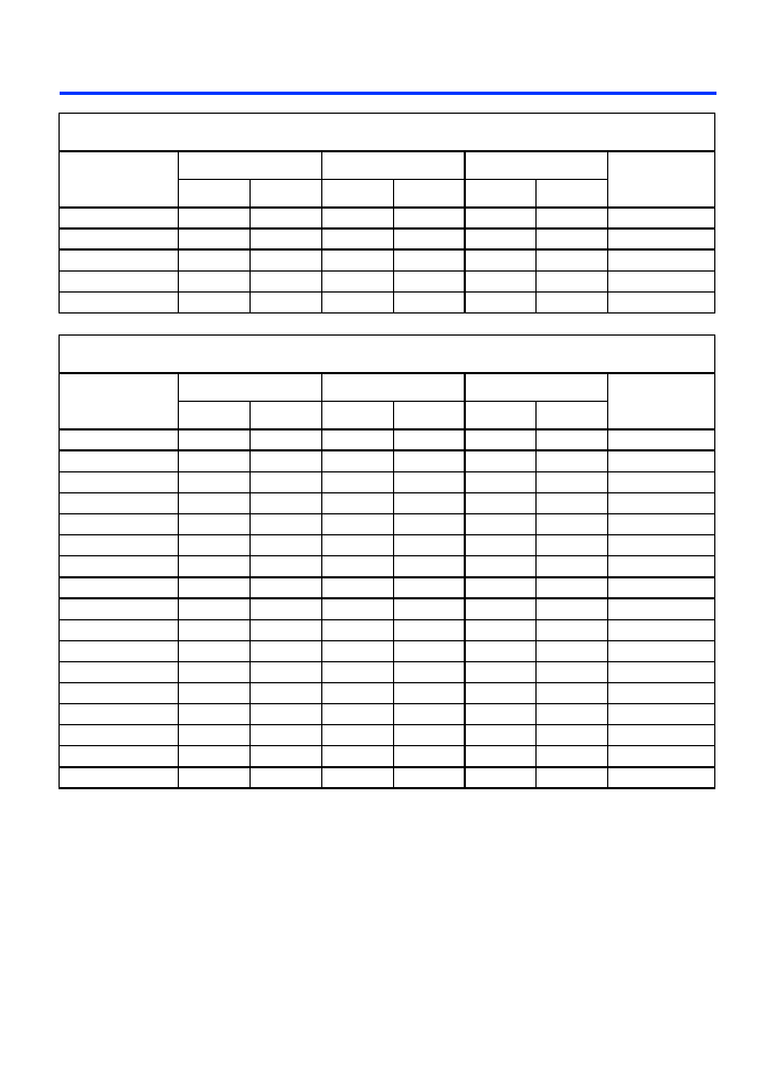
82
Altera Corporation
FLEX 10KE Embedded Programmable Logic Devices Data Sheet
t
H
0.9
1.1
1.5
ns
t
PRE
0.5
0.6
0.8
ns
t
CLR
0.5
0.6
0.8
ns
t
CH
2.0
2.5
3.0
ns
t
CL
2.0
2.5
3.0
ns
Table 60. EPF10K200E Device IOE Timing Microparameters
Note (1)
Symbol
-1 Speed Grade
-2 Speed Grade
-3 Speed Grade
Unit
Min
Max
Min
Max
Min
Max
t
IOD
1.6
1.9
2.6
ns
t
IOC
0.3
0.3
0.5
ns
t
IOCO
1.6
1.9
2.6
ns
t
IOCOMB
0.5
0.6
0.8
ns
t
IOSU
0.8
0.9
1.2
ns
t
IOH
0.7
0.8
1.1
ns
t
IOCLR
0.2
0.2
0.3
ns
t
OD1
0.6
0.7
0.9
ns
t
OD2
0.1
0.2
0.7
ns
t
OD3
2.5
3.0
3.9
ns
t
XZ
4.4
5.3
7.1
ns
t
ZX1
4.4
5.3
7.1
ns
t
ZX2
3.9
4.8
6.9
ns
t
ZX3
6.3
7.6
10.1
ns
t
INREG
4.8
5.7
7.7
ns
t
IOFD
1.5
1.8
2.4
ns
t
INCOMB
1.5
1.8
2.4
ns
Table 59. EPF10K200E Device LE Timing Microparameters (Part 2 of 2)
Note (1)
Symbol
-1 Speed Grade
-2 Speed Grade
-3 Speed Grade
Unit
Min
Max
Min
Max
Min
Max

Altera Corporation
83
FLEX 10KE Embedded Programmable Logic Devices Data Sheet
Table 61. EPF10K200E Device EAB Internal Microparameters
Note (1)
Symbol
-1 Speed Grade
-2 Speed Grade
-3 Speed Grade
Unit
Min
Max
Min
Max
Min
Max
t
EABDATA1
2.0
2.4
3.2
ns
t
EABDATA1
0.4
0.5
0.6
ns
t
EABWE1
1.4
1.7
2.3
ns
t
EABWE2
0.0
0.0
0.0
ns
t
EABRE1
0
0
0
ns
t
EABRE2
0.4
0.5
0.6
ns
t
EABCLK
0.0
0.0
0.0
ns
t
EABCO
0.8
0.9
1.2
ns
t
EABBYPASS
0.0
0.1
0.1
ns
t
EABSU
0.9
1.1
1.5
ns
t
EABH
0.4
0.5
0.6
ns
t
EABCLR
0.8
0.9
1.2
ns
t
AA
3.1
3.7
4.9
ns
t
WP
3.3
4.0
5.3
ns
t
RP
0.9
1.1
1.5
ns
t
WDSU
0.9
1.1
1.5
ns
t
WDH
0.1
0.1
0.1
ns
t
WASU
1.3
1.6
2.1
ns
t
WAH
2.1
2.5
3.3
ns
t
RASU
2.2
2.6
3.5
ns
t
RAH
0.1
0.1
0.2
ns
t
WO
2.0
2.4
3.2
ns
t
DD
2.0
2.4
3.2
ns
t
EABOUT
0.0
0.1
0.1
ns
t
EABCH
1.5
2.0
2.5
ns
t
EABCL
3.3
4.0
5.3
ns
Table 62. EPF10K200E Device EAB Internal Timing Macroparameters (Part 1 of 2)
Note (1)
Symbol
-1 Speed Grade
-2 Speed Grade
-3 Speed Grade
Unit
Min
Max
Min
Max
Min
Max
t
EABAA
5.1
6.4
8.4
ns
t
EABRCOMB
5.1
6.4
8.4
ns
t
EABRCREG
4.8
5.7
7.6
ns
t
EABWP
3.3
4.0
5.3
ns

84
Altera Corporation
FLEX 10KE Embedded Programmable Logic Devices Data Sheet
t
EABWCOMB
6.7
8.1
10.7
ns
t
EABWCREG
6.6
8.0
10.6
ns
t
EABDD
4.0
5.1
6.7
ns
t
EABDATACO
0.8
1.0
1.3
ns
t
EABDATASU
1.3
1.6
2.1
ns
t
EABDATAH
0.0
0.0
0.0
ns
t
EABWESU
0.9
1.1
1.5
ns
t
EABWEH
0.4
0.5
0.6
ns
t
EABWDSU
1.5
1.8
2.4
ns
t
EABWDH
0.0
0.0
0.0
ns
t
EABWASU
3.0
3.6
4.7
ns
t
EABWAH
0.4
0.5
0.7
ns
t
EABWO
3.4
4.4
5.8
ns
Table 63. EPF10K200E Device Interconnect Timing Microparameters
Note (1)
Symbol
-1 Speed Grade
-2 Speed Grade
-3 Speed Grade
Unit
Min
Max
Min
Max
Min
Max
t
DIN2IOE
4.2
4.6
5.7
ns
t
DIN2LE
1.7
1.7
2.0
ns
t
DIN2DATA
1.9
2.1
3.0
ns
t
DCLK2IOE
2.5
2.9
4.0
ns
t
DCLK2LE
1.7
1.7
2.0
ns
t
SAMELAB
0.1
0.1
0.2
ns
t
SAMEROW
2.3
2.6
3.6
ns
t
SAMECOLUMN
2.5
2.7
4.1
ns
t
DIFFROW
4.8
5.3
7.7
ns
t
TWOROWS
7.1
7.9
11.3
ns
t
LEPERIPH
7.0
7.6
9.0
ns
t
LABCARRY
0.1
0.1
0.2
ns
t
LABCASC
0.9
1.0
1.4
ns
Table 62. EPF10K200E Device EAB Internal Timing Macroparameters (Part 2 of 2)
Note (1)
Symbol
-1 Speed Grade
-2 Speed Grade
-3 Speed Grade
Unit
Min
Max
Min
Max
Min
Max
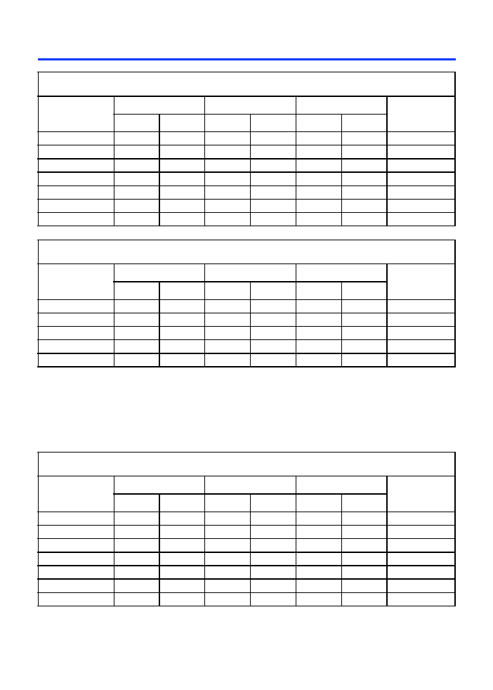
Altera Corporation
85
FLEX 10KE Embedded Programmable Logic Devices Data Sheet
Notes to tables:
(1)
All timing parameters are described in
Tables 24
through
30
in this data sheet.
(2)
These parameters are specified by characterization.
Tables 66
through
79
show EPF10K50S and EPF10K200S device external
timing parameters.
Table 64. EPF10K200E External Timing Parameters
Notes (1)
,
(2)
Symbol
-1 Speed Grade
-2 Speed Grade
-3 Speed Grade
Unit
Min
Max
Min
Max
Min
Max
t
DRR
10.0
12.0
16.0
ns
t
INSU
2.8
3.4
4.4
ns
t
INH
0.0
0.0
0.0
ns
t
OUTCO
2.0
4.5
2.0
5.3
2.0
7.8
ns
t
PCISU
3.0
6.2
-
ns
t
PCIH
0.0
0.0
-
ns
t
PCICO
2.0
6.0
2.0
8.9
-
-
ns
Table 65. EPF10K200E External Bidirectional Timing Parameters
Notes (1)
,
(2)
Symbol
-1 Speed Grade
-2 Speed Grade
-3 Speed Grade
Unit
Min
Max
Min
Max
Min
Max
t
INSUBIDIR
3.0
4.0
5.5
ns
t
INHBIDIR
0.0
0.0
0.0
ns
t
OUTCOBIDIR
2.0
4.5
2.0
5.3
2.0
7.8
ns
t
XZBIDIR
8.1
9.5
13.0
ns
t
ZXBIDIR
8.1
9.5
13.0
ns
Table 66. EPF10K50S Device LE Timing Microparameters (Part 1 of 2)
Note (1)
Symbol
-1 Speed Grade
-2 Speed Grade
-3 Speed Grade
Unit
Min
Max
Min
Max
Min
Max
t
LUT
0.6
0.8
1.1
ns
t
CLUT
0.5
0.6
0.8
ns
t
RLUT
0.6
0.7
0.9
ns
t
PACKED
0.2
0.3
0.4
ns
t
EN
0.6
0.7
0.9
ns
t
CICO
0.1
0.1
0.1
ns
t
CGEN
0.4
0.5
0.6
ns

86
Altera Corporation
FLEX 10KE Embedded Programmable Logic Devices Data Sheet
t
CGENR
0.1
0.1
0.1
ns
t
CASC
0.5
0.8
1.0
ns
t
C
0.5
0.6
0.8
ns
t
CO
0.6
0.6
0.7
ns
t
COMB
0.3
0.4
0.5
ns
t
SU
0.5
0.6
0.7
ns
t
H
0.5
0.6
0.8
ns
t
PRE
0.4
0.5
0.7
ns
t
CLR
0.8
1.0
1.2
ns
t
CH
2.0
2.5
3.0
ns
t
CL
2.0
2.5
3.0
ns
Table 67. EPF10K50S Device IOE Timing Microparameters
Note (1)
Symbol
-1 Speed Grade
-2 Speed Grade
-3 Speed Grade
Unit
Min
Max
Min
Max
Min
Max
t
IOD
1.3
1.3
1.9
ns
t
IOC
0.3
0.4
0.4
ns
t
IOCO
1.7
2.1
2.6
ns
t
IOCOMB
0.5
0.6
0.8
ns
t
IOSU
0.8
1.0
1.3
ns
t
IOH
0.4
0.5
0.6
ns
t
IOCLR
0.2
0.2
0.4
ns
t
OD1
1.2
1.2
1.9
ns
t
OD2
0.7
0.8
1.7
ns
t
OD3
2.7
3.0
4.3
ns
t
XZ
4.7
5.7
7.5
ns
t
ZX1
4.7
5.7
7.5
ns
t
ZX2
4.2
5.3
7.3
ns
t
ZX3
6.2
7.5
9.9
ns
t
INREG
3.5
4.2
5.6
ns
t
IOFD
1.1
1.3
1.8
ns
t
INCOMB
1.1
1.3
1.8
ns
Table 66. EPF10K50S Device LE Timing Microparameters (Part 2 of 2)
Note (1)
Symbol
-1 Speed Grade
-2 Speed Grade
-3 Speed Grade
Unit
Min
Max
Min
Max
Min
Max

Altera Corporation
87
FLEX 10KE Embedded Programmable Logic Devices Data Sheet
Table 68. EPF10K50S Device EAB Internal Microparameters
Note (1)
Symbol
-1 Speed Grade
-2 Speed Grade
-3 Speed Grade
Unit
Min
Max
Min
Max
Min
Max
t
EABDATA1
1.7
2.4
3.2
ns
t
EABDATA2
0.4
0.6
0.8
ns
t
EABWE1
1.0
1.4
1.9
ns
t
EABWE2
0.0
0.0
0.0
ns
t
EABRE1
0.0
0.0
0.0
t
EABRE2
0.4
0.6
0.8
t
EABCLK
0.0
0.0
0.0
ns
t
EABCO
0.8
1.1
1.5
ns
t
EABBYPASS
0.0
0.0
0.0
ns
t
EABSU
0.7
1.0
1.3
ns
t
EABH
0.4
0.6
0.8
ns
t
EABCLR
0.8
1.1
1.5
t
AA
2.0
2.8
3.8
ns
t
WP
2.0
2.8
3.8
ns
t
RP
1.0
1.4
1.9
t
WDSU
0.5
0.7
0.9
ns
t
WDH
0.1
0.1
0.2
ns
t
WASU
1.0
1.4
1.9
ns
t
WAH
1.5
2.1
2.9
ns
t
RASU
1.5
2.1
2.8
t
RAH
0.1
0.1
0.2
t
WO
2.1
2.9
4.0
ns
t
DD
2.1
2.9
4.0
ns
t
EABOUT
0.0
0.0
0.0
ns
t
EABCH
1.5
2.0
2.5
ns
t
EABCL
1.5
2.0
2.5
ns

88
Altera Corporation
FLEX 10KE Embedded Programmable Logic Devices Data Sheet
Table 69. EPF10K50S Device EAB Internal Timing Macroparameters
Note (1)
Symbol
-1 Speed Grade
-2 Speed Grade
-3 Speed Grade
Unit
Min
Max
Min
Max
Min
Max
t
EABAA
3.7
5.2
7.0
ns
t
EABRCCOMB
3.7
5.2
7.0
ns
t
EABRCREG
3.5
4.9
6.6
ns
t
EABWP
2.0
2.8
3.8
ns
t
EABWCCOMB
4.5
6.3
8.6
ns
t
EABWCREG
5.6
7.8
10.6
ns
t
EABDD
3.8
5.3
7.2
ns
t
EABDATACO
0.8
1.1
1.5
ns
t
EABDATASU
1.1
1.6
2.1
ns
t
EABDATAH
0.0
0.0
0.0
ns
t
EABWESU
0.7
1.0
1.3
ns
t
EABWEH
0.4
0.6
0.8
ns
t
EABWDSU
1.2
1.7
2.2
ns
t
EABWDH
0.0
0.0
0.0
ns
t
EABWASU
1.6
2.3
3.0
ns
t
EABWAH
0.9
1.2
1.8
ns
t
EABWO
3.1
4.3
5.9
ns
Table 70. EPF10K50S Device Interconnect Timing Microparameters
Note (1)
Symbol
-1 Speed Grade
-2 Speed Grade
-3 Speed Grade
Unit
Min
Max
Min
Max
Min
Max
t
DIN2IOE
3.1
3.7
4.6
ns
t
DIN2LE
1.7
2.1
2.7
ns
t
DIN2DATA
2.7
3.1
5.1
ns
t
DCLK2IOE
1.6
1.9
2.6
ns
t
DCLK2LE
1.7
2.1
2.7
ns
t
SAMELAB
0.1
0.1
0.2
ns
t
SAMEROW
1.5
1.7
2.4
ns
t
SAMECOLUMN
1.0
1.3
2.1
ns
t
DIFFROW
2.5
3.0
4.5
ns
t
TWOROWS
4.0
4.7
6.9
ns
t
LEPERIPH
2.6
2.9
3.4
ns
t
LABCARRY
0.1
0.2
0.2
ns
t
LABCASC
0.8
1.0
1.3
ns

Altera Corporation
89
FLEX 10KE Embedded Programmable Logic Devices Data Sheet
Notes to tables:
(1)
All timing parameters are described in
Tables 24
through
30
.
(2)
This parameter is measured without use of the ClockLock or ClockBoost circuits.
(3)
This parameter is measured with use of the ClockLock or ClockBoost circuits
Table 71. EPF10K50S External Timing Parameters
Note (1)
Symbol
-1 Speed Grade
-2 Speed Grade
-3 Speed Grade
Unit
Min
Max
Min
Max
Min
Max
t
DRR
8.0
9.5
12.5
ns
t
INSU
(2)
2.4
2.9
3.9
ns
t
INH
(2)
0.0
0.0
0.0
ns
t
OUTCO
(2)
2.0
4.3
2.0
5.2
2.0
7.3
ns
t
INSU
(3)
2.4
2.9
ns
t
INH
(3)
0.0
0.0
ns
t
OUTCO
(3)
0.5
3.3
0.5
4.1
ns
t
PCISU
2.4
2.9
≠
ns
t
PCIH
0.0
0.0
≠
ns
t
PCICO
2.0
6.0
2.0
7.7
≠
≠
ns
Table 72. EPF10K50S External Bidirectional Timing Parameters
Note (1)
Symbol
-1 Speed Grade
-2 Speed Grade
-3 Speed Grade
Unit
Min
Max
Min
Max
Min
Max
t
INSUBIDIR
(2)
2.7
3.2
4.3
ns
t
INHBIDIR
(2)
0.0
0.0
0.0
ns
t
INHBIDIR
(3)
0.0
0.0
≠
ns
t
INSUBIDIR
(3)
3.7
4.2
≠
ns
t
OUTCOBIDIR
(2)
2.0
4.5
2.0
5.2
2.0
7.3
ns
t
XZBIDIR
(2)
6.8
7.8
10.1
ns
t
ZXBIDIR
(2)
6.8
7.8
10.1
ns
t
OUTCOBIDIR
(3)
0.5
3.5
0.5
4.2
≠
≠
t
XZBIDIR
(3)
6.8
8.4
≠
ns
t
ZXBIDIR
(3)
6.8
8.4
≠
ns

90
Altera Corporation
FLEX 10KE Embedded Programmable Logic Devices Data Sheet
Table 73. EPF10K200S Device Internal & External Timing Parameters
Note (1)
Symbol
-1 Speed Grade
-2 Speed Grade
-3 Speed Grade
Unit
Min
Max
Min
Max
Min
Max
t
LUT
0.7
0.8
1.2
ns
t
CLUT
0.4
0.5
0.6
ns
t
RLUT
0.5
0.7
0.9
ns
t
PACKED
0.4
0.5
0.7
ns
t
EN
0.6
0.5
0.6
ns
t
CICO
0.1
0.2
0.3
ns
t
CGEN
0.3
0.4
0.6
ns
t
CGENR
0.1
0.2
0.3
ns
t
CASC
0.7
0.8
1.2
ns
t
C
0.5
0.6
0.8
ns
t
CO
0.5
0.6
0.8
ns
t
COMB
0.3
0.6
0.8
ns
t
SU
0.4
0.6
0.7
ns
t
H
1.0
1.1
1.5
ns
t
PRE
0.4
0.6
0.8
ns
t
CLR
0.5
0.6
0.8
ns
t
CH
2.0
2.5
3.0
ns
t
CL
2.0
2.5
3.0
ns
Table 74. EPF10K200S Device IOE Timing Microparameters (Part 1 of 2)
Note (1)
Symbol
-1 Speed Grade
-2 Speed Grade
-3 Speed Grade
Unit
Min
Max
Min
Max
Min
Max
t
IOD
1.8
1.9
2.6
ns
t
IOC
0.3
0.3
0.5
ns
t
IOCO
1.7
1.9
2.6
ns
t
IOCOMB
0.5
0.6
0.8
ns
t
IOSU
0.8
0.9
1.2
ns
t
IOH
0.4
0.8
1.1
ns
t
IOCLR
0.2
0.2
0.3
ns
t
OD1
1.3
0.7
0.9
ns
t
OD2
0.8
0.2
0.4
ns
t
OD3
2.9
3.0
3.9
ns
t
XZ
5.0
5.3
7.1
ns
t
ZX1
5.0
5.3
7.1
ns

Altera Corporation
91
FLEX 10KE Embedded Programmable Logic Devices Data Sheet
t
ZX2
4.5
4.8
6.6
ns
t
ZX3
6.6
7.6
10.1
ns
t
INREG
3.7
5.7
7.7
ns
t
IOFD
1.8
3.4
4.0
ns
t
INCOMB
1.8
3.4
4.0
ns
Table 75. EPF10K200S Device EAB Internal Microparameters
Note (1)
Symbol
-1 Speed Grade
-2 Speed Grade
-3 Speed Grade
Unit
Min
Max
Min
Max
Min
Max
t
EABDATA1
1.8
2.4
3.2
ns
t
EABDATA1
0.4
0.5
0.6
ns
t
EABWE1
1.1
1.7
2.3
ns
t
EABWE2
0.0
0.0
0.0
ns
t
EABRE1
0
0
0
ns
t
EABRE2
0.4
0.5
0.6
ns
t
EABCLK
0.0
0.0
0.0
ns
t
EABCO
0.8
0.9
1.2
ns
t
EABBYPASS
0.0
0.1
0.1
ns
t
EABSU
0.7
1.1
1.5
ns
t
EABH
0.4
0.5
0.6
ns
t
EABCLR
0.8
0.9
1.2
ns
t
AA
2.1
3.7
4.9
ns
t
WP
2.1
4.0
5.3
ns
t
RP
1.1
1.1
1.5
ns
t
WDSU
0.5
1.1
1.5
ns
t
WDH
0.1
0.1
0.1
ns
t
WASU
1.1
1.6
2.1
ns
t
WAH
1.6
2.5
3.3
ns
t
RASU
1.6
2.6
3.5
ns
t
RAH
0.1
0.1
0.2
ns
t
WO
2.0
2.4
3.2
ns
t
DD
2.0
2.4
3.2
ns
t
EABOUT
0.0
0.1
0.1
ns
t
EABCH
1.5
2.0
2.5
ns
t
EABCL
2.1
2.8
3.8
ns
Table 74. EPF10K200S Device IOE Timing Microparameters (Part 2 of 2)
Note (1)
Symbol
-1 Speed Grade
-2 Speed Grade
-3 Speed Grade
Unit
Min
Max
Min
Max
Min
Max
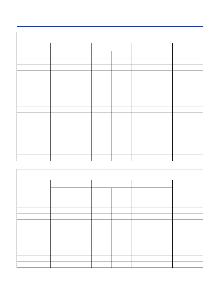
92
Altera Corporation
FLEX 10KE Embedded Programmable Logic Devices Data Sheet
Table 76. EPF10K200S Device EAB Internal Timing Macroparameters
Note (1)
Symbol
-1 Speed Grade
-2 Speed Grade
-3 Speed Grade
Unit
Min
Max
Min
Max
Min
Max
t
EABAA
3.9
6.4
8.4
ns
t
EABRCOMB
3.9
6.4
8.4
ns
t
EABRCREG
3.6
5.7
7.6
ns
t
EABWP
2.1
4.0
5.3
ns
t
EABWCOMB
4.8
8.1
10.7
ns
t
EABWCREG
5.4
8.0
10.6
ns
t
EABDD
3.8
5.1
6.7
ns
t
EABDATACO
0.8
1.0
1.3
ns
t
EABDATASU
1.1
1.6
2.1
ns
t
EABDATAH
0.0
0.0
0.0
ns
t
EABWESU
0.7
1.1
1.5
ns
t
EABWEH
0.4
0.5
0.6
ns
t
EABWDSU
1.2
1.8
2.4
ns
t
EABWDH
0.0
0.0
0.0
ns
t
EABWASU
1.9
3.6
4.7
ns
t
EABWAH
0.8
0.5
0.7
ns
t
EABWO
3.1
4.4
5.8
ns
Table 77. EPF10K200S Device Interconnect Timing Microparameters (Part 1 of 2)
Note (1)
Symbol
-1 Speed Grade
-2 Speed Grade
-3 Speed Grade
Unit
Min
Max
Min
Max
Min
Max
t
DIN2IOE
4.4
4.8
5.5
ns
t
DIN2LE
0.6
0.6
0.9
ns
t
DIN2DATA
1.8
2.1
2.8
ns
t
DCLK2IOE
1.7
2.0
2.8
ns
t
DCLK2LE
0.6
0.6
0.9
ns
t
SAMELAB
0.1
0.1
0.2
ns
t
SAMEROW
3.0
4.6
5.7
ns
t
SAMECOLUMN
3.5
4.9
6.4
ns
t
DIFFROW
6.5
9.5
12.1
ns
t
TWOROWS
9.5
14.1
17.8
ns
t
LEPERIPH
5.5
6.2
7.2
ns
t
LABCARRY
0.3
0.1
0.2
ns

Altera Corporation
93
FLEX 10KE Embedded Programmable Logic Devices Data Sheet
Notes to tables:
(1)
All timing parameters are described in
Tables 24
through
30
in this data sheet.
(2)
This parameter is measured without the use of the ClockLock or ClockBoost circuits.
(3)
This parameter is measured with the use of the ClockLock or ClockBoost circuits.
t
LABCASC
0.5
1.0
1.4
ns
Table 78. EPF10K200S External Timing Parameters
Note (1)
Symbol
-1 Speed Grade
-2 Speed Grade
-3 Speed Grade
Unit
Min
Max
Min
Max
Min
Max
t
DRR
9.0
12.0
16.0
ns
t
INSU
(2)
3.1
3.7
4.7
ns
t
INH
(2)
0.0
0.0
0.0
ns
t
OUTCO
(2)
2.0
3.7
2.0
4.4
2.0
6.3
ns
t
INSU
(3)
2.1
2.7
≠
ns
t
INH
(3)
0.0
0.0
≠
ns
t
OUTCO
(3)
0.5
2.7
0.5
3.4
≠
≠
ns
t
PCISU
3.0
4.2
≠
ns
t
PCIH
0.0
0.0
≠
ns
t
PCICO
2.0
6.0
2.0
8.9
≠
≠
ns
Table 79. EPF10K200S External Bidirectional Timing Parameters
Note (1)
Symbol
-1 Speed Grade
-2 Speed Grade
-3 Speed Grade
Unit
Min
Max
Min
Max
Min
Max
t
INSUBIDIR
(2)
2.3
3.4
4.4
ns
t
INHBIDIR
(2)
0.0
0.0
0.0
ns
t
INSUBIDIR
(3)
3.3
4.4
≠
ns
t
INHBIDIR
(3)
0.0
0.0
≠
ns
t
OUTCOBIDIR
(2)
2.0
3.7
2.0
4.4
2.0
6.3
ns
t
XZBIDIR
(2)
6.9
7.6
9.2
ns
t
ZXBIDIR
(2)
5.9
6.6
≠
ns
t
OUTCOBIDIR
(3)
0.5
2.7
0.5
3.4
≠
≠
ns
t
XZBIDIR
(3)
6.9
7.6
9.2
ns
t
ZXBIDIR
(3)
5.9
6.6
≠
ns
Table 77. EPF10K200S Device Interconnect Timing Microparameters (Part 2 of 2)
Note (1)
Symbol
-1 Speed Grade
-2 Speed Grade
-3 Speed Grade
Unit
Min
Max
Min
Max
Min
Max

94
Altera Corporation
FLEX 10KE Embedded Programmable Logic Devices Data Sheet
Power
Consumption
The supply power (P) for FLEX 10KE devices can be calculated with the
following equation:
P = P
INT
+ P
IO
= (I
CCSTANDBY
+ I
CCACTIVE)
◊
V
CC
+ P
IO
The I
CCACTIVE
value depends on the switching frequency and the
application logic. This value is calculated based on the amount of current
that each LE typically consumes. The P
IO
value, which depends on the
device output load characteristics and switching frequency, can be
calculated using the guidelines given in
Application Note 74 (Evaluating
Power for Altera Devices)
.
Compared to the rest of the device, the embedded array consumes a
negligible amount of power. Therefore, the embedded array can be
ignored when calculating supply current.
The I
CCACTIVE
value can be calculated with the following equation:
I
CCACTIVE
= K
◊
f
MAX
◊
N
◊
tog
LC
◊
Where:
f
MAX
=
Maximum operating frequency in MHz
N
=
Total number of LEs used in the device
tog
LC
=
Average percent of LEs toggling at each clock
(typically 12.5%)
K
=
Constant
Table 80
provides the constant (K) values for FLEX 10KE devices.
This calculation provides an I
CC
estimate based on typical conditions with
no output load. The actual I
CC
should be verified during operation
because this measurement is sensitive to the actual pattern in the device
and the environmental operating conditions.
Table 80. FLEX 10KE K Constant Values
Device
K Value
EPF10K30E
4.5
EPF10K50E
4.8
EPF10K50S
4.5
EPF10K100E
4.5
EPF10K130E
4.6
EPF10K200E
4.8
EPF10K200S
4.6
µ
A
MHz
LE
◊
---------------------------

Altera Corporation
95
FLEX 10KE Embedded Programmable Logic Devices Data Sheet
To better reflect actual designs, the power model (and the constant K in
the power calculation equations) for continuous interconnect FLEX
devices assumes that LEs drive FastTrack Interconnect channels. In
contrast, the power model of segmented FPGAs assumes that all LEs drive
only one short interconnect segment. This assumption may lead to
inaccurate results when compared to measured power consumption for
actual designs in segmented FPGAs.
Figure 31
shows the relationship between the current and operating
frequency of FLEX 10KE devices.
Figure 31. FLEX 10KE I
CCACTIVE
vs. Operating Frequency (Part 1 of 2)
0
Frequency (MHz)
I
CC
Supply
Current (mA)
100
80
60
40
20
50
100
EPF10K30E
0
Frequency (MHz)
I
CC
Supply
Current (mA)
200
150
100
50
50
100
EPF10K50S
0
Frequency (MHz)
300
200
100
50
100
EPF10K100E
I
CC
Supply
Current (mA)
0
Frequency (MHz)
I
CC
Supply
Current (mA)
200
150
100
50
50
100
EPF10K50E

96
Altera Corporation
FLEX 10KE Embedded Programmable Logic Devices Data Sheet
Figure
31
. FLEX 10KE I
CCACTIVE
vs. Operating Frequency (Part 2 of 2)
Configuration &
Operation
The FLEX 10KE architecture supports several configuration schemes. This
section summarizes the device operating modes and available device
configuration schemes.
Operating Modes
The FLEX 10KE architecture uses SRAM configuration elements that
require configuration data to be loaded every time the circuit powers up.
The process of physically loading the SRAM data into the device is called
configuration. Before configuration, as V
CC
rises, the device initiates a
Power-On Reset (POR). This POR event clears the device and prepares it
for configuration. The FLEX 10KE POR time does not exceed 50 µs.
When configuring with a configuration device, refer to the respective
configuration device data sheet for POR timing information.
0
Frequency (MHz)
600
400
200
50
100
EPF10K200S
I
CC
Supply
Current (mA)
0
Frequency (MHz)
400
300
200
100
50
100
EPF10K130E
I
CC
Supply
Current (mA)
0
Frequency (MHz)
600
400
200
50
100
EPF10K200E
I
CC
Supply
Current (mA)

Altera Corporation
97
FLEX 10KE Embedded Programmable Logic Devices Data Sheet
During initialization, which occurs immediately after configuration, the
device resets registers, enables I/O pins, and begins to operate as a logic
device. The I/O pins are tri-stated during power-up, and before and
during configuration. Together, the configuration and initialization
processes are called command mode; normal device operation is called user
mode.
SRAM configuration elements allow FLEX 10KE devices to be
reconfigured in-circuit by loading new configuration data into the device.
Real-time reconfiguration is performed by forcing the device into
command mode with a device pin, loading different configuration data,
reinitializing the device, and resuming user-mode operation. The entire
reconfiguration process requires less than 85 ms and can be used to
reconfigure an entire system dynamically. In-field upgrades can be
performed by distributing new configuration files.
Before and during configuration, all I/O pins (except dedicated inputs,
clock, or configuration pins) are pulled high by a weak pull-up resistor.
Programming Files
Despite being function- and pin-compatible, FLEX 10KE devices are not
programming- or configuration file-compatible with FLEX 10K or
FLEX 10KA devices. A design therefore must be recompiled before it is
transferred from a FLEX 10K or FLEX 10KA device to an equivalent
FLEX 10KE device. This recompilation should be performed both to create
a new programming or configuration file and to check design timing in
FLEX 10KE devices, which has different timing characteristics than
FLEX 10K or FLEX 10KA devices.
FLEX 10KE devices are generally pin-compatible with equivalent
FLEX 10KA devices. In some cases, FLEX 10KE devices have fewer I/O
pins than the equivalent FLEX 10KA devices.
Table 81
shows which
FLEX 10KE devices have fewer I/O pins than equivalent FLEX 10KA
devices. However, power, ground, JTAG, and configuration pins are the
same on FLEX 10KA and FLEX 10KE devices, enabling migration from a
FLEX 10KA design to a FLEX 10KE design.

98
Altera Corporation
FLEX 10KE Embedded Programmable Logic Devices Data Sheet
Additionally, the Altera software offers several features that help plan for
future device migration by preventing the use of conflicting I/O pins.
Configuration Schemes
The configuration data for a FLEX 10KE device can be loaded with one of
five configuration schemes (see
Table 82
), chosen on the basis of the target
application. An EPC1, EPC2, or EPC16 configuration device, intelligent
controller, or the JTAG port can be used to control the configuration of a
FLEX 10KE device, allowing automatic configuration on system
power-up.
Multiple FLEX 10KE devices can be configured in any of the five
configuration schemes by connecting the configuration enable (
nCE
) and
configuration enable output (
nCEO
) pins on each device. Additional
FLEX 10K, FLEX 10KA, FLEX 10KE, and FLEX 6000 devices can be
configured in the same serial chain.
Table 81. I/O Counts for FLEX 10KA & FLEX 10KE Devices
FLEX 10KA
FLEX 10KE
Device
I/O Count
Device
I/O Count
EPF10K30AF256
191
EPF10K30EF256
176
EPF10K30AF484
246
EPF10K30EF484
220
EPF10K50VB356
274
EPF10K50SB356
220
EPF10K50VF484
291
EPF10K50EF484
254
EPF10K50VF484
291
EPF10K50SF484
254
EPF10K100AF484
369
EPF10K100EF484
338
Table 82. Data Sources for FLEX 10KE Configuration
Configuration Scheme
Data Source
Configuration device
EPC1, EPC2, or EPC16 configuration device
Passive serial (PS)
BitBlaster, ByteBlasterMV, or MasterBlaster download cables,
or serial data source
Passive parallel asynchronous (PPA)
Parallel data source
Passive parallel synchronous (PPS)
Parallel data source
JTAG
BitBlaster or ByteBlasterMV download cables, or
microprocessor with a Jam STAPL file or JBC file

Altera Corporation
99
FLEX 10KE Embedded Programmable Logic Devices Data Sheet
Device
Pin-Outs
See the Altera web site (
http://www.altera.com
) or the Altera Digital
Library for pin-out information.
Revision
History
The information contained in the FLEX 10KE Embedded Programmable Logic
Data Sheet version 2.5 supersedes information published in previous
versions.
Version 2.5
The following changes were made to the FLEX 10KE Embedded
Programmable Logic Data Sheet version 2.5:
Note (1)
added to
Figure 23
.
Text added to
"I/O Element"
section on
page 34
.
Updated
Table 22
.
Version 2.4
The following changes were made to the FLEX 10KE Embedded
Programmable Logic Data Sheet version 2.4: updated text on
page 34
and
page 63
.

101 Innovation Drive
San Jose, CA 95134
(408) 544-7000
http://www.altera.com
Applications Hotline:
(800) 800-EPLD
Literature Services:
lit_req@altera.com
Copyright © 2003 Altera Corporation. All rights reserved. Altera, The Programmable Solutions Company, the
stylized Altera logo, specific device designations, and all other words and logos that are identified as
trademarks and/or service marks are, unless noted otherwise, the trademarks and service marks of Altera
Corporation in the U.S. and other countries. All other product or service names are the property of their
respective holders. Altera products are protected under numerous U.S. and foreign patents and pending
applications, maskwork rights, and copyrights. Altera warrants performance of its
semiconductor products to current specifications in accordance with Altera's standard
warranty, but reserves the right to make changes to any products and services at any time
without notice. Altera assumes no responsibility or liability arising out of the application
or use of any information, product, or service described herein except as expressly agreed
to in writing by Altera Corporation. Altera customers are advised to obtain the latest
version of device specifications before relying on any published information and before
placing orders for products or services
.
FLEX 10KE Embedded Programmable Logic Devices Data Sheet
100
Altera Corporation
Printed on Recycled Paper.