 | –≠–ª–µ–∫—Ç—Ä–æ–Ω–Ω—ã–π –∫–æ–º–ø–æ–Ω–µ–Ω—Ç: EV3019 | –°–∫–∞—á–∞—Ç—å:  PDF PDF  ZIP ZIP |

1
EV3019
SONET/SDH/ATM STS-12 TRANSCEIVER EVALUATION BOARD
September 22, 1999
EV3019
Æ
DESCRIPTION
The S3019 evaluation board provides a flexible platform for verifying the operation of the S3019 transceiver
interface circuit. This document provides information on the board contents. It should be used in conjunction with
the S3019 data sheet, which contains full technical details on the chips operation.
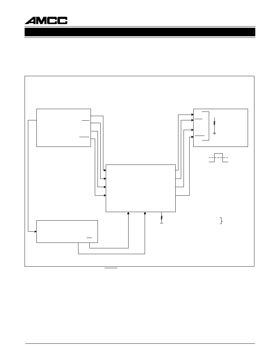
Figure 1 shows the outline of the S3019 evaluation board. Figure 2 shows the block diagram of how the S3019
evaluation board should be connected to test equipment for Bit Error Rate (BER) testing. Figure 3 shows the test
setup for BER measurements and jitter testing.
SONET/SDH/ATM STS-12 TRANSCEIVER EVALUATION BOARD
Figure 1. S3019 Evaluation Board Top View
GND
GND
GND
RSDP
RSDN
RSCLKP
RSCLKN
TSCLKP
TSCLKN
TSDN
TSDP
DUT
VEE
GND
DUT
VCC
REFCLKP
REFCLKN
TTLREF
GND
T51MCLK
T38MCLK
T19MCLK
PARERR
POCLK
PCLK
PICLK
PIN7
PIN6
PIN5
PIN4
PIN3
PIN2
PIN1
PIN0
GND
POUT7:0
PIN7:0
GND
OPEN
FOR NC
RXLOCKDET
PAROUT
FP
GND
RSTB
"1"
"0"
TSTRST
LLEB
RLPTIME
SQUELCH
SDTTL
SDPECL
DLEB
OOF
BYPASS
MODE1
MODE0
SLPTIME
PARIN
NC
"1"
"0"
6290 SEQUENCE DR.
SAN DIEGO, CA 92121
APPLIED MICRO CIRCUITS CORPORATION
S3019 SONET/SDH/ATM 0C-3/12 TRANSCEIVER WITH CDR
(MODE JUMPERS)
S3019
2
SONET/SDH/ATM STS-12 TRANSCEIVER EVALUATION BOARD
EV3019
September 22, 1999
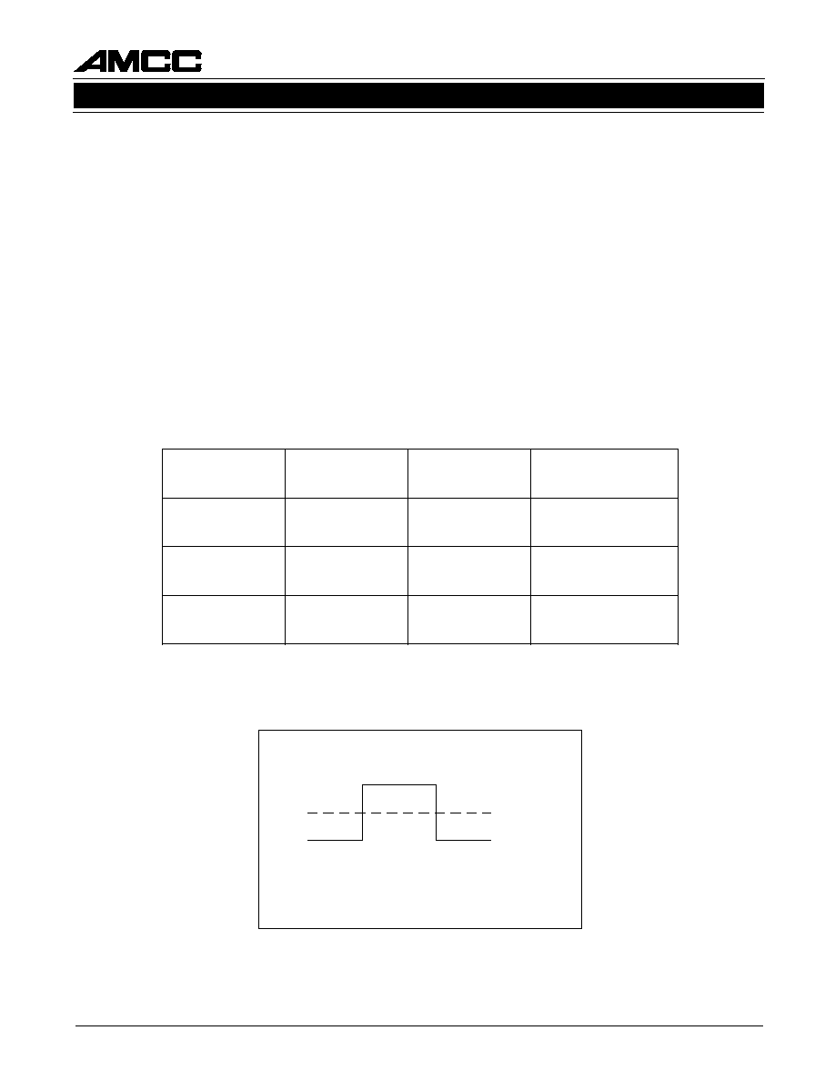
Figure 2 depicts how the S3019 evaluation board can be connected for BER measurements, and shows all of
the DIP switch settings. In addition, it shows the Level Shifted ECL (LSECL) power supply requirements for use
with test equipment that utilizes 50
to ground termination. In this configuration the S3019 is configured for use
with the internal S3019 Clock Recovery Unit (CRU), using a 19.44 MHz reference and operating at STS-12.
Figure 2. S3019 Bit Error Rate (BER) Test Setup
S3019 DUT
BERT TX (622MHz)
RSDP
RSDN
RSCLKP
RSCLKN
TSDP
TSDN
TSCLKP
TSCLKN
REFCLKP
REFCLKN
TTLREF
HP8133 PULSE
GENERATOR OR DIVIDER
BERT RX
DATA
CLOCK
DATA
CLOCK
DATA
CLOCK
DATA
CLOCK
CLOCK
EXT IN
OUT
(DIV BY 32)
OUT
S3019 BER
TEST
19.44MHz
+2V
POWER SUPPLY
DUT VCC = +2V
DUT VEE = -1.3V
±
5%
GND = 0V
DIP SWITCH SETTINGS:
TSTRST '0'
LLEB '1'
RLP TIME '0'
SQUELCH '0'
SDTTL '1'
SDPECL '0'
DLEB '1'
OOF '0'
MODE1 '0'
MODE0 '0'
BYPASS '0'
SLPTIME '0'
PARIN '0'
622MHz
LSECL CONFIGURATION
50
or not
connected
+1.2V
+0.2V
+0.7V
10k
FOR Example
19.44 MHz operation
Note: When using the internal CRU, CLOCK and CLOCK does not need to be connected to RSCLKP and RSCLKN.

3
EV3019
SONET/SDH/ATM STS-12 TRANSCEIVER EVALUATION BOARD
September 22, 1999
Figure 3 depicts how two S3019 evaluation boards can be connected for BER measurements and jitter testing,
and shows all of the DIP switch settings. In addition, it shows the power supply requirements for use with test
equipment that utilizes 50
to -2V termination. These settings are for STS-12 testing.
Figure 3. S3019 Evaluation Board BER Measurement and Jitter Testing Setup
DATA
CLOCK
DATA
DATA
CLOCK
TSCLKN
THRU DATA
REFCLK
DATA OUTPUT
RSDP
RSDN
PIN 0
PIN 1
PIN 2
PIN 3
PIN 4
PIN 5
PIN 6
PIN 7
PICLK
POUT 0
POUT 1
POUT 2
POUT 3
POUT 4
POUT 5
POUT 6
POUT7
POCLK
Trigger
MEASURE DATA EYE
Scope
FF00 (HEX) OR PRBS PATTERN
PROVIDES ASYNCRONOUS DATA
2
7
-1 PRBS
BERT RX(622.08MHz)
TEKTRONIX JITTER ANALYZER
SJ300(622.08MHz)
INPUT CLOCK
MEASURE JITTER
GENERATION
EXT IN
BERT TX(622.08MHz)
CLOCK CLOCK
S3019 DUT(TX)
S3019
DUT(RX)
OUT
OUT
(DIVIDE BY 32)
EXT CLK (155.52MHz)
HP8133 OR DIVIDER
LVECL
BUFFER
POWER DIVIDERS
*Note: At low frequency
(10≠30Hz), the reference
clock must be jittered.
CASCADE MICROTECH ECL
TERMINATOR
VTT=-2.45V
REFCLKN
REFCLKP
REFCLKPREFCLKN
RSDP
RSDN
TSDN
DATA
-3.3V
TTL BUS
BERT TX(622.08MHz)
JITTERED
OUTPUT
2
7
-1 PRBS DATA PATTERN
-3.3V
-3.3V
TSTRST '0'
LLEB '1'
RLPTIME '0'
SQUELCH '0'
SDTTL '1'
SDPECL '0'
DLEB '1'
OOF '0'
BYPASS '0'
MODE1 '0'
MODE0 '0'
SLPTIME '0'
PARIN '0'
FOR 19.44MHz
OPERATION
VIH = -0.8
ECL INPUT LEVEL
FOR ALL
VIL = -1.8
DIP SWITCH
SETTING
TSDP
TSDN
TSCLKP
4
SONET/SDH/ATM STS-12 TRANSCEIVER EVALUATION BOARD
EV3019
September 22, 1999
ELECTRICAL CONNECTIONS
Power Connections
Terminal posts are provided at the top edge of the board for VCC and VEE. The S3019 evaluation board can be
configured with ECL, PECL and Level Shifted (LSECL) I/O, so the board can be configured to operate with
different types of standard test equipment. Figures 4 through 6 demonstrate the different types of input and
output waveforms that the S3019 evaluation board can operate with the different voltage settings of VCC and
VEE per Table 1. Note the TTL I/O's voltage level will change to non-standard levels when the S3019 evaluation
board is powered by the different voltage.
The external test equipment environment or other standard ECL and/or +3.3V referenced ECL systems can
interface to the S3019 evaluation board. The board as shown by Figures 1 through 3 can be powered to allow
easy connection to the 50
to ground inputs of high performance oscilloscopes and spectrum analyzers as well
as the standard ECL I/O of serial Bit Error Rate Testers (BERT) and jitter analyzers. Table 1 illustrates the
nominal input voltages for the DUT VCC and VEE voltage levels shown in Figures 4 through 6. Figures 4 and 5
show that the voltages track with VEE, and Figure 6 shows that the voltages track with VCC.
y
l
p
p
u
S
r
e
w
o
P
t
u
p
n
I
l
a
n
i
m
o
N
e
g
a
t
l
o
V
l
a
n
g
i
S
f
o
e
p
y
T
t
u
p
t
u
O
L
C
E
n
o
i
t
a
n
i
m
r
e
T
C
C
V
T
U
D
E
E
V
T
U
D
V
3
.
3
+
V
0
L
C
E
P
V
L
0
5
V
2
-
C
C
V
o
t
C
C
V
T
U
D
E
E
V
T
U
D
V
0
V
3
.
3
-
L
C
E
V
L
0
5
V
2
-
o
t
C
C
V
T
U
D
E
E
V
T
U
D
V
2
+
V
3
.
1
-
L
C
E
S
L
0
5
D
N
G
o
t
Table 1. Power Connections for DUT and Test Equipment Interface
VCC = 0V
-0.8V
-1.3V
-1.8V
Termination = 50
to -2V
VEE = -3.3V +/- 5%
LVECL
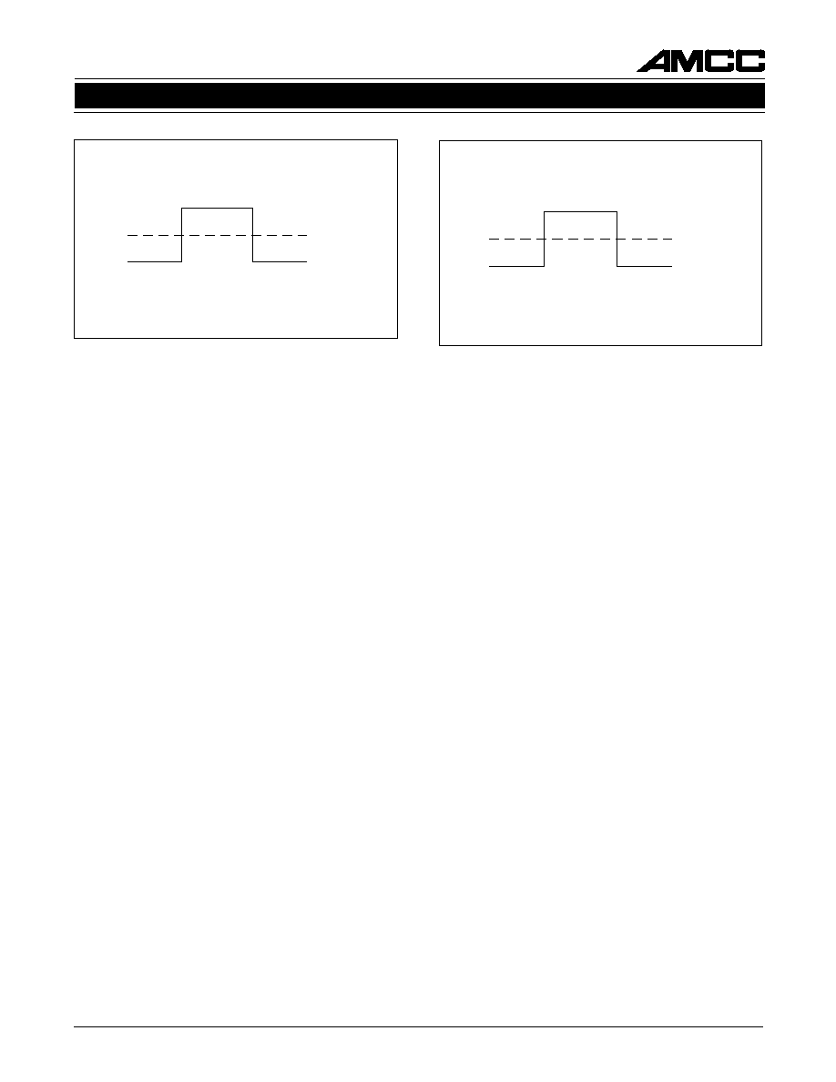
Figure 4. LVECL Signal Waveform
5
EV3019
SONET/SDH/ATM STS-12 TRANSCEIVER EVALUATION BOARD
September 22, 1999
SMA Connectors
SMA connectors are provided for the differential serial
data input/output signals and output clocks. Additional
SMA connectors are provided for an optional differen-
tial serial input clock, the external TTL reference clock
and the optional external parallel input clock.
Receive Serial Data [RSDP/N] -- Differential
LVPECL inputs. Serial data inputs of the S3019.
Receive Serial Clock [RSCLKP/N] -- Differential
LVPECL inputs. These inputs are used in bypass
mode to supply a clock input for the RSDP/N. This
should be tied to a logic zero when not in bypass
mode.
Transmit Serial Data Out [TSDP/N] -- Differential
LVPECL outputs. The serial output data stream from
the transmitter section of the S3019. The outputs can
drive PECL, ECL, or ground terminated instrument
inputs depending on the power supply voltages ap-
plied to the S3019 evaluation board.
Transmit Clock Output [TSCLKP/N] -- Differential
LVPECL outputs. The transmit serial clock that can
be used to re-time the TSDP/N signal. The outputs
can drive PECL, ECL, or ground terminated instru-
ment inputs depending on the power supply voltages
applied to the S3019 evaluation board. This clock will
be 622.08 MHz or 155.52 MHz, depending on the oper-
ating mode.
Reference Clock [REFCLKP/N] -- Differential
LVPECL inputs. These inputs must be provided with
a differential level (depending on the power supply
voltages) clock of 19.44 MHz, 38.8 MHz, 51.84 MHz
or 77.76 MHz as selected by the MODE[1:0] switches
of the DIP switch. These inputs must be connected to a
logic one state (REFCLKP = "1", & REFCLKN = "0" ) if
TTLREF is used.
TTL Reference Clock [TTLREF] -- LVTTL input.
These inputs must be provided with a TTL (swing
levels dependent on the power supply voltages) clock
of 19.44 MHz, 38.88 MHz, 51.84 MHz or 77.76 MHz
as selected by the MODE[1:0] switches of the DIP
switch. These inputs must be tied high if REFCLKP/N
is used.
Parallel I/O Header Terminals
The parallel input (PIN[7:0]) and output (POUT[7:0])
data to and from the S3019 transceiver are available
at a 4 x 9 pin header array at the right edge of the
evaluation board. Ground pin columns are also pro-
vided to allow connection with 0.1" grid shielded rib-
bon cable to parallel data sources and data analyzers.
User selectable jumpers also allow the parallel output
data (POUT[7:0]) and the output byte clock (POCLK)
to be directly connected to the transmitter parallel
data inputs (PIN[7:0]) and the Parallel Input Clock
(PICLK). Note: The board must be supplied with an
external reference via REFCLKP/N for proper opera-
tion. (See Figure 2.)
Parallel Clock [PCLK] -- LVTTL output. The word
rate output reference from the transmitter PLL. This
output is used to coordinate byte-wide transfers via
the parallel data bus.
A separate 5-pin header is also provided for four addi-
tional signals. The four signals are identified below:
19 MHz Clock Output [T19MCLK] -- LVTTL output.
A 19.44 MHz output derived from the S3019 PLL
available at the header pin for monitoring.
38 MHz Clock Output [T38MCLK] -- LVTTL output.
A 38.88 MHz output derived from the S3019 PLL
available at the header pin for monitoring.
Termination = 50
to GND
LSECL
VCC = +2V
+1.2V
+0.7V
+0.2V
VEE = -1.3V +/- 5%
LVPECL
VCC = +3.3V +/- 5%
2.5V
2V
1.5V
VEE = 0V
Termination = 50
to (VCC -2V)
Figure 5. LSECL Signal Waveform
Figure 6. LVPECL Signal Waveform