 | –≠–ª–µ–∫—Ç—Ä–æ–Ω–Ω—ã–π –∫–æ–º–ø–æ–Ω–µ–Ω—Ç: S4405B-66 | –°–∫–∞—á–∞—Ç—å:  PDF PDF  ZIP ZIP |

Applied Micro Circuits Corporation
6195 Lusk Blvd., San Diego, CA 92121 ∑ (619) 450-9333
Page
1
FEATURES
∑ Generates outputs from 10 MHz to 66 MHz
∑ Four groups of three outputs (12 outputs total)
∑ Eight user-selectable output functions for each
group
∑ TTL compatible outputs, with <1.5-ns edge rates
∑ Performs clock doubling, dividing, invert, lead/lag
placement
∑ Internal VCO running between 160 to 266 MHz
∑ 1.0
µ
BiCMOS technology
∑ Output skew less than 500 ps
∑ 52 PQFP package
APPLICATIONS
∑ High-performance microprocessor systems
∑ CMOS ASIC systems
∑ Backplane clock deskew and distribution
∑ Compatible with Intel's PentiumTM processor
GENERAL DESCRIPTION
The S4406 BiCMOS clock generator provides 12 TTL
outputs with less than 500 ps of skew. Implemented
in AMCC's 1.0
µ
BiCMOS technology, the internal
PLL and divider/delay selector logic allow the user to
individually tailor the (4) TTL output groups to the
system's needs. The internal VCO can operate be-
tween 160 to 266 MHz, and the programmability al-
lows the user to generate output clocks in the 20≠66
MHz range.
The S4406 offers the user the ability to select the
appropriate phase and frequency relationship for
each of the four groups of three TTL clock outputs.
In addition to clock doubling and inversion functions,
the S4406 allows any output groups to lead or lag the
others by the minimum phase delay of 3.75≠6.25 ns.
Figure 1. S4406 Block Diagram
PHASE
DETECTOR
CHARGE
PUMP
VCO
I
0
I
1
MUX
REFCLK
FBCLK
TSTEN
0 MS2,1,0
DIVIDE
BY 2 OR 4
DELAY
GENERATION
LOGIC
0 FOUT 0
MODE
SELECTION 1
FILTER
Digital
+5V
0V
Analog
+5V
0V
˜ 2
0 FOUT 1
0 FOUT 2
1 MS2,1,0
1 FOUT 0
MODE
SELECTION 2
1 FOUT 1
1 FOUT 2
2 MS2,1,0
2 FOUT 0
MODE
SELECTION 3
2 FOUT 1
2 FOUT 2
3 MS2,1,0
3 FOUT 0
MODE
SELECTION 4
3 FOUT 1
3 FOUT 2
3
3
3
3
disable
disable
disable
disable
S
DEVICE SPECIFICATION
Æ
12-OUTPUT BiCMOS PLL CLOCK GENERATOR
S4406
Applied Micro Circuits Corporation
6195 Lusk Blvd., San Diego, CA 92121 ∑ (619) 450-9333
Page 2
S4406
FUNCTIONAL DESCRIPTION
xMS2,1,0
MODE DESCRIPTION
xFOUT0,1,2
000
Disabled.
Logical Hi
001
All three outputs at the
f ≠ t
fundamental output freq-
uency, but early by a
minimum phase delay.
010
All three outputs at half
I
/2
the fundamental output
frequency and inverted.
011
All three outputs at the
I
fundamental output freq-
uency and inverted.
100
All three outputs at half
f/2 + t
the fundamental output
frequency, but delayed
by a minimum phase delay.
101
All three outputs at the
f + t
fundamental output freq-
uency, but delayed by a
minimum phase delay.
110
All three outputs at half
f/2
the fundamental output
frequency.
111
All three outputs at the
f
fundamental output
frequency.
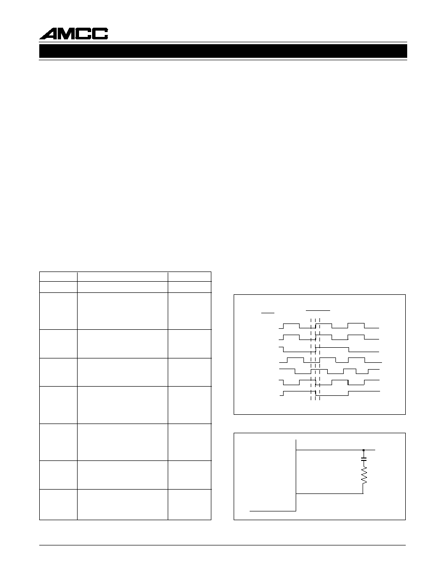
Table 1. Mode Selection Options
Note: If f is fed back, the fundamental frequency is equal to REFCLK.
If f/2 is fed back, the fundamental frequency is twice REFCLK.
110, and the third group (2MS2,1,0) to 101. In this
configuration, one of the 33-MHz outputs should be
fed back to the FBCLK input. This example makes
use of only three of the four output banks, leaving the
fourth available for any other clock signals needed.
Filter
FILTER is the analog signal from the phase detector
going into the VCO. This pin is provided so a simple
external filter (a single capacitor and resistor) can be
included in the phase locked loop of the clock gen-
erator. See Figure 3.
Phase Delay
The minimum phase delay between xFOUT0≠2 sig-
nals is a function of the VCO frequency. The VCO
frequency can be determined by multiplying the fun-
damental output frequency by four, or half the funda-
mental frequency by eight. The minimum phase
delay is equal to the period of the VCO frequency: t =
1/(VCO freq). Since the VCO can operate in the 160-
MHz to 266-MHz range, the range of minimum phase
delay values is 6.25 ns to 3.75 ns (See Table 2).
FUNCTIONAL DESCRIPTION
The 12 xFOUT0≠2 outputs are the main TTL output
clocks that the generator supplies. The mode selec-
tion choices are shown in Table 1 and waveform defi-
nitions are given in Figure 2. The "x" represents the
output group number (1≠4). The frequency of these
outputs is determined by the REFCLK clock fre-
quency and the output clock that is tied to the FBCLK
input (xFOUT0≠2 can be equal to REFCLK, half of
REFCLK, or twice the frequency of REFCLK).
Example:
In order to meet bus timing specifications for a typical
system, designers may need three outputs at 66 MHz
for the system clock and processor, a 33-MHz output
for the cache controller, and a 33-MHz delayed out-
put for a memory management unit. This system re-
quirement can be met using the S4406 by setting the
mode select pins for the first group of outputs
(0MS2,1,0) to 111, the second group (1MS2,1,0) to
Figure 2. Waveform Definitions
Figure 3. External PLL Filter
A +5V
.1 µF
1.5k
43
42
S4406
A VCC
FILTER
f
f/2
f + t
REFCLK
Table
entry
Waveform
f ≠ t
I
I
/2
≠t 0 t
Applied Micro Circuits Corporation
6195 Lusk Blvd., San Diego, CA 92121 ∑ (619) 450-9333
Page
3
BOARD LAYOUT
S4406
Test Capabilities
TESTEN allows the chip to use the REFCLK input
instead of the VCO output to clock the chip. This is
used during chip test to allow the counters and con-
trol logic to be tested independently of the VCO. In
addition, when TESTEN is brought High, an internal
RESET pulse is generated. This initializes the inter-
nal counter flip-flops to zeros, and at the end of the
next clock cycle, the outputs go to a zero state.
TESTEN can also be used for board testing to allow
the user to control the output clocks from the S4406
by inputting the board clock to the REFCLK input.
tors capable of handling 25 mA. The recommended
value for the inductors is in the range from 5 to
100
µ
H, and depends upon the frequency spectrum of
the digital power supply noise.
Decoupling capacitors are also very important to mini-
mize noise. The decoupling capacitors must have low
lead inductance to be effective, so ceramic chip capaci-
tors are recommended. Decoupling capacitors should
be located as close to the power pins as physically
possible. And the decoupling should be placed on the
top surface of the board between the part and its con-
nections to the power and ground planes.
BOARD LAYOUT CONSIDERATIONS
∑ The S4406 chips are sensitive to noise on the Ana-
log +5 V and Filter pins. Care should be taken during
board layout for optimum results.
∑ All decoupling capacitors (C1≠C4 = 0.1
µ
F) should
be bypassed between VCC and GND, and placed as
close to the chip as possible (preferably using ce-
ramic chip caps) and placed on top of board between
S4406 and the power and ground plane connections.
∑ No dynamic signal lines should pass through or
beneath the filter circuitry area (enclosed by dashed
lines in Figure 5) to avoid the possibility of noise due
to crosstalk.
∑ The analog VCC supply can be a filtered digital
VCC supply as shown below. The ferrite beads or
inductors, FB1 and FB2, should be placed within
three inches of the chip.
∑ The analog VCC plane should be separated from
the digital VCC and ground planes by at least 1/8
inch.
VCO
MIN PHASE
xFOUT0≠2
FREQ
DELAY
66.6 MHz
266 MHz
3.750 ns
50 MHz
200 MHz
5.000 ns
40 MHz
160 MHz
6.250 ns
33.3 MHz
266 MHz
3.750 ns
25 MHz
200 MHz
5.000 ns
20 MHz
160 MHz
6.250 ns
Table 2. VCO Operating Frequencies
The bank containing the output used as feedback
must be in one of the f/2 modes to ensure the VCO is
operating within its 160-266 MHz range.
Power Supply Considerations
Power for the analog portion of the S4406 chips must
be isolated from the digital power supplies to mini-
mize noise on the analog power supply pins. This
isolation between the analog and digital power sup-
plies can be accomplished with a simple external
power supply filter (Figure 4). The analog power
planes are connected to the digital power planes
through single ferrite beads (FB1 and FB2) or induc-
Figure 4. External Power Supply Filter
ANALOG +5V
0.1 µF
DIGITAL +5V
DIGITAL GND
ANALOG GND
FB1
FB2
10 µF
Tantalum
(optional)
45
44
43
42
1.5K
0.1
µ
F
0.1
µ
F
A +5V
D GND
D +5V
FB2
FB1
S4406
A GND
Figure 5. Board Layout

Applied Micro Circuits Corporation
6195 Lusk Blvd., San Diego, CA 92121 ∑ (619) 450-9333
Page 4
PIN DESCRIPTIONS
Input Signals
REFCLK. Frequency reference supplied by the user
that, along with the output tied to the FBCLK input,
determines the frequency of the outputs. Also re-
places the VCO output when TSTEN is high (after
first divide-by-two stage in divider phase control
logic). See TSTEN.
FBCLK. Feedback clock that, along with the REFCLK
input, determines the frequency of the outputs. One
output is selected to feed back to this input.
TSTEN. Active High. Allows REFCLK to drive the
divider phase adjust circuitry, after the first divide-by-
two stage. Also, when brought High, generates an
internal Reset pulse that initializes the internal
counter flip-flops to zero.
xMS2,1,0. Mode selection inputs that allow selection
of the phase and frequency relationship of each of
the four banks of three clock outputs. The "x" repre-
sents the output group number (0≠3). Refer to Table
1 for mode selection options.
Output Signals
FILTER. A tap between the analog output of the
phase detector and the VCO input. Allows a simple
external filter (a single resistor and one capacitor) to
be included in the PLL.
xFOUT0≠2. Clock signal outputs. Refer to Table 1
and Figure 4 for a description of output options.
S4406
PIN DESCRIPTIONS
Applied Micro Circuits Corporation
6195 Lusk Blvd., San Diego, CA 92121 ∑ (619) 450-9333
Page
5
ELECTRICAL CHARACTERISTICS/PACKAGING
S4406
Symbol
VIH2
Input HIGH Voltage
2.0
2.4
2.0
-25
V
Guaranteed input HIGH voltage for all inputs
VIL2
Input LOW Voltage
VIK
Input clamp diode voltage
0.8
V
-1.2
0.5
-0.8
V
V
V
V
µA
µA
Guaranteed input LOW voltage for all inputs
VCC = Min, IIN = -18 mA
II
Input HIGH Current at Max
1.0
mA
50
VCC = Max, VIN = VCC
IOS4
Output short circuit current
-100
-200
mA
VCC = Max, VOUT = 0V
ICC
Static
70
mA
VCC = Max
ICCT
Total ICC (Dynamic and Static)
200
mA
CLOAD = 25 pF at 50 MHz
IIH
Input HIGH Current
VCC = Min, VIN = 2.4V
VCC = Min, VIN = 0.5V
VOH
Output HIGH Voltage
VCC = Min
VOL
Output LOW Voltage
VCC = Min,
IIL
Input LOW Current
IOH = -12 mA3
IOH = -24 mA3
Parameter
Min
Typ1
Max
Units
DC Test Conditions
4MS2,3MS2,1,0
Other
µA
µA
-50
-500
4MS2,3MS2,1,0
Other
IOL = 24 mA3
DC CHARACTERISTICS
1. Typical limits are at 25
∞
C, V
CC
= 5.0V.
2. These input levels provide zero noise immunity and should only be tested in a static, noise-free environment.
3. I
OH
/I
OL
values indicated are for DC test correlation. Actual dynamic currents are significantly higher.
4. Maximum test duration one second.
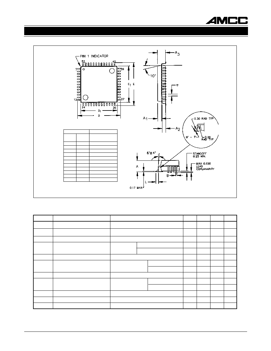
Figure 6. 52≠pin PQFP Package
All dimensions in mm.
BODY SIZE PLUS 3.2 MM FOOTPRINT
DIM
LTR
e
B
A
A1
A2
A3
D
D1
E
E1
L
TOL/
LEADS
TYP
TYP
MAX
±.10
±.10
±.10
±.25
±.10
±.25
±.10
±.15/.10
52
1.00
.35
2.45
.920
.920
2.00
17.20
14.00
17.20
14.00
.88