 | –≠–ª–µ–∫—Ç—Ä–æ–Ω–Ω—ã–π –∫–æ–º–ø–æ–Ω–µ–Ω—Ç: S4505 | –°–∫–∞—á–∞—Ç—å:  PDF PDF  ZIP ZIP |

Applied Micro Circuits Corporation
6195 Lusk Blvd., San Diego, CA 92121 ∑ (619) 450-9333
Page 1
S4505/06/07
RAMBUSTM COMPATIBLE CLOCK GENERATORS
S4505/06/07
RAMBUSTM COMPATIBLE CLOCK GENERATORS
Æ
FEATURES
∑ Provides two Rambus compatible clock outputs
from 240 to 310 MHz
∑ Uses low cost 14.318 MHz crystal as reference
for 250 MHz output
∑ Low Jitter, <100 ps
∑ Output skew <50ps
∑ 45/55% duty cycle
∑ On-chip filter requires no external components
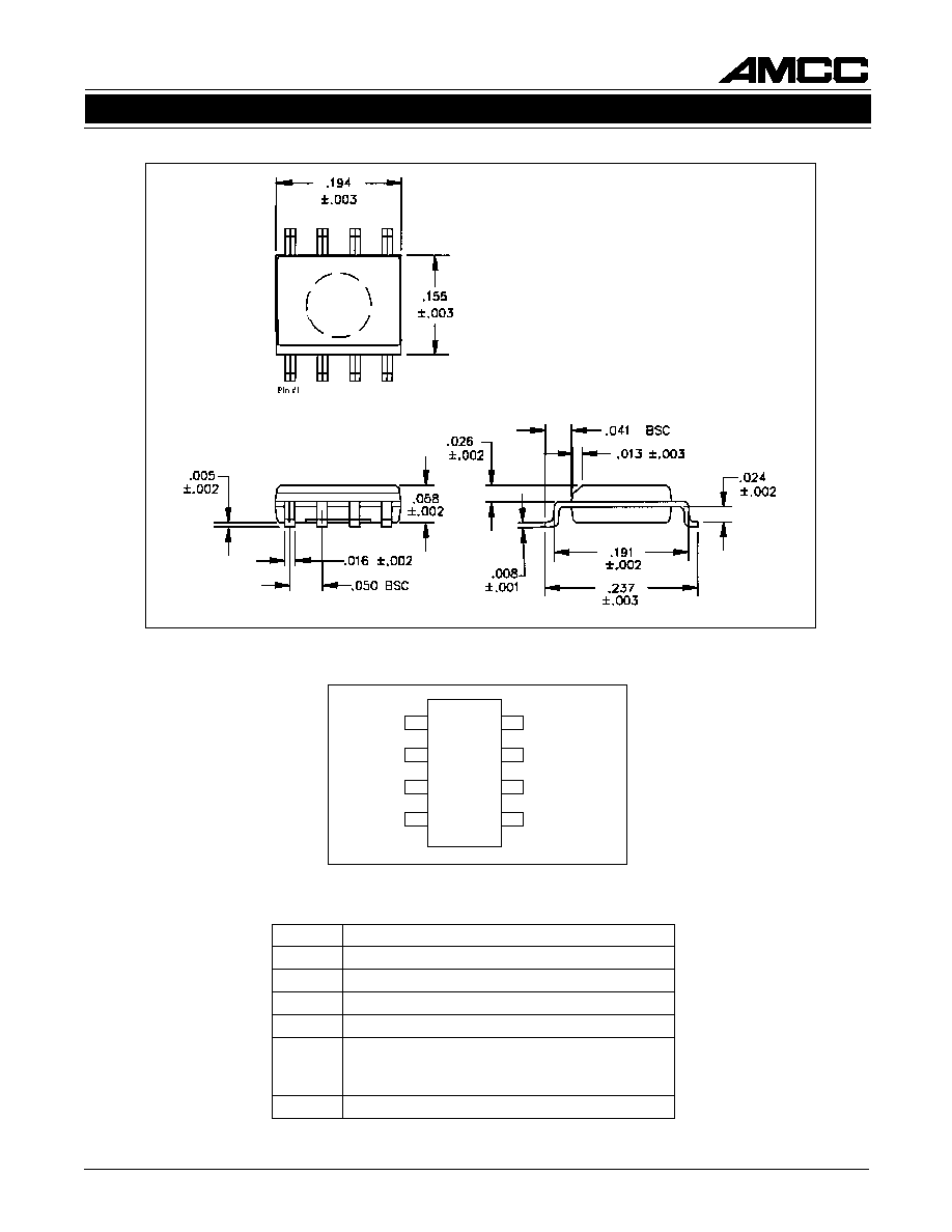
∑ Eight-pin, .150" SOIC
∑ Operates from a single 3.3V
±
10% supply
∑ Series resonant input crystal requires no
external components
APPLICATIONS--RDRAM BASED
∑ Graphics Accelerators
∑ PC Memory
∑ Set-Top Boxes
∑ Games
DESCRIPTION
AMCC's advanced PLL technology allows the S4505
to provide two Rambus-compatible, 250, 267, or 300
MHz clocks from a low cost 14.318 MHz crystal.
Other reference crystals can be used to produce
other output frequencies within the 240≠310 MHz
range. An external series resistor allows the output
to be matched to the Rambus transmission line im-
pedance needed for each application.
AMCC utilizes its high speed, low-jitter PLL technol-
ogy developed for telecom and precision clocking
applications to provide outputs which meet the low
jitter and symmetrical duty cycle requirements of
RAMBUS system clocks.
PRELIMINARY
DEVICE SPECIFICATION
Phase Detector
Active Filter
and VCO
N
Divider
XTAL
OSC
Feedback
XTAL0
XTAL1
OE
VDD
GND
240≠310 MHz
Output A
240≠310 MHz
Output B
Ref
M
Divider
Block Diagram

Applied Micro Circuits Corporation
6195 Lusk Blvd., San Diego, CA 92121 ∑ (619) 450-9333
Page 2
RAMBUSTM COMPATIBLE CLOCK GENERATORS
S4505/06/07
Parameter
Description
Value
Unit
V
DD
Power supply vs. GND
-0.5 to +5.0
V
V
IN
Storage Temp.
Input voltage, and pin vs. GND
-0.5 to V
DD
+0.5
V
Maximum temperature during storage
170∞
∞C
Absolute Maximum Ratings
Note: Stresses greater than the absolute maximum ratings may cause permanent damage to the device. Functional operation of the
device at these or any other conditions above those indicated under the normal operating conditions is not guaranteed. Exposure to
absolute maximum rating conditions for extended periods may affect device reliability.
Parameter
Description
Conditions
Min
Max
Unit
V
IH
Input HIGH voltage
OE Pin
2.0
V
V
IL
I
IH
Input LOW voltage
OE Pin
0.8
V
I
IL
Input HIGH current
OE Pin
50
uA
P
D
Input LOW current
OE Pin ≠ Internal pull-up
300
uA
Power Dissipation
Dynamic
440
mW
Symbol
Description
Comments
Min
Typ
Max
Unit
Z
0
Line impedance
Rambus compatible
25
50
V
S
V
ACO
Output voltage swing
Rambus compatible
1.2
1.6
V
Output Asymmetry
Rambus compatible
-15
+15
%
Output Characteristics
All specifications are compatible with Rambus requirements.
DC Specifications (T
A
= 0∞C ≠ 70∞C, V
DD
= 3.3
±
0.3V)
Symbol
Description
Test Condition
Min
Typ
Max
Unit
F
XTAL
Crystal frequency
12.86
14.318
14.46
MHz
F
OUT
Output frequency,S4507
Typ with 14.318 MHz input
1
310
240
300
MHz
T
R,
T
F
T
DC
Output clock rise/fall time
20% to 80%
0.2
0.5
ns
Duty cycle
45
50
55
%
T
JPP
Jitter, peak-to-peak
40
100
ps
T
PU
Power-up time
From OFF to clocks stable
STD Rambus System Load
10
ms
T
SKEW
Output A to B skew
Equal loads
50
ps
F
OUT
Output frequency,S4506
Typ with 14.318 MHz input
1
310
240
250
MHz
F
OUT
Output frequency,S4505
Typ with 14.318 MHz input
1
310
240
267
MHz
20
AC Specifications (Operating Conditions: T
A
= 0∞C ≠ 70∞C, V
DD
= 3.3V
±
0.3V)
All specifications are compatible with Rambus requirements.
1. Output frequency multiplier is 35/2 times the input crystal frequency on the S4506, 56/3 times the input crystal frequency on the S4505,
and 21 times the input crystal frequency on the S4507.
Applied Micro Circuits Corporation
6195 Lusk Blvd., San Diego, CA 92121 ∑ (619) 450-9333
Page 3
S4505/06/07
RAMBUSTM COMPATIBLE CLOCK GENERATORS
VDD
1
OE
XTAL1
XTAL0
GND
8
7
6
5
OUTPUT B
GND
OUTPUT A
2
3
4
S4505/06/07 Pinout -- 8-Pin SOIC
Pin #
Description
1
Output enable, Active HIGH, Internal pull-up
2
3
Crystal connection -- Series Resonant
4, 6
Crystal connection -- Series Resonant
5, 7
Ground
8
Output A, B -- 240≠310 MHz clock outputs,
open drain -- should be terminated
externally to match Rambus specifications
Power -- 3.3V
±
10%
Pin Descriptions
8-pin SOIC

Applied Micro Circuits Corporation
6195 Lusk Blvd., San Diego, CA 92121 ∑ (619) 450-9333
Page 4
RAMBUSTM COMPATIBLE CLOCK GENERATORS
S4505/06/07
AMCC is a registered trademark of Applied Micro Circuits Corporation.
Copyright Æ 1997 Applied Micro Circuits Corporation
March 10, 1997
AMCC reserves the right to make changes to its products or to discontinue any semiconductor product or service without notice, and
advises its customers to obtain the latest version of relevant information to verify, before placing orders, that the information being relied
on is current.
AMCC does not assume any liability arising out of the application or use of any product or circuit described herein, neither does it
convey any license under its patent rights nor the rights of others.
AMCC reserves the right to ship devices of higher grade in place of those of lower grade.
AMCC SEMICONDUCTOR PRODUCTS ARE NOT DESIGNED, INTENDED, AUTHORIZED, OR WARRANTED TO BE SUITABLE FOR
USE IN LIFE-SUPPORT APPLICATIONS, DEVICES OR SYSTEMS OR OTHER CRITICAL APPLICATIONS.
Applied Micro Circuits Corporation ∑ 6195 Lusk Blvd., San Diego, CA 92121
Phone: (619) 450-9333 Fax: (619) 450-9885
http://www.amcc.com
AMCC products are available in several shipping configurations.
The order number is formed by a combination of:
∑ Device Number
∑ Package Type
∑ Optional Shipping Configuration
S450x
S
/TD
Optional Shipping Configuration
Blank = 92-unit tube (for 8-pin SOIC)
/D = dry pack
/TD = tape, reel and dry pack
Package Option
S = 8-pin SOIC
Device Number
Example: S4506S/D
8-pin SOIC package, shipped dry packed in tubes.
Ordering Information