
Æ
Features
Part Number S4803
Revision 1.6 - July 2000
General Description
YUKON
STS-48c POS/ATM SONET MAPPER
S4803 Block Diagram
AMCC
ADVANCED SUMMARY DATASHEET
Advanced Information - The information contained in this
document is about a product in its design phase and is subject
to change without notice at any time. All features described
herein are design goals. Contact AMCC for updates to this
document and the latest product status.
∑ Complies with ANSI, Bellcore and ITU-T specifica-
tions for Jitter Tolerance, Transfer and Generation.
∑ SONET/SDH Mapper with Integrated serializer/dese-
rializer provides direct connection to fiber optic trans-
ceivers via a differential CMI Interface at 2.48Gbit/s.
∑ On chip high frequency PLLs for clock recovery sup-
porting OC-48 rate using a 155.52 Mhz ref. clock.
∑ Processes SONET/SDH STS-48c/(STM-16/AU-4-
16c) data streams with full duplex mapping of ATM
cells or packets (PPP or LAPS) into SONET/SDH
payloads.
∑ Terminates and generates SONET/SDH section, line,
and path layers, with transport/section E1, E2, F1 and
DCC overhead serial interfaces in both transmit and
receive directions.
∑ Provides a 32-bit parallel system-side interface oper-
ating at 100 MHz.
∑ Selectable scrambling/descrambling (1+X
6
+X
7
) of
SONET/SDH frame.
∑ Selectable self-synchronous scramblers (before or
after the ATM/HDLC processors) implementing (X
43
+1) polynomial for ATM or POS applications.
∑ Generic 8-bit microprocessor interface for configura-
tion, control, and status monitoring.
∑ Provides IEEE 1149.1 JTAG (boundary scan) test port
∑ Implemented in 3.3V technology, 352 pin SBGA.
The S4803 is a highly-integrated VLSI device that pro-
vides full-duplex mapping of PPP/LAPS encapsulated
packets or ATM cells into SONET/SDH payloads. The
S4803 includes an integrated OC48 transceiver with
CRU (clock recovery unit) which provides a direct con-
nection to a fiber optic transceiver.
The S4803 provides full section, line, and path overhead
processing and supports framing, scrambling/descram-
bling, alarm signal insertion/detection, and bit inter-
leaved parity (B1/B2/B3) processing.
The S4803 is standards compliant with Bellcore GR-
253, ITU G.707, ANSI T1.105 -1995, IETF RFCs 1619/
1661/1662/2615 (PPP) and ITU-T COM 7-224-E/D307
(LAPS recommendation) protocols.
A general purpose 8-bit microprocessor interface is pro-
vided for control, and monitoring. The interface supports
both Intel and Motorola type microprocessors, and is
capable of operating in either an interrupt driven or
polled-mode configurations.
Applications
∑
ATM switches
∑
Packet over SONET Routers and Switches
∑
SONET/SDH Add Drop Multiplexers, Terminal
Multiplexers and Digital Cross Connects
∑
Test equipment
U
T
OP
I
A
-
3
o
r
F
l
e
x
B
U
S
-
3
TM
INT
E
RF
A
C
E
TX_SYS_DAT[31:0]
TX_CLK
TX_PRTY
TX_ENB
TX_SOC/P
TX_CLAV/PA
RX_SYS_DAT[31:0]
RX_CLK
RX_PRTY
RX_ENB
RX_SOC/P
RX_CLAV/PA
RX ATM/
PROC
POINTER
INTERPRET
POH
MONITOR
TOH EXTRACT
TOH
MONITOR
RX
FRAMER
L
I
NE S
I
DE
INT
E
RF
ACE
TX
FRAMER
TOH INSERT
SPE/VC
GENERATE
T
X
S
DCCDA
T
A
T
X
SDCCCL
K
T
X
L
D
CCDA
T
A
T
X
L
DCCCL
K
T
XE1
E2
F
1
FRAM
E
TX
E1
E2
F
1
D
A
T
RX
SDCCDA
T
A
RX
SDCCCL
K
RX
L
DCC
DA
T
A
RXL
DCCCL
K
R
X
E
1
E2
F1
F
R
AM
E
RX
E1
E2
F1
DA
T
RX_RVAL
RX_VBYTE[2:0]
RX_EOP
RX_ERR
TX_VBYTE[2:0]
TX_EOP
TX_ERR
D
[
7:
0]
A
DDR[1
1
:0
]
CSN
RDB(
D
SB
)
WRB(
R
W
B
)
RDY
B(
DT
ACKB
)
BU
S
M
O
D
E
INT
B
MICROPROCESSOR I/F
JTAG PORT
GPIO/LED REG
TD
O
TD
I
TC
K
TM
S
TR
S
T
B
GP
IO[7
:0]
TSDP/TSDN
T
X
8K
CLK
RS
T
B
A
PS_
I
N
T
B
TS
_E
N
RX_LOSEXT
RX
FIFO
DE-SCRMBL
(X
43
+ 1)
RX ATM/
CNTRS
TX
FIFO
DE-SCRMBL
(X
43
+ 1)
SCRMBL
(X
43
+ 1)
TX ATM/
HDLC(PPP/LAPS)
PROC
SCRMBL
(X
43
+ 1)
RX_ALRM_OUT
RX_CLK_OUT
RSDP/RSDN
DLE
B
REF
C
L
KP/
TSCLKP/TSCLKN
LL
E
B
REF
C
L
K
N
HDLC(PPP/LAPS)
HDLC(PPP/LAPS)
PRELIMINARY PRODUCT DATASHEET
AMCC
AMCC, 6290 Sequence Drive, San Diego, CA 92121-4358. Ph: 800-755-2622 Fax:619-450-988
S4803 STS-48c POS/ATM SONET MAPPER
Revision 1.6 - July 2000
ADVANCED SUMMARY DATASHEET
Overview and Applications
SONET Processing
The S4803 implements SONET/SDH processing and
full-duplex ATM/POS mapping functions for STS-48/
STM-16 data streams. It supports a single STS-48c/AU-
4-16c signal within an STS-48/STM-16. A TOH/SOH
interface provides direct add/drop capability for E1, E2,
F1, and both Section and Line DCC channels. The
S4803 also includes a clear channel mode that enables
the direct transmission of system payload from the sys-
tem interface to the line-side interface.
On the transmit side the S4803 generates section, line,
and path overhead. It performs framing pattern insertion
(A1, A2), scrambling, alarm signal insertion, and gener-
ates section, line and path Bit Interleaved Parity (B1/B2/
B3) for far-end performance monitoring.
On the receive side the S4803 processes section, line,
and path overhead. It performs framing (A1, A2),
descrambling, alarm detection, Pointer Interpretation, Bit
Interleaved Parity monitoring (B1/B2/B3), and error
count accumulation for performance monitoring.
ATM Processing
When configured for ATM cell processing, the S4803's
transmit ATM processor will perform all necessary cell
encapsulation including HEC generation, cell payload
scrambling (X
43
+1) and idle cell insertion to adapt the
cell rate to the SPE. When receiving data from the line
side, it performs cell delineation, Rx header error correc-
tion/detection, descrambling, and detects & deletes idle
cells.
Packet/HDLC Processing
When configured for POS mode, the S4803's transmit
HDLC processor provides the insertion of HDLC framed
PPP/LAPS packets into the STS SPE. It will perform
packet framing, inter-frame fill and Tx FIFO error recov-
ery. In addition, it optionally performs scrambling
(X
43
+1), either pre or post the HDLC processor, per-
forms transparency processing as required by RFC
1662/ITU-T COM7-D307 and will optionally generate a
16/32 bit FCS (if enabled).
The receive HDLC processor provides for the extraction
of PPP/LAPS packets from HDLC frames, transparency
removal, de-scrambling (if enabled), FCS error check-
ing, and optionally deletes the HDLC address and con-
trol fields.
Line-side Interface
On the line-side, the S4803 supports a serial LVPECL
interface operating at 2.48GHz. The S4803 is typically
connected to an electrical-to-optical converter for inter-
facing to the fiber optic interface. (See figure below.) The
clock synthesis function requires a 155MHz reference
clock for phase locked loop startup and proper operation
during LOS conditions. In the transmit direction this ref-
erence clock is used to synthesize the output data rate
and must therefore be less than 20ppm accuracy.
System Interface
The S4803 supports a 32 bit, 100 MHz system interface.
When operating in ATM mode, the S4803 supports the
32-bit, 100 MHz, Utopia Level-3 interface. When operat-
ing in POS mode, the S4803 supports a 32-bit, 100
MHz, FlexBUS-3
TM
interface.
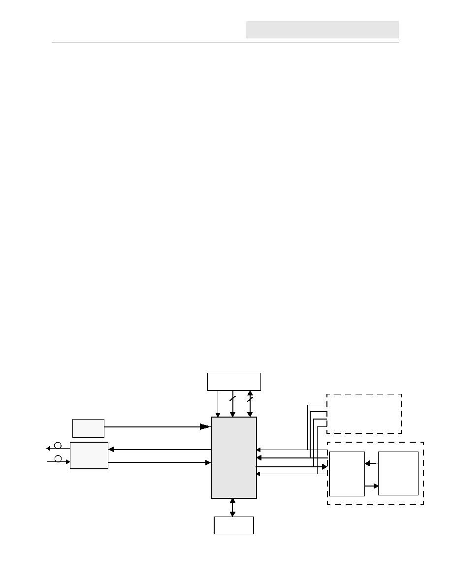
TYPICAL APPLICATIONS: S4803 in 2.488 Mb/s ATM or POS System
RSDP/N
TSDP/N
Microprocessor
Control
Control
Reference
Clock
Fiber Optic
Transceiver
SONET
Line Side
Interface
S4803
AMCC
Addr
Data
8
12
TX_CLK
TX_SYS_DAT[31:0]
RX_CLK
RX_SYS_DAT[31:0]
Utopia Level-3 or POS 32-bit
System Interface
TOH Insertion
and Extraction
IP Router or ATM Switch
OR
Multi
Channel
Link Layer
Device
IP ROUTER
Switching/
Routing
Logic
Lucent 1417K4A
[31:0]
[31:0]
OC-48
Line Interface
REFCLKP/N
(No Clock Rec)
155Mhz