
ADVANCE INFORMATION
This document contains information on a product under development at Advanced Micro Devices. The information
is intended to help you evaluate this product. AMD reserves the right to change or discontinue work on this proposed
product without notice.
Publication# 21525
Rev: A Amendment/0
Issue Date: January 1998
Refer to AMD's Website (www.amd.com) for the latest information.
Am29LV081B
8 Megabit (1 M x 8-Bit)
CMOS 3.0 Volt-only Sector Erase Flash Memory
DISTINCTIVE CHARACTERISTICS
s
Optimized architecture for Miniature Card and
mass storage applications
s
Single power supply operation
-- Full voltage range: 2.7 to 3.6 volt read and write
operations for battery-powered applications
-- Regulated voltage range: 3.0 to 3.6 volt read and
write operations and for compatibility with high
performance 3.3 volt microprocessors
s
Manufactured on 0.35
µ
m process technology
-- Compatible with 0.5
µ
m Am29LV081 device
s
High performance
-- Full voltage range: access times as fast as 80 ns
-- Regulated voltage range: access times as fast
as 70 ns
s
Ultra low power consumption (typical values at
5 MHz)
-- 200 nA Automatic Sleep mode current
-- 200 nA standby mode current
-- 7 mA read current
-- 15 mA program/erase current
s
Flexible sector architecture
-- Sixteen 64 Kbyte sectors
-- Supports full chip erase
-- Sector Protection features:
A hardware method of locking a sector to
prevent any program or erase operations within
that sector
Sectors can be locked in-system or via
programming equipment
Temporary Sector Unprotect feature allows code
changes in previously locked sectors
s
Unlock Bypass Program Command
-- Reduces overall programming time when
issuing multiple program command sequences
s
Embedded Algorithms
-- Embedded Erase algorithm automatically
preprograms and erases the entire chip or any
combination of designated sectors
-- Embedded Program algorithm automatically
writes and verifies data at specified addresses
s
Minimum 1,000,000 write cycle guarantee per
sector
s
Package option
-- 40-pin TSOP
s
Compatibility with JEDEC standards
-- Pinout and software compatible with single-
power supply Flash
-- Superior inadvertent write protection
s
Data# Polling and toggle bits
-- Provides a software method of detecting
program or erase operation completion
s
Ready/Busy# pin (RY/BY#)
-- Provides a hardware method of detecting
program or erase cycle completion
s
Erase Suspend/Erase Resume
-- Suspends an erase operation to read data from,
or program data to, a sector that is not being
erased, then resumes the erase operation
s
Hardware reset pin (RESET#)
-- Hardware method to reset the device to reading
array data

2
Am29LV081B
A D V A N C E I N F O R M A T I O N
GENERAL DESCRIPTION
The Am29LV081B is an 8 Mbit, 3.0 volt-only Flash
memory organized as 1,048,576 bytes. The device is
offered in a 40-pin TSOP package. The byte-wide (x8)
data appears on DQ7≠DQ0. This device requires only
a single, 3.0 volt V
CC
supply to perform read, program,
and erase operations. A standard EPROM pro-
grammer can also be used to program and erase the
device.
This device is manufactured using AMD's 0.35
µ
m
process technology, and offers all the features and ben-
efits of the Am29LV081, which was manufactured using
0 . 5
µ
m p r o c e s s t e c h n o l o g y. I n a d d i t i o n , t h e
Am29LV081B features unlock bypass programming
and in-system sector protection/unprotection.
The standard device offers access times of 70, 80, 90,
and 120 ns, allowing high speed microprocessors to
operate without wait states. To eliminate bus contention
the device has separate chip enable (CE#), write
enable (WE#) and output enable (OE#) controls.
The device requires only a single 3.0 volt power sup-
ply for both read and write functions. Internally gener-
ated and regulated voltages are provided for the
program and erase operations.
The device is entirely command set compatible with the
JEDEC single-power-supply Flash standard. Com-
mands are written to the command register using
standard microprocessor write timings. Register con-
tents serve as input to an internal state-machine that
controls the erase and programming circuitry. Write
cycles also internally latch addresses and data needed
for the programming and erase operations. Reading
data out of the device is similar to reading from other
Flash or EPROM devices.
Device programming occurs by executing the program
command sequence. This initiates the Embedded
Program algorithm--an internal algorithm that auto-
matically times the program pulse widths and verifies
proper cell margin. The Unlock Bypass mode facili-
tates faster programming times by requiring only two
write cycles to program data instead of four.
Device erasure occurs by executing the erase command
sequence. This initiates the Embedded Erase algo-
rithm--an internal algorithm that automatically prepro-
grams the array (if it is not already programmed) before
executing the erase operation. During erase, the device
automatically times the erase pulse widths and verifies
proper cell margin.
The host system can detect whether a program or
erase operation is complete by observing the RY/BY#
pin, or by reading the DQ7 (Data# Polling) and DQ6
(toggle) status bits. After a program or erase cycle has
been completed, the device is ready to read array data
or accept another command.
The sector erase architecture allows memory sectors
to be erased and reprogrammed without affecting the
data contents of other sectors. The device is fully
erased when shipped from the factory.
Hardware data protection measures include a low
V
CC
detector that automatically inhibits write opera-
tions during power transitions. The hardware sector
protection feature disables both program and erase
operations in any combination of the sectors of mem-
ory. This can be achieved in-system or via program-
ming equipment.
The Erase Suspend feature enables the user to put
erase on hold for any period of time to read data from,
or program data to, any sector that is not selected for
erasure. True background erase can thus be achieved.
The hardware RESET# pin terminates any operation
in progress and resets the internal state machine to
reading array data. The RESET# pin may be tied to the
system reset circuitry. A system reset would thus also
reset the device, enabling the system microprocessor
to read the boot-up firmware from the Flash memory.
The device offers two power-saving features. When ad-
dresses have been stable for a specified amount of
time, the device enters the automatic sleep mode.
The system can also place the device into the standby
mode. Power consumption is greatly reduced in both
these modes.
AMD's Flash technology combines years of Flash
memory manufacturing experience to produce the
highest levels of quality, reliability and cost effective-
ness. The device electrically erases all bits within
a sector simultaneously via Fowler-Nordheim tun-
neling. The data is programmed using hot electron
injection.
Am29LV081B
3
A D V A N C E I N F O R M A T I O N
PRODUCT SELECTOR GUIDE
Note: See "AC Characteristics" for full specifications.
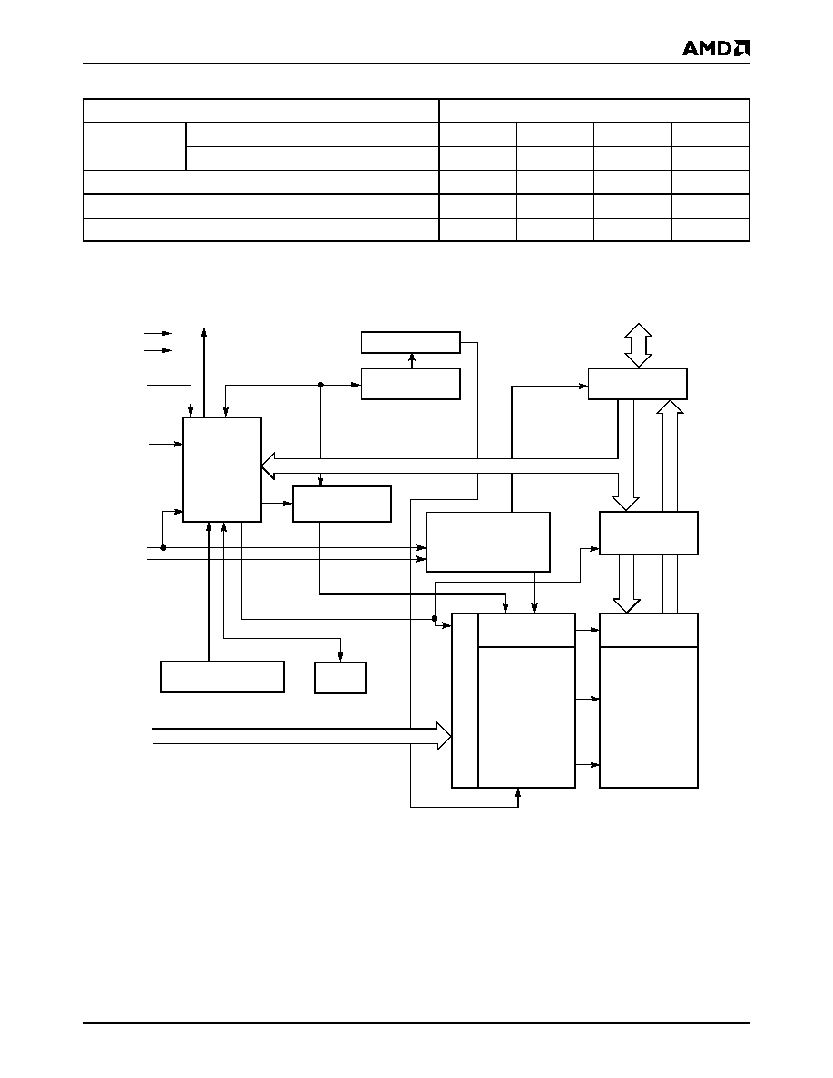
BLOCK DIAGRAM
Family Part Number
Am29LV081B
Speed Options
Regulated Voltage Range: V
CC
=3.0≠3.6 V
-70R
Full Voltage Range: V
CC
= 2.7≠3.6 V
-80
-90
-120
Max access time, ns (t
ACC
)
70
80
90
120
Max CE# access time, ns (t
CE
)
70
80
90
120
Max OE# access time, ns (t
OE
)
30
30
35
50
Input/Output
Buffers
X-Decoder
Y-Decoder
Chip Enable
Output Enable
Erase Voltage
Generator
PGM Voltage
Generator
Timer
V
CC
Detector
State
Control
Command
Register
V
CC
V
SS
WE#
CE#
OE#
STB
STB
DQ0
≠
DQ7
Sector Switches
RY/BY#
RESET#
Data
Y-Gating
Cell Matrix
A
ddr
ess
La
tch
A0≠A19
21525A-1

4
Am29LV081B
A D V A N C E I N F O R M A T I O N
CONNECTION DIAGRAMS
1
16
2
3
4
5
6
7
8
17
18
19
20
9
10
11
12
13
14
15
40
25
39
38
37
36
35
34
33
32
31
30
29
28
27
26
24
23
22
21
A16
A5
A15
A14
A13
A12
A11
A9
A8
WE#
RESET#
NC
RY/BY#
A18
A7
A6
A4
A3
A2
A1
A17
DQ0
V
SS
NC
A19
A10
DQ7
DQ6
DQ5
OE#
V
SS
CE#
A0
DQ4
V
CC
V
CC
NC
DQ3
DQ2
DQ1
1
16
2
3
4
5
6
7
8
17
18
19
20
9
10
11
12
13
14
15
40
25
39
38
37
36
35
34
33
32
31
30
29
28
27
26
24
23
22
21
A16
A5
A15
A14
A13
A12
A11
A9
A8
WE#
RESET#
NC
RY/BY#
A18
A7
A6
A4
A3
A2
A1
A17
DQ0
V
SS
NC
A19
A10
DQ7
DQ6
DQ5
CE#
V
SS
CE#
A0
DQ4
V
CC
V
CC
NC
DQ3
DQ2
DQ1
21525A-2
Reverse TSOP
Standard TSOP
Am29LV081B
5
A D V A N C E I N F O R M A T I O N
PIN CONFIGURATION
A0≠A19
= 20 addresses
DQ0≠DQ7 = 8 data inputs/outputs
CE#
= Chip enable
OE#
= Output
enable
WE#
= Write enable
RESET#
= Hardware reset pin, active low
RY/BY#
= Ready/Busy#
output
V
CC
= 3.0 volt-only single power supply
(see Product Selector Guide for speed
options and voltage supply tolerances)
V
SS
= Device ground
NC
= Pin not connected internally
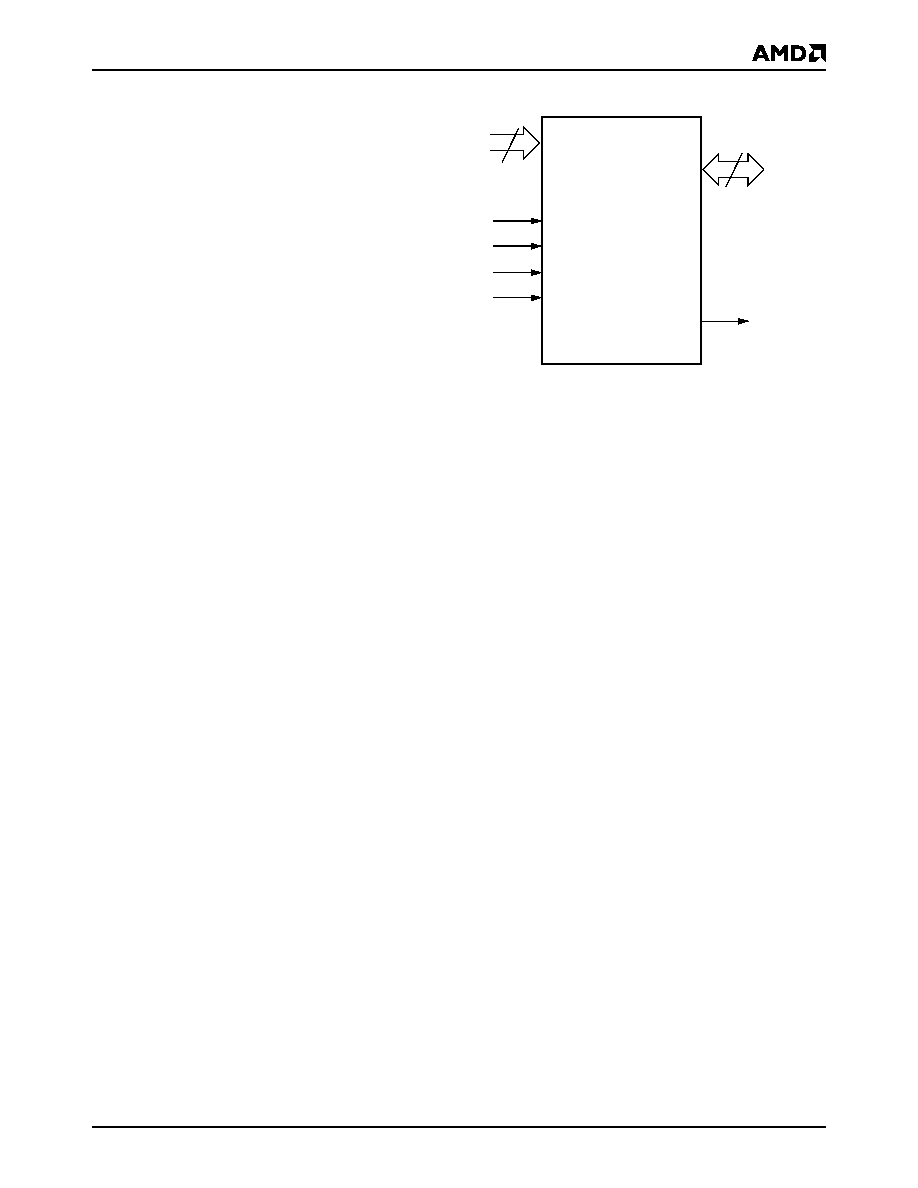
LOGIC SYMBOL
21525A-3
20
8
DQ0≠DQ7
A0≠A19
CE#
OE#
WE#
RESET#
RY/BY#