July 2003
The following document specifies Spansion memory products that are now offered by both Advanced
Micro Devices and Fujitsu. Although the document is marked with the name of the company that orig-
inally developed the specification, these products will be offered to customers of both AMD and
Fujitsu.
Continuity of Specifications
There is no change to this datasheet as a result of offering the device as a Spansion product. Any
changes that have been made are the result of normal datasheet improvement and are noted in the
document revision summary, where supported. Future routine revisions will occur when appropriate,
and changes will be noted in a revision summary.
Continuity of Ordering Part Numbers
AMD and Fujitsu continue to support existing part numbers beginning with "Am" and "MBM". To order
these products, please use only the Ordering Part Numbers listed in this document.
For More Information
Please contact your local AMD or Fujitsu sales office for additional information about Spansion
memory solutions.
Am29LV160B
Data Sheet
Publication Number 21358 Revision
G
Amendment +1 Issue
Date
February 1, 1999

This Data Sheet states AMD's current technical specifications regarding the Product described herein. This Data
Sheet may be revised by subsequent versions or modifications due to changes in technical specifications.
Publication# 21358
Rev: G Amendment/+1
Issue Date: February 1999
Am29LV160B
16 Megabit (2 M x 8-Bit/1 M x 16-Bit)
CMOS 3.0 Volt-only Boot Sector Flash Memory
DISTINCTIVE CHARACTERISTICS
s
Single power supply operation
-- Full voltage range: 2.7 to 3.6 volt read and write
operations for battery-powered applications
-- Regulated voltage range: 3.0 to 3.6 volt read and
write operations and for compatibility with high
performance 3.3 volt microprocessors
s
Manufactured on 0.32 µm process technology
s
High performance
-- Full voltage range: access times as fast as 80 ns
-- Regulated voltage range: access times as fast as
70 ns
s
Ultra low power consumption (typical values at
5 MHz)
-- 200 nA Automatic Sleep mode current
-- 200 nA standby mode current
-- 9 mA read current
-- 20 mA program/erase current
s
Flexible sector architecture
-- One 16 Kbyte, two 8 Kbyte, one 32 Kbyte, and
thirty-one 64 Kbyte sectors (byte mode)
-- One 8 Kword, two 4 Kword, one 16 Kword, and
thirty-one 32 Kword sectors (word mode)
-- Supports full chip erase
-- Sector Protection features:
A hardware method of locking a sector to prevent
any program or erase operations within that sector
Sectors can be locked in-system or via
programming equipment
Temporary Sector Unprotect feature allows code
changes in previously locked sectors
s
Unlock Bypass Program Command
-- Reduces overall programming time when issuing
multiple program command sequences
s
Top or bottom boot block configurations
available
s
Embedded Algorithms
-- Embedded Erase algorithm automatically
preprograms and erases the entire chip or any
combination of designated sectors
-- Embedded Program algorithm automatically
writes and verifies data at specified addresses
s
Minimum 1,000,000 write cycle guarantee
per sector
s
20-year data retention at 125
∞
C
-- Reliable operation for the life of the system
s
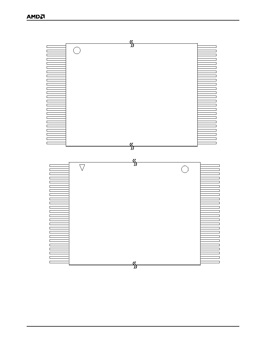
Package option
-- 48-ball FBGA
-- 48-pin TSOP
-- 44-pin SO
s
CFI (Common Flash Interface) compliant
-- Provides device-specific information to the
system, allowing host software to easily
reconfigure for different Flash devices
s
Compatibility with JEDEC standards
-- Pinout and software compatible with single-
power supply Flash
-- Superior inadvertent write protection
s
Data# Polling and toggle bits
-- Provides a software method of detecting program
or erase operation completion
s
Ready/Busy# pin (RY/BY#)
-- Provides a hardware method of detecting
program or erase cycle completion (not available
on 44-pin SO)
s
Erase Suspend/Erase Resume
-- Suspends an erase operation to read data from,
or program data to, a sector that is not being
erased, then resumes the erase operation
s
Hardware reset pin (RESET#)
-- Hardware method to reset the device to reading
array data

2
Am29LV160B
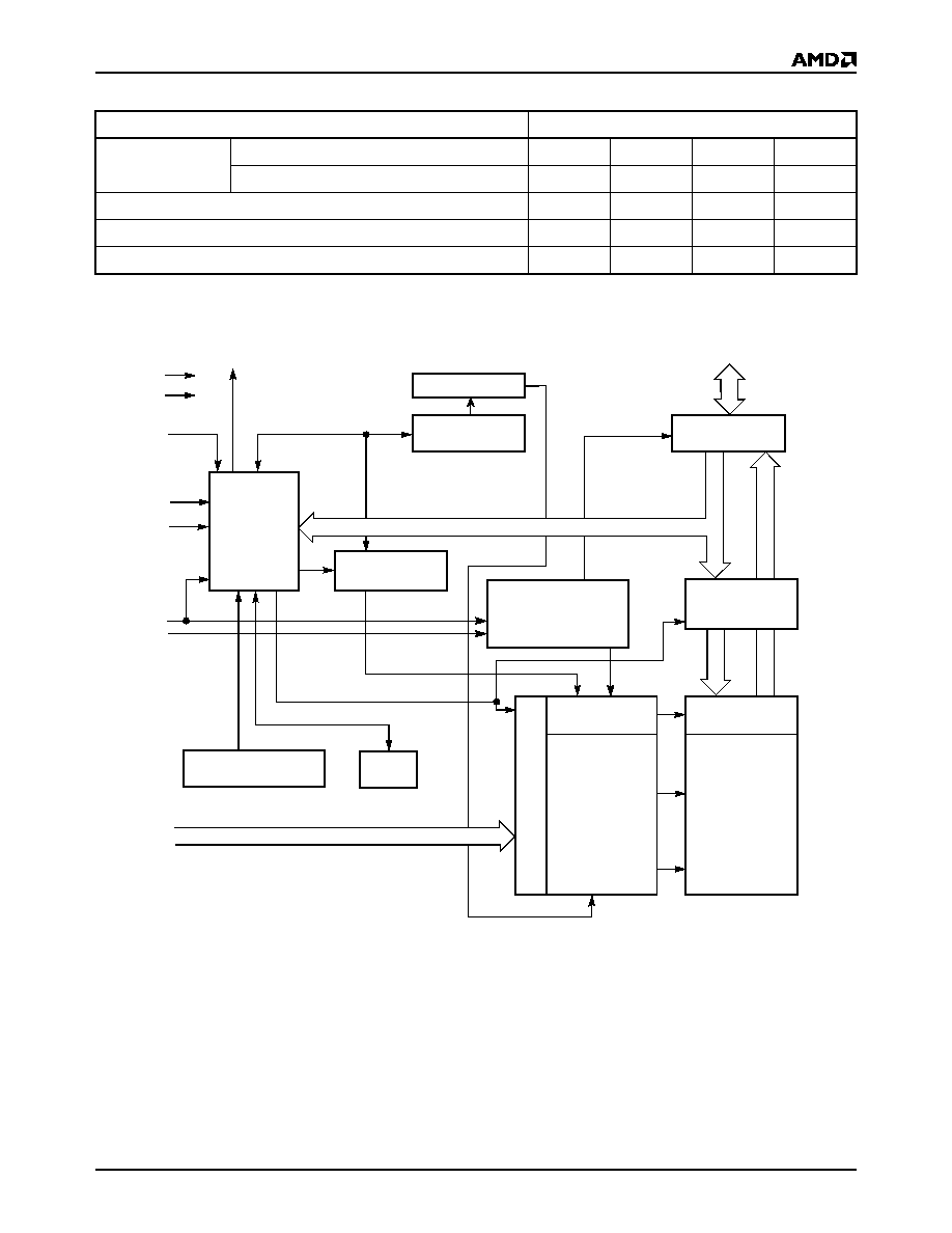
GENERAL DESCRIPTION
The Am29LV160B is a 16 Mbit, 3.0 Volt-only Flash memory
organized as 2,097,152 bytes or 1,048,576 words. The
device is offered in 48-ball FBGA, 44-pin SO, and 48-pin
TSOP packages. The word-wide data (x16) appears on
DQ15≠DQ0; the byte-wide (x8) data appears on DQ7≠DQ0.
This device is designed to be programmed in-system with
the standard system 3.0 volt V
CC
supply. A 12.0 V V
PP
or 5.0
V
CC
are not required for write or erase operations. The
d e vi ce c an a ls o b e p r og r a m m e d in s t a n da r d
EPROM programmers.
The device offers access times of 70, 80, 90, and 120 ns,
allowing high speed microprocessors to operate
without wait states. To eliminate bus contention the
device has separate chip enable (CE#), write enable
(WE#) and output enable (OE#) controls.
The device requires only a single 3.0 volt power sup-
ply for both read and write functions. Internally gener-
ated and regulated voltages are provided for the
program and erase operations.
The Am29LV160B is entirely command set compatible
with the JEDEC single-power-supply Flash stan-
dard. Commands are written to the command register
using standard microprocessor write timings. Register
contents serve as input to an internal state-machine
that controls the erase and programming circuitry.
Write cycles also internally latch addresses and data
needed for the programming and erase operations.
Reading data out of the device is similar to reading
from other Flash or EPROM devices.
Device programming occurs by executing the program
command sequence. This initiates the Embedded
Program algorithm--an internal algorithm that auto-
matically times the program pulse widths and verifies
proper cell margin. The Unlock Bypass mode facili-
tates faster programming times by requiring only two
write cycles to program data instead of four.
Device erasure occurs by executing the erase com-
mand sequence. This initiates the Embedded Erase
algorithm--an internal algorithm that automatically
preprograms the array (if it is not already programmed)
before executing the erase operation. During erase, the
device automatically times the erase pulse widths and
verifies proper cell margin.
The host system can detect whether a program or
erase operation is complete by observing the RY/BY#
pin, or by reading the DQ7 (Data# Polling) and DQ6
(toggle) status bits. After a program or erase cycle has
been completed, the device is ready to read array data
or accept another command.
The sector erase architecture allows memory sectors
to be erased and reprogrammed without affecting the
data contents of other sectors. The device is fully
erased when shipped from the factory.
Hardware data protection measures include a low V
CC
detector that automatically inhibits write operations dur-
ing power transitions. The hardware sector protection
feature disables both program and erase operations in
any combination of the sectors of memory. This can be
achieved in-system or via programming equipment.
The Erase Suspend/Erase Resume feature enables
the user to put erase on hold for any period of time to
read data from, or program data to, any sector that is
not selected for erasure. True background erase can
thus be achieved.
The hardware RESET# pin terminates any operation
in progress and resets the internal state machine to
reading array data. The RESET# pin may be tied to the
system reset circuitry. A system reset would thus also
reset the device, enabling the system microprocessor
to read the boot-up firmware from the Flash memory.
The device offers two power-saving features. When ad-
dresses have been stable for a specified amount of
time, the device enters the automatic sleep mode.
The system can also place the device into the standby
mode. Power consumption is greatly reduced in both
these modes.
AMD's Flash technology combines years of Flash
memory manufacturing experience to produce the
highest levels of quality, reliability and cost effectiveness.
The device electrically erases all bits within a sector
simultaneously via Fowler-Nordheim tunneling. The
data is programmed using hot electron injection.