FINAL
Publication# 11407
Rev: G Amendment/0
Issue Date: May 1998
Am27C2048
2 Megabit (128 K x 16-Bit) CMOS EPROM
DISTINCTIVE CHARACTERISTICS
s
Fast access time
-- Speed options as fast as 55 ns
s
Low power consumption
-- 100 µA maximum CMOS standby current
s
JEDEC-approved pinout
-- Plug-in upgrade of 1 Mbit EPROM
-- 40-pin DIP/PDIP
-- 44-pin PLCC
s
Single +5 V power supply
s
±
10% power supply tolerance standard
s
100% Flashrite programming
-- Typical programming time of 16 seconds
s
Latch-up protected to 100 mA from ≠1 V to
V
CC
+ 1 V
s
Versatile features for simple interfacing
-- Both CMOS and TTL input/output compatibility
-- Two line control functions
s
High noise immunity
GENERAL DESCRIPTION
The Am27C2048 is a 2 Mbit, ultraviolet erasable pro-
grammable read-only memory. It is organized as 128 K
words, operates from a single +5 V supply, has a static
standby mode, and features fast single address loca-
tion programming. The Am27C2048 is ideal for use in
16-bit microprocessor systems. The device is available
in windowed ceramic DIP packages, and plastic one
time programmable (OTP) PDIP and PLCC packages.
Data can be typically accessed in less than 55 ns, al-
lowing high-performance microprocessors to operate
without any WAIT states. The device offers separate
Output Enable (OE#) and Chip Enable (CE#) controls,
thus eliminating bus contention in a multiple bus micro-
processor system.
AMD's CMOS process technology provides high
speed, low power, and high noise immunity. Typical
power consumption is only 125 mW in active mode,
and 100 µW in standby mode.
All signals are TTL levels, including programming sig-
nals. Bit locations may be programmed singly, in
blocks, or at random. The device supports AMD's
Flashrite programming algorithm (100 µs pulses), re-
sulting in a typical programming time of 16 seconds.
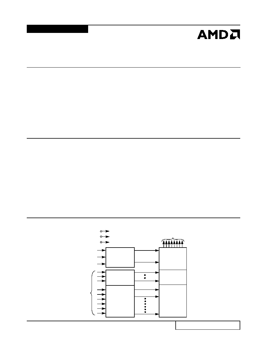
BLOCK DIAGRAM
11407G-1
A0≠A16
Address
Inputs
PGM#
CE#
OE#
V
CC
V
SS
V
PP
Data Outputs
DQ0≠DQ15
Output
Buffers
Y
Gating
2,097,152
Bit Cell
Matrix
X
Decoder
Y
Decoder
Output Enable
Chip Enable
and
Prog Logic
Am27C2048
3
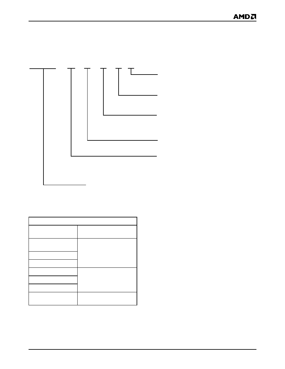
ORDERING INFORMATION
UV EPROM Products
AMD standard products are available in several packages and operating ranges. The order number (Valid Combination) is formed
by a combination of the following:
Valid Combinations
Valid Combinations list configurations planned to be sup-
ported in volume for this device. Consult the local AMD sales
office to confirm availability of specific valid combinations and
to check on newly released combinations.
DEVICE NUMBER/DESCRIPTION
Am27C2048
2 Megabit (128 K x 16-Bit) CMOS UV EPROM
AM27C2048
-55
D
C
OPTIONAL PROCESSING
Blank = Standard Processing
B
= Burn-In
VOLTAGE TOLERANCE
5
= V
CC
±
5%, 55 ns only
See Product Selector Guide and Valid Combinations
TEMPERATURE RANGE
C = Commercial (0
∞
C to +70
∞
C)
I
= Industrial (≠40
∞
C to +85
∞
C)
E
= Extended (≠55
∞
C to +125
∞
C)
PACKAGE TYPE
D = 40-Pin Ceramic DIP (CDV040)
SPEED OPTION
See Product Selector Guide and
Valid Combinations
B
5
Valid Combinations
AM27C2048-55
V
CC
= 5.0 V
±
5%
DC5, DC5B, DI5, DI5B
AM27C2048-55
V
CC
= 5.0 V
±
10%
DC, DCB, DI, DIB
AM27C2048-70
AM27C2048-90
AM27C2048-120
DC, DCB, DE, DEB, DI, DIB
AM27C2048-150
AM27C2048-200
AM27C2048-255
V
CC
= 5.0 V
±
5%
DC, DCB, DI, DIB
4
Am27C2048
ORDERING INFORMATION
OTP EPROM Products
AMD standard products are available in several packages and operating ranges. The order number (Valid Combination) is formed
by a combination of the following:
Valid Combinations
Valid Combinations list configurations planned to be sup-
ported in volume for this device. Consult the local AMD sales
office to confirm availability of specific valid combinations and
to check on newly released combinations.
DEVICE NUMBER/DESCRIPTION
Am27C2048
2 Megabit (128 K x 16-Bit) CMOS OTP EPROM
AM27C2048
-55
J
C
OPTIONAL PROCESSING
Blank = Standard Processing
VOLTAGE TOLERANCE
5
= V
CC
±
5%, -55 ns only
See Product Selector Guide and
Valid Combinations
TEMPERATURE RANGE
C = Commercial (0
∞
C to +70
∞
C)
I
= Industrial (≠40
∞
C to +85
∞
C)
PACKAGE TYPE
P
= 40-Pin Plastic DIP (PD 040)
J
= 44-Pin Square Plastic Leaded Chip Carrier (PL 044)
SPEED OPTION
See Product Selector Guide and
Valid Combinations
5
Valid Combinations
AM27C2048-55
V
CC
= 5.0 V
±
5%
PC5, PI5, JC5, JI5
AM27C2048-55
V
CC
= 5.0 V
±
10%
PC, PI, JC, JI
AM27C2048-70
AM27C2048-90
AM27C2048-120
AM27C2048-150
AM27C2048-200
AM27C2048-255
V
CC
= 5.0 V
±
5%

Am27C2048
5
FUNCTIONAL DESCRIPTION
Device Erasure
In order to clear all locations of their programmed con-
tents, the device must be exposed to an ultraviolet light
source. A dosage of 15 W seconds/cm
2
is required to
completely erase the device. This dosage can be ob-
tained by exposure to an ultraviolet lamp--wavelength
of 2537 ≈--with intensity of 12,000 µW/cm
2
for 15 to 20
minutes. The device should be directly under and about
one inch from the source, and all filters should be re-
moved from the UV light source prior to erasure.
Note that all UV erasable devices will erase with light
sources having wavelengths shorter than 4000 ≈, such
as fluorescent light and sunlight. Although the erasure
process happens over a much longer time period, ex-
posure to any light source should be prevented for
maximum system reliability. Simply cover the package
window with an opaque label or substance.
Device Programming
Upon delivery, or after each erasure, the device has
all of its bits in the "ONE", or HIGH state. "ZEROs" are
loaded into the device through the programming pro-
cedure.
The device enters the programming mode when 12.75
V
±
0.25 V is applied to the V
PP
pin, and CE# and
PGM# are at V
IL
.
For programming, the data to be programmed is ap-
plied 16 bits in parallel to the data pins.
The flowchart in the Programming section (Section 5,
Figure 5-1) shows AMD's Flashrite algorithm. The
Flashrite algorithm reduces programming time by using
a 100 µs programming pulse and by giving each address
only as many pulses to reliably program the data. After
each pulse is applied to a given address, the data in that
address is verified. If the data does not verify, additional
pulses are given until it verifies or the maximum pulses
allowed is reached. This process is repeated while se-
quencing through each address of the device. This part
of the algorithm is done at V
CC
= 6.25 V to assure that
each EPROM bit is programmed to a sufficiently high
threshold voltage. After the final address is completed,
the entire EPROM memory is verified at V
CC
= V
PP
=
5.25 V.
Please refer to Section 5 for additional programming in-
formation and specifications.
Program Inhibit
Programming different data to multiple devices in par-
allel is easily accomplished. Except for CE#, all like in-
puts of the devices may be common. A TTL low-level
program pulse applied to one device's CE# input with
V
PP
= 12.75 V
±
0.25 V and PGM# LOW will program
that particular device. A high-level CE# input inhibits
the other devices from being programmed.
Program Verify
A verification should be performed on the programmed
bits to determine that they were correctly programmed.
The verify should be performed with OE# and CE#, at
V
IL
, PGM# at V
IH
, and V
PP
between 12.5 V and 13.0 V.
Autoselect Mode
The autoselect mode provides manufacturer and de-
vice identification through identifier codes on DQ0≠
DQ7. This mode is primarily intended for programming
equipment to automatically match a device to be pro-
grammed with its corresponding programming algo-
rithm. This mode is functional in the 25
∞
C
±
5
∞
C
ambient temperature range that is required when pro-
gramming the device.
To activate this mode, the programming equipment
must force V
H
on address line A9. Two identifier bytes
may then be sequenced from the device outputs by tog-
gling address line A0 from V
IL
to V
IH
(that is, changing
the address from 00h to 01h). All other address lines
must be held at V
IL
during the autoselect mode.
Byte 0 (A0 = V
IL
) represents the manufacturer code,
and Byte 1 (A0 = V
IH
), the device identifier code. Both
codes have odd parity, with DQ7 as the parity bit.
Read Mode
To obtain data at the device outputs, Chip Enable (CE#)
and Output Enable (OE#) must be driven low. CE# con-
trols the power to the device and is typically used to se-
lect the device. OE# enables the device to output data,
independent of device selection. Addresses must be
stable for at least t
ACC
≠t
OE
.
Refer to the Switching
Waveforms section for the timing diagram.
Standby Mode
The device enters the CMOS standby mode when CE#
is at V
CC
±
0.3 V. Maximum V
CC
current is reduced to
100 µA. The device enters the TTL-standby mode
when CE# is at V
IH
. Maximum V
CC
current is reduced
to 1.0 mA. When in either standby mode, the device
places its outputs in a high-impedance state, indepen-
dent of the OE# input.
Output OR-Tieing
To accommodate multiple memory connections, a
two-line control function provides:
s
low memory power dissipation, and
s
assurance that output bus contention will not occur.
CE# should be decoded and used as the primary de-
vice-selecting function, while OE# be made a common
connection to all devices in the array and connected to
