
FINAL
Publication# 18880
Rev: C Amendment/+2
Issue Date: April 1998
Am28F512A
512 Kilobit (64 K x 8-Bit)
CMOS 12.0 Volt, Bulk Erase Flash Memory with Embedded Algorithms
DISTINCTIVE CHARACTERISTICS
s
High performance
-- 70 ns maximum access time
s
CMOS low power consumption
-- 30 mA maximum active current
-- 100 µA maximum standby current
-- No data retention power consumption
s
Compatible with JEDEC-standard byte-wide
32-Pin EPROM pinouts
-- 32-pin PDIP
-- 32-pin PLCC
-- 32-pin TSOP
s
100,000 write/erase cycles minimum
s
Write and erase voltage 12.0 V
-
5%
s
Latch-up protected to 100 mA from -1 V
to V
CC
+1 V
s
Embedded Erase Electrical Bulk Chip-Erase
-- Two seconds typical chip-erase including
pre-programming
s
Embedded
Program
-- 4 µs typical byte-program including time-out
-- One second typical chip program
s
Command register architecture for
microprocessor/microcontroller compatible
write interface
s
On-chip address and data latches
s
Advanced CMOS flash memory technology
-- Low cost single transistor memory cell
s
Embedded
algorithms for completely
self-timed write/erase operations
GENERAL DESCRIPTION
The Am28F512A is a 512 Kbit Flash memory orga-
nized as 64 Kbytes of 8 bits each. AMD's Flash memo-
ries offer the most cost-effective and reliable read/write
non- volatile random access memory. The Am28F512A
is packaged in 32-pin PDIP, PLCC, and TSOP versions.
It is designed to be reprogrammed and erased in-sys-
tem or in sta ndard EPROM programmers. Th e
Am28F512A is erased when shipped from the factory.
The standard Am28F512A offers access times as fast
as 70 ns, allowing operation of high-speed micropro-
cessors without wait states. To eliminate bus conten-
tion, the Am28F512A has separate chip enable (CE#)
and output enable (OE#) controls.
AMD's Flash memories augment EPROM functionality
with in-circuit electrical erasure and programming. The
Am28F512A uses a command register to manage this
functionality, while maintaining a JEDEC Flash stan-
dard 32-pin pinout. The command register allows for
100% TTL level control inputs and fixed power supply
levels during erase and programming.
AMD's Flash technology reliably stores memory con-
tents even after 100,000 erase and program cycles.
The AMD cell is designed to optimize the erase and
programming mechanisms. In addition, the combina-
tion of advanced tunnel oxide processing and low inter-
n a l e l e c tr i c f i e l d s fo r e r a se a n d p r o gr a m m i n g
operations produces reliable cycling. The Am28F512A
uses a 12.0 V
±
5% V
PP
high voltage input to perform
the erase
and programming functions.
The highest degree of latch-up protection is achieved
with AMD's proprietary non-epi process. Latch-up pro-
tection is provided for stresses up to 100 milliamps on
address and data pins from ≠1 V to V
CC
+1 V.
Embedded Program
The Am28F512A is byte programmable using the Em-
bedded Programming algorithm. The Embedded Pro-
gramming algorithm does not require the system to
time-out or verify the data programmed. The typical
r o o m t e m p e r a t u r e p r o g r a m m i n g t i m e o f t h e
Am28F512A is one second.
Embedded Erase
The entire chip is bulk erased using the Embedded
Erase algorithm. The Embedded
Erase algorithm auto-
matically programs the entire array prior to electrical
erase. The timing and verification of electrical erase are

2
Am28F512A
controlled internal to the device. Typical erasure at room
temperature is accomplished in two seconds, including
programming.
AMD's Am28F512A is entirely pin and software com-
patible with AMD Am28F020A, Am28F010A, and
Am28F256A Flash memories.
Commands are written to the command register using
standard microprocessor write timings. Register con-
tents serve as inputs to an internal state-machine
which controls the erase and programming circuitry.
During write cycles, the command register internally
latches address and data needed for the program-
ming and erase operations. For system design simpli-
fication, the Am28F512A is designed to support either
WE# or CE controlled writes. During a system write
cycle, addresses are latched on the falling edge of
WE# or CE# whichever occurs last. Data is latched on
the rising edge of WE# or CE# whichever occurs first.
To simplify the following discussion, the WE# pin is
used as the write cycle control pin throughout the rest
of this text. All setup and hold times are with respect
to the WE# signal.
AMD's Flash technology combines years of EPROM
and EEPROM experience to produce the highest lev-
els of quality, reliability, and cost effectiveness. The
Am28F512A electrically erases all bits simulta-
neously using Fowler-Nordheim tunneling. The bytes
are programmed one byte at a time using the EPROM
programming mechanism of hot electron injection.
Comparing Embedded Algorithms with Flasherase and Flashrite Algorithms
Am28F512A with
Embedded Algorithms
Am28F512 using AMD Flashrite
and Flasherase Algorithms
Embedded
Programming
Algorithm vs.
Flashrite
Programming
Algorithm
AMD's Embedded Programming algorithm
requires the user to only write a program
set-up command and a program command
(program data and address). The device
automatically times the programming
pulse width, verifies the programming, and
counts the number of sequences. A status
bit, Data
#
Polling, provides the user with
the programming operation status.
The Flashrite Programming algorithm requires the
user to write a program set-up command, a program
command, (program data and address), and a
program verify command, followed by a read and
compare operation. The user is required to time the
programming pulse width in order to issue the
program verify command. An integrated stop timer
prevents any possibility of overprogramming.
Upon completion of this sequence, the data is read
back from the device and compared by the user with
the data intended to be written; if there is not a
match, the sequence is repeated until there is a
match or the sequence has been repeated 25 times.
Embedded Erase
Algorithm vs.
Flasherase Erase
Algorithm
AMD's Embedded Erase algorithm
requires the user to only write an erase set-
up command and erase command. The
device automatically pre-programs and
verifies the entire array. The device then
automatically times the erase pulse width,
verifies the erase operation, and counts
the number of sequences. A status bit,
Data
#
Polling, provides the user with the
erase operation status.
The Flasherase Erase algorithm requires the device
to be completely programmed prior to executing an
erase command.
To invoke the erase operation, the user writes an
erase set-up command, an erase command, and an
erase verify command. The user is required to time
the erase pulse width in order to issue the erase
verify command. An integrated stop timer prevents
any possibility of overerasure.
Upon completion of this sequence, the data is read
back from the device and compared by the user with
erased data. If there is not a match, the sequence is
repeated until there is a match or the sequence has
been repeated 1,000 times.
Am28F512A
3
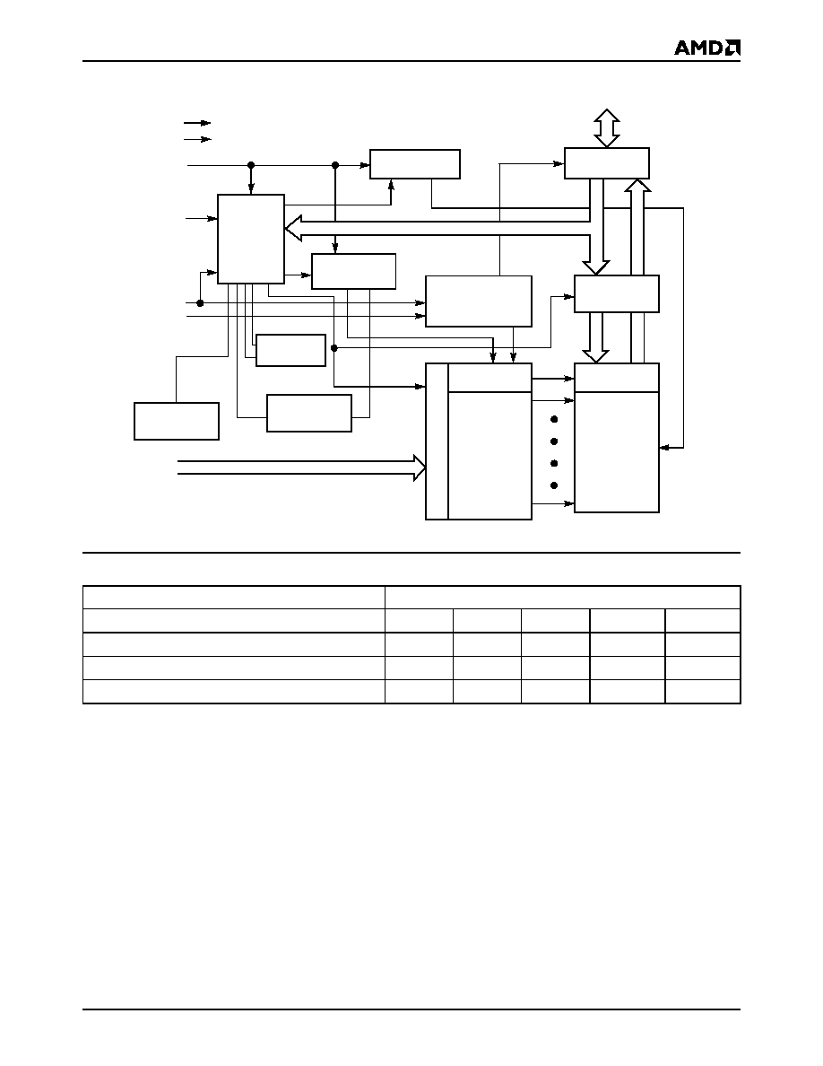
BLOCK DIAGRAM
PRODUCT SELECTOR GUIDE
Family Part Number
Am28F512A
Speed Options (V
CC
= 5.0 V
±
10%)
-70
-90
-120
-150
-200
Max Access Time (ns)
70
90
120
150
200
CE
#
(E
#
) Access (ns)
70
90
120
150
200
OE
#
(G
#
) Access (ns)
35
35
50
55
55
Erase Voltage
Switch
Input/Output
Buffers
Data
Latch
Y-Gating
524,288
Bit Cell Matrix
X-Decoder
Y-Decoder
Ad
dre
ss L
atc
h
Chip Enable
Output Enable
Logic
Program
Voltage Switch
State
Control
Command
Register
WE
#
CE
#
OE#
A0≠A15
DQ0≠DQ7
V
CC
V
SS
18880C-1
Low V
CC
Detector
Program/Erase
Pulse Timer
V
PP
To Array
Embedded
Algorithms
4
Am28F512A
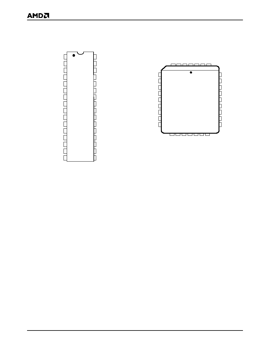
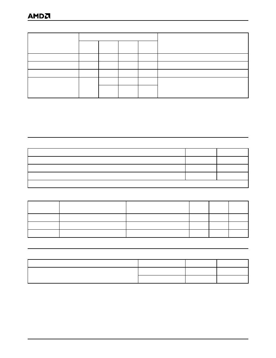
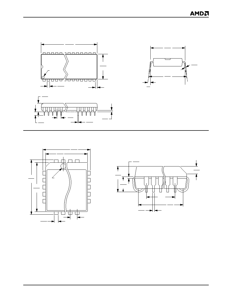
CONNECTION DIAGRAMS
Note: Pin 1 is marked for orientation.
3
4
5
2
1
9
10
11
12
13
27
26
25
24
23
7
8
22
21
6
32
31
20
14
30
29
28
15
16
19
18
17
A6
A5
A4
A3
A2
A1
A0
NC
DQ0
A15
A12
A7
DQ1
DQ2
VSS
A8
A9
A11
OE# (G#)
A10
CE# (E#)
DQ7
VCC
WE# (W#)
DQ6
NC
A14
A13
DQ5
DQ4
DQ3
VPP
18880C-2
PDIP
1
31 30
2
3
4
5
6
7
8
9
10
11
12
13
17 18 19 20
16
15
14
29
28
27
26
25
24
23
22
21
32
A
7
A
6
A
5
A
4
A
3
A
2
A
1
A
0
DQ
0
A
14
A
13
A
8
A
9
A
11
OE# (G#)
A
10
CE (E#)
DQ
7
A
12
A
15
NC
V
PP
V
CC
WE# (W#)
NC
DQ
1
DQ
2
V
SS
DQ
3
DQ
4
DQ
5
DQ
6
PLCC
18880C-3
Am28F512A
5
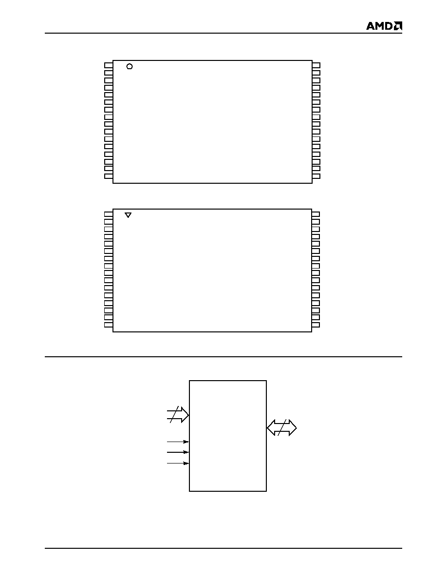
CONNECTION DIAGRAMS (Continued)
LOGIC SYMBOL
1
2
3
4
5
6
7
8
9
10
11
12
13
14
15
16
32-Pin TSOP--Standard Pinout
A11
A9
A8
A13
A14
NC
WE
#
V
CC
V
PP
NC
A15
A12
A7
A6
A5
A4
32
31
30
29
28
27
26
25
24
23
22
21
20
19
18
17
OE
#
A10
CE
#
D7
D6
D5
D4
D3
V
SS
D2
D1
D0
A0
A1
A2
A3
32-Pin TSOP--Reverse Pinout
1
2
3
4
5
6
7
8
9
10
11
12
13
14
15
16
A11
A9
A8
A13
A14
NC
WE
#
V
CC
V
PP
NC
A15
A12
A7
A6
A5
A4
32
31
30
29
28
27
26
25
24
23
22
21
20
19
18
17
OE
#
A10
CE
#
D7
D6
D5
D4
D3
V
SS
D2
D1
D0
A0
A1
A2
A3
18880C-4
16
8
DQ0≠DQ7
A0≠A15
CE
#
(E
#
)
OE
#
(G#)
WE
#
(W
#
)
18880C-5
6
Am28F512A
ORDERING INFORMATION
Standard Products
AMD standard products are available in several packages and operating ranges. The order number (Valid Combination) is formed
by a combination of:
Valid Combinations
Valid Combinations list configurations planned to be sup-
ported in volume for this device. Consult the local AMD sales
office to confirm availability of specific valid combinations and
to check on newly released combinations.
DEVICE NUMBER/DESCRIPTION
Am28F512A
512 Kilobit (64 K x 8-Bit) 12.0 Volt CMOS Flash Memory with Embedded Algorithms
AM28F512A -70
J
C
OPTIONAL PROCESSING
Blank = Standard Processing
B
= Burn-In
Contact an AMD representative for more information.
TEMPERATURE RANGE
C = Commercial (0∞C to +70∞C)
I = Industrial (≠40∞C to +85∞C)
E = Extended (≠55∞C to +125∞C)
PACKAGE TYPE
P = 32-Pin Plastic DIP (PD 032)
J = 32-Pin Rectangular Plastic Leaded Chip
Carrier (PL 032)
E = 32-Pin Thin Small Outline Package (TSOP)
Standard Pinout (TS 032)
F = 32-Pin Thin Small Outline Package (TSOP)
Reverse Pinout (TSR032)
SPEED OPTION
See Product Selector Guide and Valid Combinations
B
Valid Combinations
AM28F512A-70
PC, PI, PE,
JC, JI, JE,
EC, EI, EE,
FC, FI, FE
AM28F512A-90
AM28F512A-120
AM28F512A-150
AM28F512A-200

Am28F512A
7
PIN DESCRIPTION
A0≠A15
A
ddress Inputs for memory locations. Internal latches
hold addresses during write cycles.
CE
#
(E
#
)
Chip Enable active low input activates the chip's con-
trol logic and input buffers. Chip Enable high will dese-
lect the device and operates the chip in stand-by mode.
DQ0≠DQ7
Data Inputs during memory write cycles. Internal
latches hold data during write cycles. Data Outputs
during memory read cycles.
NC
No Connect-corresponding pin is not connected
internally to the die.
OE
#
(G
#
)
Output Enable active low input gates the outputs of the
device through the data buffers during memory read
cycles. Output Enable is high during command
sequencing and program/erase operations.
V
CC
Power supply for device operation. (5.0 V
±
5% or 10%)
V
PP
Program voltage input. V
PP
must be at high voltage in
order to write to the command register. The command
register controls all functions required to alter the mem-
ory array contents. Memory contents cannot be altered
when V
PP
V
CC
+2 V.
V
SS
Ground.
WE
#
(W
#
)
Write Enable active low input controls the write function
of the command register to the memory array. The tar-
get address is latched on the falling edge of the Write
Enable pulse and the appropriate data is latched on the
rising edge of the pulse. Write Enable high inhibits
writing to the device.

8
Am28F512A
BASIC PRINCIPLES
This section contains descriptions about the device
read, erase, and program operations, and write opera-
tion status of the Am29FxxxA, 12.0 volt family of Flash
devices. References to some tables or figures may be
given in generic form, such as "Command Definitions
table", rather than "Table 1". Refer to the corresponding
data sheet for the actual table or figure.
The Am28FxxxA family uses 100% TTL-level control
inputs to manage the command register. Erase and
reprogramming operations use a fixed 12.0 V
±
5%
high voltage input.
Read Only Memory
Without high V
PP
voltage, the device functions as a
read only memory and operates like a standard
EPROM. The control inputs still manage traditional
read, standby, output disable, and Auto select modes.
Command Register
The command register is enabled only when high volt-
age is applied to the V
PP
pin. The erase and repro-
gramming operations are only accessed via the
register. In addition, two-cycle commands are required
for erase and reprogramming operations. The tradi-
tional read, standby, output disable, and Auto select
modes are available via the register.
The device's command register is written using standard
microprocessor write timings. The register controls an
internal state machine that manages all device opera-
tions. For system design simplification, the device is de-
signed to support either WE# or CE# controlled writes.
During a system write cycle, addresses are latched on
the falling edge of WE# or CE# whichever occurs last.
Data is latched on the rising edge of WE# or CE# which-
ever occur first. To simplify the following discussion, the
WE# pin is used as the write cycle control pin throughout
the rest of this text. All setup and hold times are with re-
spect to the WE# signal.
OVERVIEW OF ERASE/PROGRAM
OPERATIONS
Embedded
Erase Algorithm
AMD now makes erasure extremely simple and reli-
able. The Embedded Erase algorithm requires the user
to only write an erase setup command and erase com-
mand. The device will automatically pre-program and
verify the entire array. The device automatically times
the erase pulse width, provides the erase verify and
counts the number of sequences. A status bit, Data#
Polling, provides feedback to the user as to the status
of the erase operation.
Embedded Programming Algorithm
AMD now makes programming extremely simple and
reliable. The Embedded Programming algorithm re-
quires the user to only write a program setup command
and a program command. The device automatically
times the programming pulse width, provides the pro-
gram verify and counts the number of sequences. A
status bit, Data# Polling, provides feedback to the user
as to the status of the programming operation.
DATA PROTECTION
The device is designed to offer protection against acci-
dental erasure or programming caused by spurious
system level signals that may exist during power transi-
tions. The device powers up in its read only state. Also,
with its control register architecture, alteration of the
memory contents only occurs after successful comple-
tion of specific command sequences.
The device also incorporates several features to pre-
vent inadvertent write cycles resulting from V
CC
power-up and power-down transitions or system noise.
Low V
CC
Write Inhibit
To avoid initiation of a write cycle during V
CC
power-up
and power-down, the device locks out write cycles for
V
CC
< V
LKO
(see DC characteristics section for volt-
ages). When V
CC
< V
LKO
, the command register is dis-
abled, all internal program/erase circuits are disabled,
and the device resets to the read mode. The device ig-
nores all writes until V
CC
> V
LKO
. The user must ensure
that the control pins are in the correct logic state when
V
CC
> V
LKO
to prevent unintentional writes.
Write Pulse "Glitch" Protection
Noise pulses of less than 10 ns (typical) on OE#, CE#
or WE# will not initiate a write cycle.
Logical Inhibit
Writing is inhibited by holding any one of OE# = V
IL
,
CE# =V
IH
or WE# = V
IH
. To initiate a write cycle CE#
and WE# must be a logical zero while OE# is a logical
one.
Power-Up Write Inhibit
Power-up of the device with WE# = CE# = V
IL
and
OE# = V
IH
will not accept commands on the rising
edge of WE#. The internal state machine is automati-
cally reset to the read mode on power-up.
Am28F512A
9
FUNCTIONAL DESCRIPTION
Description Of User Modes
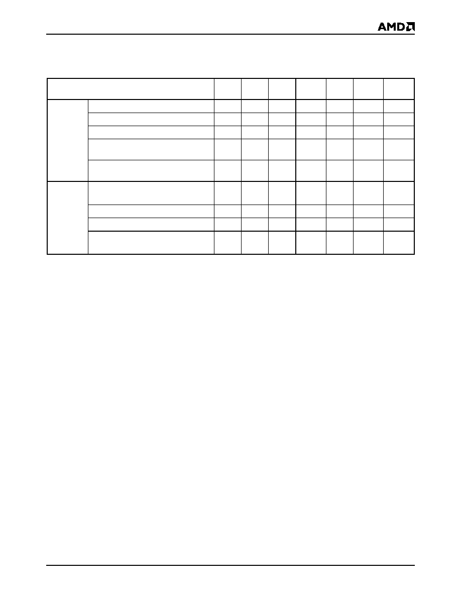
Table 1.
Am28F512A Device Bus Operations (Notes 7 and 8)
Legend:
X = Don't care, where Don't Care is either V
IL
or V
IH
levels. V
PPL
= V
PP
<
V
CC
+ 2 V. See DC Characteristics for voltage levels
of V
PPH
. 0 V < An < V
CC
+ 2 V, (normal TTL or CMOS input levels, where n = 0 or 9).
Notes:
1. V
PPL
may be grounded, connected with a resistor to ground, or < V
CC
+ 2.0 V. V
PPH
is the programming voltage specified for
the device. Refer to the DC characteristics. When V
PP
= V
PPL
, memory contents can be read but not written or erased.
2. Manufacturer and device codes may also be accessed via a command register write sequence. Refer to Table 2.
3. 11.5 < V
ID
< 13.0 V. Minimum V
ID
rise time and fall time (between 0 and V
ID
voltages) is 500 ns.
4. Read operation with V
PP
= V
PPH
may access array data or the Auto select codes.
5. With V
PP
at high voltage, the standby current is I
CC
+ I
PP
(standby).
6. Refer to Table 3 for valid D
IN
during a write operation.
7. All inputs are Don't Care unless otherwise stated, where Don't Care is either V
IL
or V
IH
levels. In the Auto select mode all
addresses except A
9
and A
0
must be held at V
IL
.
8. If V
CC
1.0 Volt, the voltage difference between V
PP
and V
CC
should not exceed 10.0 volts. Also, the Am28F256 has a V
PP
rise time and fall time specification of 500 ns minimum.
Operation
CE#
(E#)
OE#
(G#)
WE#
(W#)
V
PP
(Note 1)
A0
A9
I/O
Read-Only
Read
V
IL
V
IL
X
V
PPL
A0
A9
D
OUT
Standby
V
IH
X
X
V
PPL
X
X
HIGH Z
Output Disable
V
IL
V
IH
V
IH
V
PPL
X
X
HIGH Z
Auto-select Manufacturer
Code (Note 2)
V
IL
V
IL
V
IH
V
PPL
V
IL
V
ID
(Note 3)
CODE
(01h)
Auto-select Device
Code (Note 2)
V
IL
V
IL
V
IH
V
PPL
V
IH
V
ID
(Note 3)
CODE
(AEh)
Read/Write
Read
V
IL
V
IL
V
IH
V
PPH
A0
A9
D
OUT
(Note 4)
Standby (Note 5)
V
IH
X
X
V
PPH
X
X
HIGH Z
Output Disable
V
IL
V
IH
V
IH
V
PPH
X
X
HIGH Z
Write
V
IL
V
IH
V
IL
V
PPH
A0
A9
D
IN
(Note 6)
10
Am28F512A
READ-ONLY MODE
When V
PP
is less than V
CC
+ 2 V, the command register
is inactive. The device can either read array or autose-
lect data, or be standby mode.
Read
The device functions as a read only memory when V
PP
< V
CC
+ 2 V.
The device has two control functions. Both
must be satisfied in order to output data. CE# controls
power to the device. This pin should be used for spe-
cific device selection. OE# controls the device outputs
and should be used to gate data to the output pins if a
device is selected.
Address access time t
ACC
is equal to the delay from
stable addresses to valid output data. The chip enable
access time t
CE
is the delay from stable addresses and
stable CE# to valid data at the output pins. The output
enable access time is the delay from the falling edge of
OE# to valid data at the output pins (assuming the ad-
dresses have been stable at least t
ACC
- t
OE
).
Standby Mode
The device has two standby modes. The CMOS
standby mode (CE# input held at V
CC
±
0.5 V), con-
sumes less than 100 µA of current. TTL standby mode
(CE# is held at V
IH
) reduces the current requirements
to less than 1 mA. When in the standby mode the out-
puts are in a high impedance state, independent of the
OE# input.
If the device is deselected during erasure, program-
ming, or program/erase verification, the device will
draw active current until the operation is terminated.
Output Disable
Output from the device is disabled when OE# is at a
logic high level. When disabled, output pins are in a
high impedance state.
Auto Select
Flash memories can be programmed in-system or in a
standard PROM programmer. The device may be sol-
dered to the circuit board upon receipt of shipment and
programmed in-system. Alternatively, the device may
initially be programmed in a PROM programmer prior
to soldering the device to the board.
The Auto select mode allows the reading out of a binary
code from the device that will identify its manufacturer and
type. This mode is intended for the purpose of automati-
cally matching the device to be programmed with its cor-
responding programming algorithm. This mode is
functional over the entire temperature range of the device.
Programming In A PROM Programmer
To activate this mode, the programming equipment
must force V
ID
(11.5 V to 13.0 V) on address A9. Two
identifier bytes may then be sequenced from the device
outputs by toggling address A0 from V
IL
to V
IH
. All other
address lines must be held at V
IL
, and V
PP
must
be
less than or equal to V
CC
+ 2.0 V while using this Auto
select mode. Byte 0 (A0 = V
IL
) represents the manufac-
turer code and byte 1 (A0 = V
IH
) the device identifier
code. For the device the two bytes are given in the table
2 of the device data sheet. All identifiers for manufac-
turer and device codes will exhibit odd parity with the
MSB (DQ7) defined as the parity bit.
Table 2.
Am28F512A Auto Select Code
Type
A0
Code
(HEX)
Manufacturer Code
V
IL
01
Device Code
V
IH
AE
Am28F512A
11
ERASE, PROGRAM, AND READ MODE
When V
PP
is equal to 12.0 V ± 5%, the command reg-
ister is active. All functions are available. That is, the
device can program, erase, read array or autoselect
data, or be standby mode.
Write Operations
High voltage must be applied to the V
PP
pin in order to
activate the command register. Data written to the reg-
ister serves as input to the internal state machine. The
output of the state machine determines the operational
function of the device.
The command register does not occupy an address-
able memory location. The register is a latch that stores
the command, along with the address and data infor-
mation needed to execute the command. The register
is written by bringing WE# and CE# to V
IL
, while OE#
is at V
IH
. Addresses are latched on the falling edge of
WE#, while data is latched on the rising edge of the
WE# pulse. Standard microprocessor write timings are
used.
The device requires the OE# pin to be V
IH
for write op-
erations. This condition eliminates the possibility for
bus contention during programming operations. In
order to write, OE# must be V
IH
, and CE# and WE#
must be V
IL
. If any pin is not in the correct state a write
command will not be executed.
Refer to AC Write Characteristics and the Erase/Pro-
gramming Waveforms for specific timing parameters.
Command Definitions
The contents of the command register default to 00h
(Read Mode) in the absence of high voltage applied to
the V
PP
pin. The device operates as a read only
memory. High voltage on the V
PP
pin enables the
command register. Device operations are selected by
writing specific data codes into the command register.
Table 3 in the device data sheet defines these register
commands.
Read Command
Memory contents can be accessed via the read com-
mand when V
PP
is high. To read from the device, write
00h into the command register. Standard microproces-
sor read cycles access data from the memory. The de-
vice will remain in the read mode until the command
register contents are altered.
The command register defaults to 00h (read mode)
upon V
PP
power-up. The 00h (Read Mode) register de-
fault helps ensure that inadvertent alteration of the
memory contents does not occur during the V
PP
power
transition. Refer to the AC Read Characteristics and
Waveforms for the specific timing parameters.
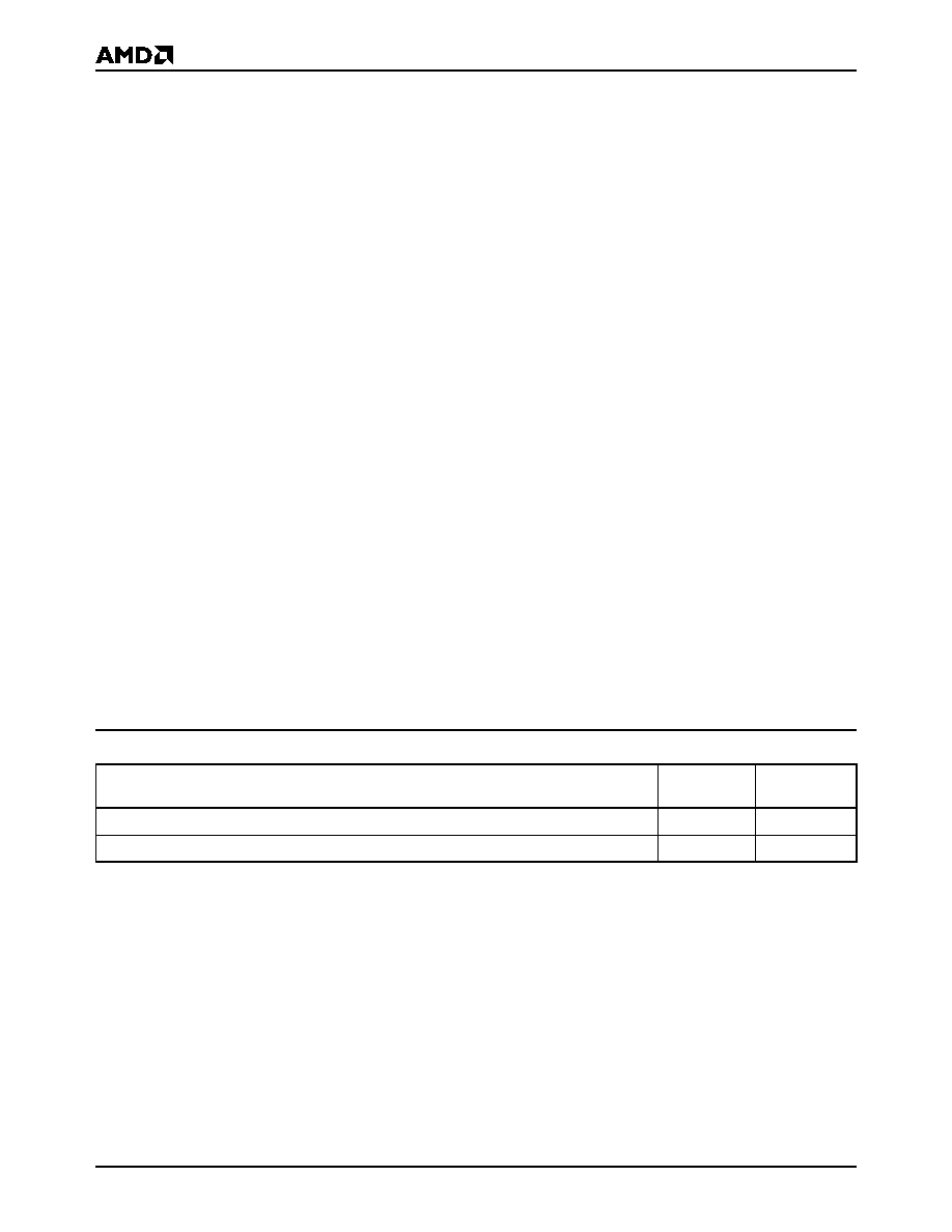
Table 3.
Am28F512A Command Definitions
Notes:
1. Bus operations are defined in Table 1.
2. RA = Address of the memory location to be read.
PA = Address of the memory location to be programmed.
Addresses are latched on the falling edge of the WE
#
pulse.
X = Don't care.
3. RD = Data read from location RA during read operation.
PD = Data to be programmed at location PA. Data latched on the rising edge of WE
#
.
4. Please reference Reset Command section.
Command
First Bus Cycle
Second Bus Cycle
Operation
(Note 1)
Address
(Note 2)
Data
(Note 3)
Operation
(Note 1)
Address
(Note 2)
Data
(Note 3)
Read Memory (Note 4)
Write
X
00h/FFh
Read
RA
RD
Read Auto select
Write
X
80h or 90h
Read
00h/01h
01h/AEh
Embedded Erase Set-up/
Embedded Erase
Write
X
30h
Write
X
30h
Embedded Program Set-up/
Embedded Program
Write
X
10h or 50h
Write
PA
PD
Reset (Note 4)
Write
X
00h/FFh
Write
X
00h/FFh
12
Am28F512A
FLASH MEMORY PROGRAM/ERASE
OPERATIONS
Embedded Erase Algorithm
The automatic chip erase does not require the device
to be entirely pre-programmed prior to executing the
Embedded set-up erase command and Embedded
erase command. Upon executing the Embedded erase
command the device automatically will program and
verify the entire memory for an all zero data pattern.
The system is
not required to provide any controls or
timing during these operations.
When the device is automatically verified to contain an
all zero pattern, a self-timed chip erase and verify be-
gin. The erase and verify operation are complete when
the data on DQ7 is "1" (see Write Operation Status sec-
tion) at which time the device returns to Read mode.
The system is not required to provide any control or
timing during these operations.
When using the Embedded Erase algorithm, the erase
automatically terminates when adequate erase margin
has been achieved for the memory array (no erase ver-
ify command is required). The margin voltages are in-
ternally generated in the same manner as when the
standard erase verify command is used.
The Embedded Erase Set-Up command is a command
only operation that stages the device for automatic
electrical erasure of all bytes in the array. Embedded
Erase Setup is performed by writing 30h to the com-
mand register.
To commence automatic chip erase, the command 30h
must be written again to the command register. The au-
tomatic erase begins on the rising edge of the WE and
terminates when the data on DQ7 is "1" (see Write Op-
eration Status section) at which time the device returns
to Read mode.
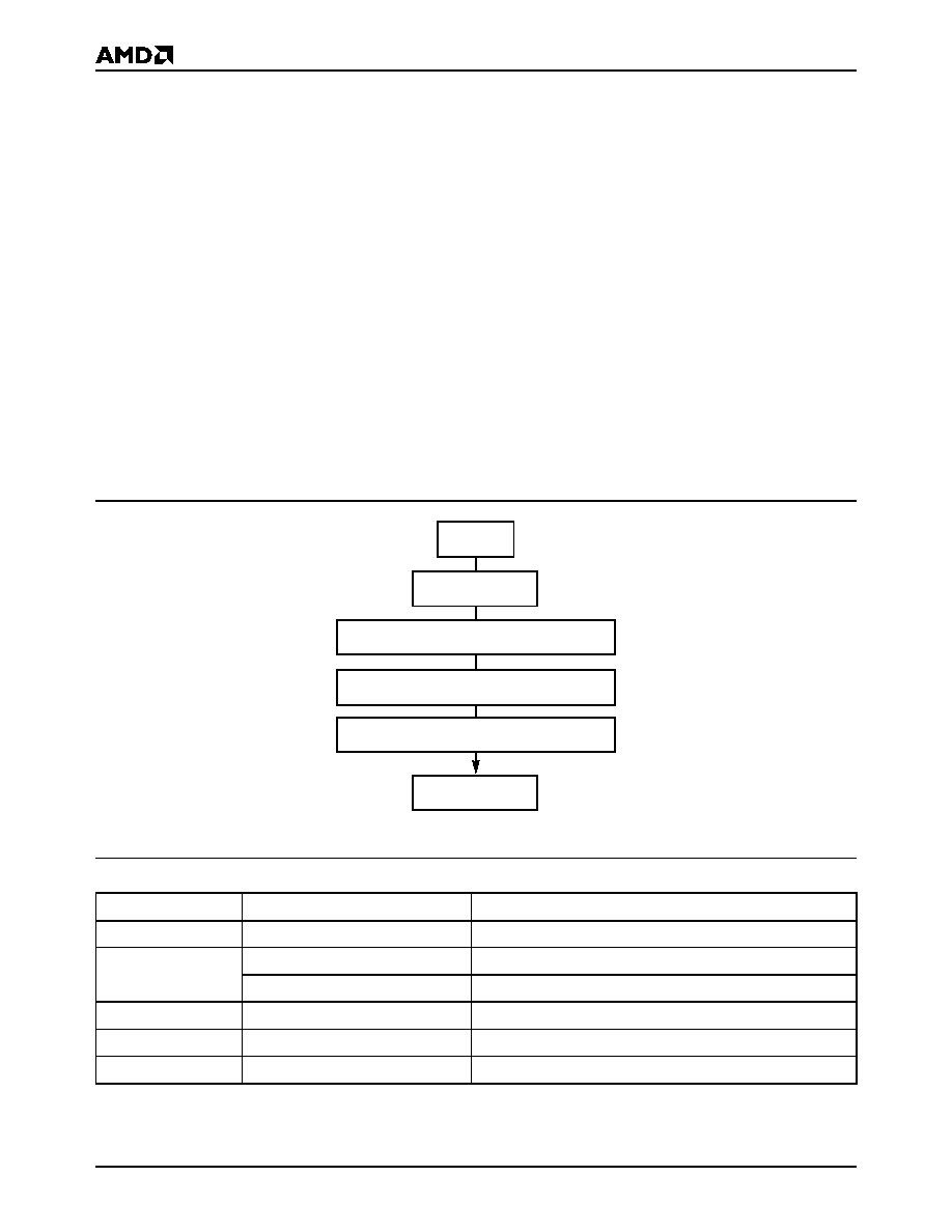
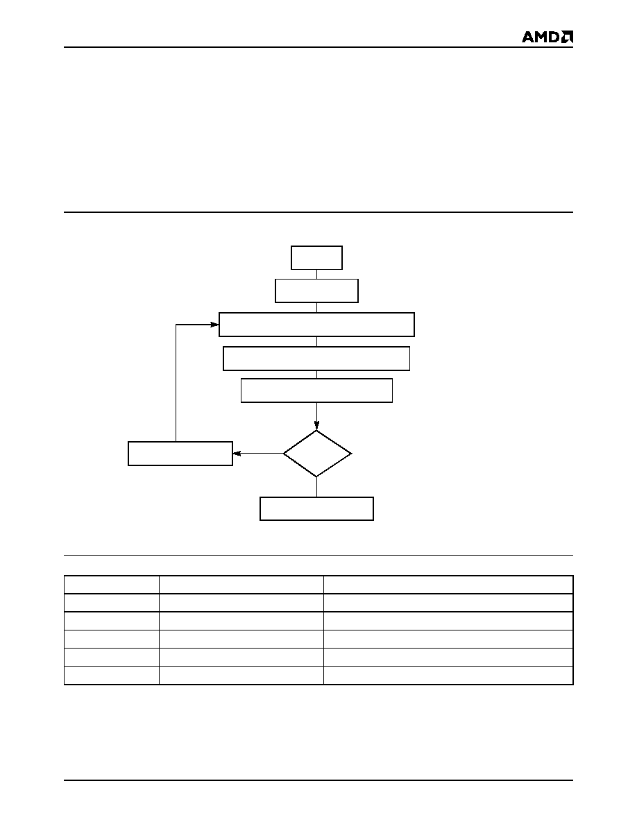
Figure 1 and Table 4 illustrate the Embedded Erase al-
gorithm, a typical command string and bus operation.
Table 4.
Embedded Erase Algorithm
Note: See AC and DC Characteristics for values of V
PP
parameters. The V
PP
power supply can be hard-wired to the device or
switchable. When V
PP
is switched, V
PPL
may be ground, no connect with a resistor tied to ground, or less than V
CC
+ 2.0 V. Refer
to Functional Description.
Bus Operations
Command
Comments
Standby
Wait for V
PP
Ramp to V
PPH
(see Note)
Write
Embedded Erase Setup Command
Data = 30h
Embedded Erase Command
Data = 30h
Read
Data
#
Polling to Verify Erasure
Standby
Compare Output to FFh
Read
Available for Read Operations
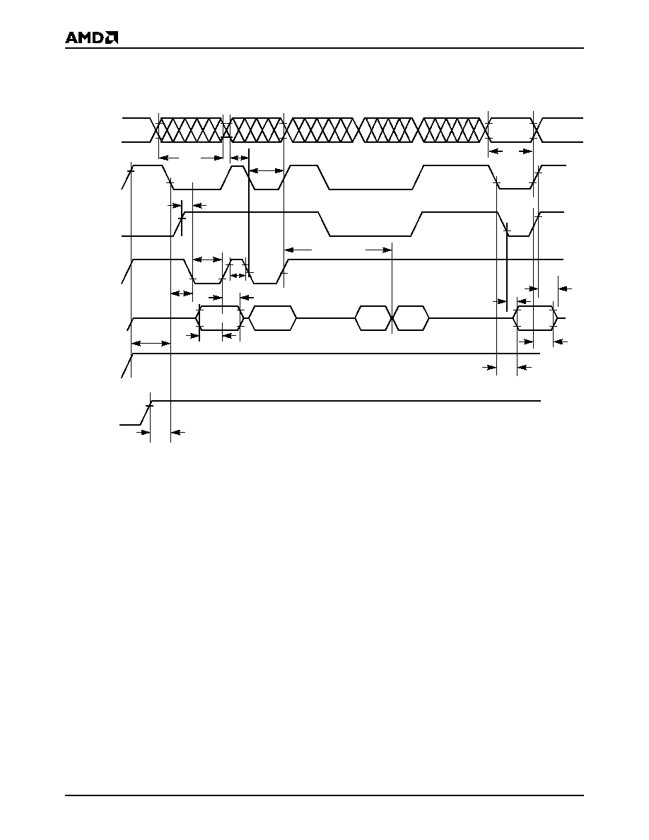
START
Apply V
PPH
Erasure Completed
Data# Poll from Device
Write Embedded Erase Command
Write Embedded Erase Setup Command
18880C-6
Figure 1.
Embedded Erase Algorithm
Am28F512A
13
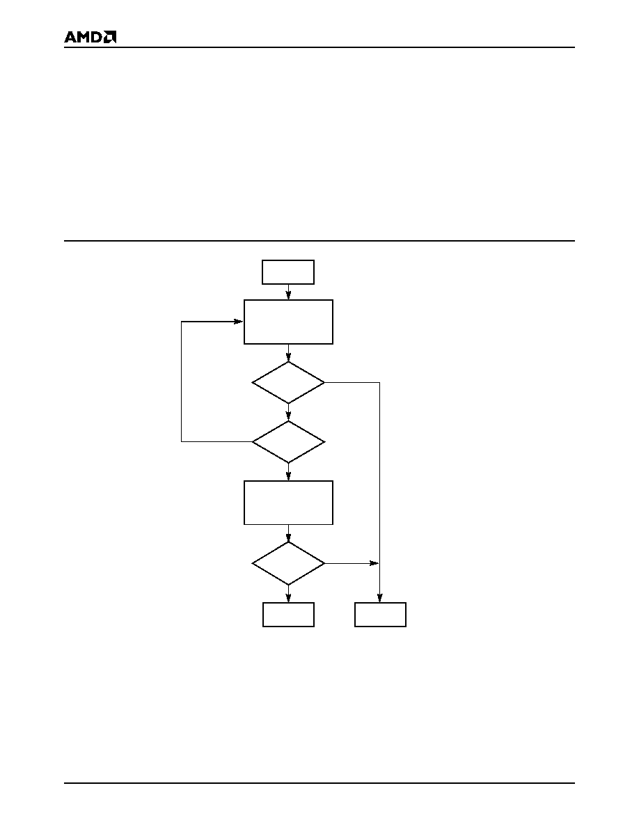
Embedded Programming Algorithm
The Embedded Program Setup is a command only op-
eration that stages the device for automatic program-
ming. Embedded Program Setup is performed by
writing 10h or 50h to the command register.
Once the Embedded Setup Program operation is per-
formed, the next WE# pulse causes a transition to an
active programming operation. Addresses are latched
on the falling edge of CE# or WE# pulse, whichever
happens later. Data is latched on the rising edge of
WE# or CE#, whichever happens first. The rising edge
of WE# also begins the programming operation. The
system is not required to provide further controls or
timings. The device will automatically provide an ade-
quate internally generated program pulse and verify
margin. The automatic programming operation is
completed when the data on DQ7 is equivalent to data
written to this bit (see Write Operation Status section)
at which time the device returns to Read mode.
Figure 2 and Table 5 illustrate the Embedded Program
algorithm, a typical command string, and bus operation.
Table 5.
Embedded Programming Algorithm
Note: See AC and DC Characteristics for values of V
PP
parameters. The V
PP
power supply can be hard-wired to the device or
switchable. When V
PP
is switched, V
PPL
may be ground, no connect with a resistor tied to ground, or less than V
CC
+ 2.0 V. Refer
to Functional Description. Device is either powered-down, erase inhibit or program inhibit.
Bus Operations
Command
Comments
Standby
Wait for V
PP
Ramp to V
PPH
(see Note)
Write
Embedded Program Setup Command
Data = 10h or 50h
Write
Embedded Program Command
Valid Address/Data
Read
Data
#
Polling to Verify Completion
Read
Available for Read Operations
START
Apply V
PPH
Write Embedded Setup Program Command
Write Embedded
Program Command (A/D)
Programming Completed
Yes
Data# Poll Device
Increment Address
No
18880C-7
Figure 2.
Embedded Programming Algorithm
Last Address
14
Am28F512A
Write Operation Status
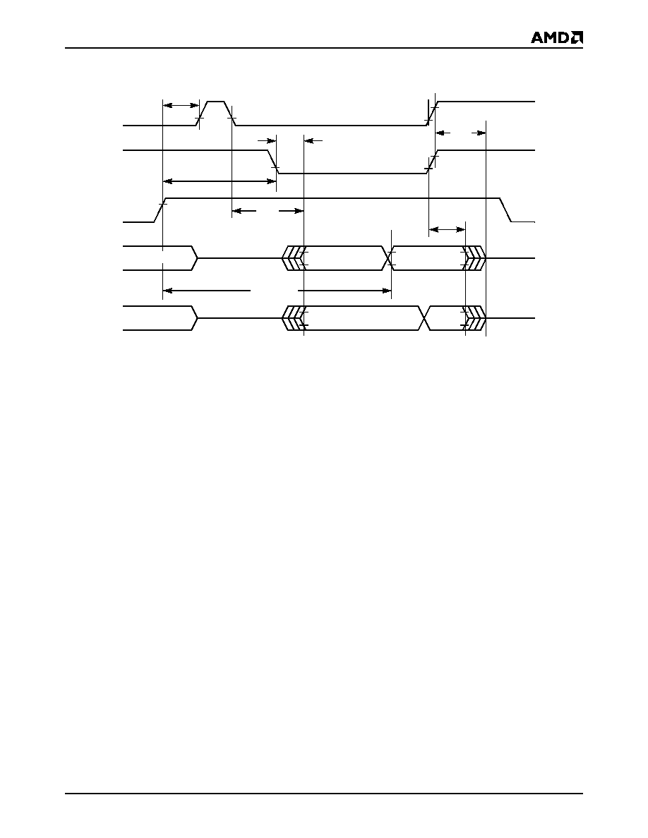
Data Polling--DQ7
The device features Data# Polling as a method to indi-
cate to the host system that the Embedded algorithms
are either in progress or completed.
While the Embedded Programming algorithm is in oper-
ation, an attempt to read the device at a valid address
will produce the complement of expected Valid data on
DQ7. Upon completion of the Embedded Program algo-
rithm an attempt to read the device at a valid address will
produce Valid data on DQ7. The Data# Polling feature is
valid after the rising edge of the second WE# pulse of
the two write pulse sequence.
While the Embedded Erase algorithm is in operation,
DQ7 will read "0" until the erase operation is com-
pleted. Upon completion of the erase operation, the
data on DQ7 will read "1." The Data# Polling feature is
valid after the rising edge of the second WE# pulse of
the two Write pulse sequence.
The Data# Polling feature is only active during Embed-
ded Programming or erase algorithms.
See Figures 3 and 4 for the Data# Polling timing spec-
ifications and diagrams. Data# Polling is the standard
method to check the write operation status, however,
an alternative method is available using Toggle Bit.
START
Fail
No
DQ7 = Data
?
DQ7 = Data
?
DQ5 = 1
?
No
Pass
Yes
No
Yes
Read Byte
(DQ0≠DQ7)
Addr = VA
Read Byte
(DQ0≠DQ7)
Addr = VA
Yes
VA = Byte address for programming
= XXXXh during chip erase
18880C-8
Note:
DQ7 is rechecked even if DQ5 = "1" because DQ7 may change simultaneously with DQ5 or after DQ5.
Figure 3.
Data
#
Polling Algorithm
Am28F512A
15
t
CH
t
OEH
t
OE
t
CE
t
WHWH 3 or 4
DQ7#
DQ7 =
Valid Data
High Z
CE#
OE#
WE#
DQ7
t
OH
t
DF
DQ0≠DQ6 = Invalid
DQ0≠DQ6
DQ0≠DQ7
Valid Data
*
18880C-9
*DQ7 = Valid Data (The device has completed the Embedded operation.)
Figure 4.
AC Waveforms for Data
#
Polling during Embedded Algorithm Operations
16
Am28F512A
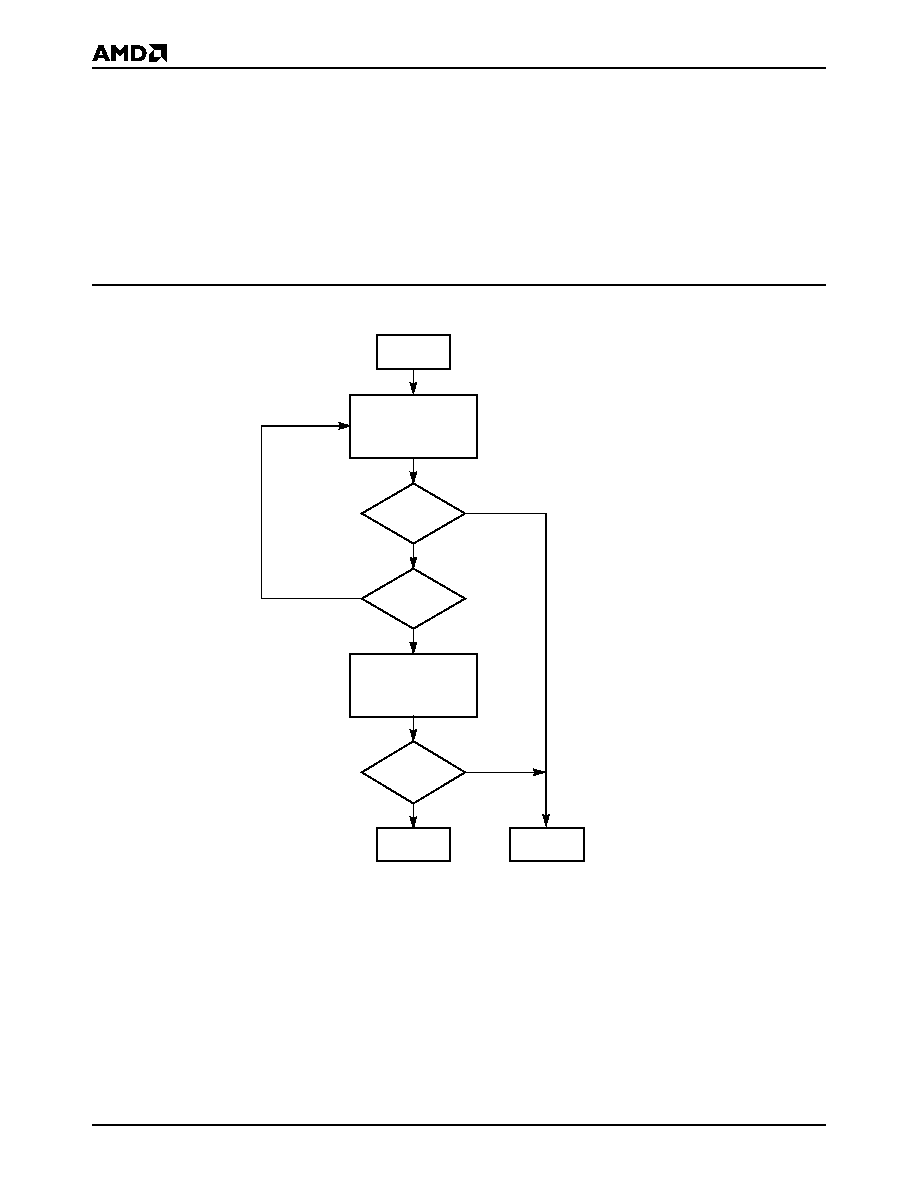
Toggle Bit--DQ6
The device also features a "Toggle Bit" as a method to
indicate to the host system that the Embedded algo-
rithms are either in progress or completed.
Successive attempts to read data from the device at a
valid address, while the Embedded Program algorithm
is in progress, or at any address while the Embedded
Erase algorithm is in progress, will result in DQ6 tog-
gling between one and zero. Once the Embedded Pro-
gram or Erase algorithm is completed, DQ6 will stop
toggling to indicate the completion of either Embedded
operation. Only on the next read cycle will valid data be
obtained. The toggle bit is valid after the rising edge of
the first WE# pulse of the two write pulse sequence, un-
like Data# Polling which is valid after the rising edge of
the second WE# pulse. This feature allows the user to
determine if the device is partially through the two write
pulse sequence.
See Figures 5 and 6 for the Toggle Bit timing specifica-
tions and diagrams.
START
Fail
No
DQ6 = Toggle
?
DQ5 = 1
?
Pass
Yes
No
Read Byte
(DQ0≠DQ7)
Addr = VA
Read Byte
(DQ0≠DQ7)
Addr = VA
Yes
No
Yes
DQ6 = Toggle
?
VA = Byte address for programming
= XXXXh during chip erase
18880C-10
Note:
DQ6 is rechecked even if DQ5 = "1" because DQ6 may stop toggling at the same time as DQ5 changing to "1".
Figure 5.
Toggle Bit Algorithm
Am28F512A
17
DQ5
Exceeded Timing Limits
DQ5 will indicate if the program or erase time has
exceeded the specified limits. This is a failure condi-
tion and the device may not be used again (internal
pulse count exceeded). Under these conditions DQ5
will produce a "1." The program or erase cycle was not
successfully completed. Data# Polling is the only op-
erating function of the device under this condition. The
CE# circuit will partially power down the device under
these conditions (to approximately 2 mA). The OE#
and WE# pins will control the output disable functions
as described in the Command Definitions table in the
corresponding device data sheet.
Parallel Device Erasure
The Embedded Erase algorithm greatly simplifies par-
allel device erasure. Since the erase process is internal
to the device, a single erase command can be given to
multiple devices concurrently. By implementing a paral-
lel erase algorithm, total erase time may be minimized.
Note that the Flash memories may erase at different
rates. If this is the case, when a device is completely
erased, use a masking code to prevent further erasure
(over-erasure). The other devices will continue to erase
until verified. The masking code applied could be the
read command (00h).
Power-Up/Power-Down Sequence
The device powers-up in the Read only mode. Power
supply sequencing is not required. Note that if V
CC
1.0 Volt, the voltage difference between V
PP
and V
CC
should not exceed 10.0 Volts. Also, the device has a
rise V
PP
rise time and fall time specification of 500 ns
minimum.
Reset Command
The Reset command initializes the Flash memory de-
vice to the Read mode. In addition, it also provides the
user with a safe method to abort any device operation
(including program or erase).
The Reset must be written two consecutive times after
the Setup Program command (10h or 50h). This will
reset the device to the Read mode.
Following any other Flash command, write the Reset
command once to the device. This will safely abort any
previous operation and initialize the device to the Read
mode.
The Setup Program command (10h or 50h) is the only
command that requires a two-sequence reset cycle. The
first Reset command is interpreted as program data.
However, FFh data is considered as null data during pro-
gramming operations (memory cells are only pro-
grammed from a logical "1" to "0"). The second Reset
command safely aborts the programming operation and
resets the device to the Read mode.
Memory contents are not altered in any case.
CE#
t
OEH
WE#
OE#
Data
DQ0≠DQ7
DQ6 =
DQ6 =
DQ6
Stop Toggling
DQ0≠DQ7
Valid
t
OE
*
18880C-11
Note:
*DQ6 stops toggling (The device has completed the Embedded operation.)
Figure 6.
AC Waveforms for Toggle Bit during Embedded Algorithm Operations

18
Am28F512A
This detailed information is for your reference. It may
prove easier to always issue the Reset command two
consecutive times. This eliminates the need to deter-
mine if you are in the Setup Program state or not.
In-System Programming Considerations
Flash memories can be programmed in-system or in a
standard PROM programmer. The device may be sol-
dered to the circuit board upon receipt of shipment and
programmed in-system. Alternatively, the device may
initially be programmed in a PROM programmer prior
to soldering the device to the circuit board.
Auto Select Command
AMD's Flash memories are designed for use in appli-
cations where the local CPU alters memory contents.
In order to correctly program any Flash memories
in-system, manufacturer and device codes must be
accessible while the device resides in the target
system. PROM programmers typically access the sig-
nature codes by raising A9 to a high voltage. However,
multiplexing high voltage onto address lines is not a
generally desired system design practice.
The device contains an Auto Select operation to supple-
ment traditional PROM programming methodologies.
The operation is initiated by writing 80h or 90h into the
command register. Following this command, a read
cycle address 0000h retrieves the manufacturer code of
01h (AMD). A read cycle from address 0001h returns
the device code (see the Auto Select Code table of the
corresponding device data sheet). To terminate the op-
eration, it is necessary to write another valid command,
such as Reset (00h or FFh), into the register.

Am28F512A
19
ABSOLUTE MAXIMUM RATINGS
Storage Temperature . . . . . . . . . . . . ≠65
∞
C to +150
∞
C
Plastic Packages . . . . . . . . . . . . . . . ≠65
∞
C to +125
∞
C
Ambient Temperature
with Power Applied. . . . . . . . . . . . . .≠55
∞
C to + 125
∞
C
Voltage with Respect To Ground
All pins except A9 and V
PP
(Note 1) . . . . . . . . . . . . . . . . . . . . . . . ≠2.0 V to +7.0 V
V
CC
(Note 1). . . . . . . . . . . . . . . . . . . . ≠2.0 V to +7.0 V
A9
(Note 2). . . . . . . . . . . . . . . . . . . . ≠2.0 V to +14.0 V
V
PP
(Note 2). . . . . . . . . . . . . . . . . . . ≠2.0 V to +14.0 V
Output Short Circuit Current (Note 3) . . . . . . 200 mA
Notes:
1. Minimum DC voltage on input or I/O pins is ≠0.5 V. During
voltage transitions, inputs may overshoot V
SS
to ≠2.0 V
for periods of up to 20 ns. Maximum DC voltage on input
and I/O pins is V
CC
+ 0.5 V. During voltage transitions,
input and I/O pins may overshoot to V
CC
+ 2.0 V for
periods up to 20 ns.
2. Minimum DC input voltage on A9 and V
PP
pins is ≠0.5 V.
During voltage transitions, A9 and V
PP
may overshoot
V
SS
to ≠2.0 V for periods of up to 20 ns. Maximum DC
input voltage on A9 and V
PP
is +13.0 V which may
overshoot to 14.0 V for periods up to 20 ns.
3. No more than one output shorted to ground at a time.
Duration of the short circuit should not be greater than
one second.
Stresses above those listed under "Absolute Maximum Rat-
ings" may cause permanent damage to the device. This is a
stress rating only; functional operation of the device at these
or any other conditions above those indicated in the opera-
tional sections of this specification is not implied. Exposure of
the device to absolute maximum rating conditions for
extended periods may affect device reliability.
OPERATING RANGES
Commercial (C) Devices
Ambient Temperature (T
A
) . . . . . . . . . . .0
∞
C to +70
∞
C
Industrial (I) Devices
Ambient Temperature (T
A
) . . . . . . . . .≠40
∞
C to +85
∞
C
Extended (E) Devices
Ambient Temperature (T
A
) . . . . . . . .≠55
∞
C to +125
∞
C
V
CC
Supply Voltages
V
CC
. . . . . . . . . . . . . . . . . . . . . . . +4.50 V to +5.50 V
V
PP
Voltages
Read . . . . . . . . . . . . . . . . . . . . . . . . ≠0.5 V to +12.6 V
Program, Erase, and Verify . . . . . . +11.4 V to +12.6 V
Operating ranges define those limits between which the
functionality of the device is guaranteed.
20
Am28F512A
MAXIMUM OVERSHOOT
20 ns
20 ns
+0.8 V
≠0.5 V
20 ns
≠2.0 V
18880C-12
Maximum Negative Input Overshoot
20 ns
V
CC
+ 0.5 V
2.0 V
20 ns
20 ns
V
CC
+ 2.0 V
18880C-13
Maximum Positive Input Overshoot
18880C-14
Maximum V
PP
Overshoot
20 ns
13.5 V
V
CC
+ 0.5 V
20 ns
20 ns
14.0 V
Am28F512A
21
DC CHARACTERISTICS over operating range unless otherwise specified
TTL/NMOS Compatible
Notes:
1. Caution: The Am28F512A must not be removed from (or inserted into) a socket when V
CC
or V
PP
is applied. If V
CC
1.0
volt, the voltage difference between V
PP
and V
CC
should not exceed 10.0 volts. Also, the Am28F512A has a V
PP
rise time
and fall time specification of 500 ns minimum.
2. I
CC1
is tested with OE
#
= V
IH
to simulate open outputs.
3. Maximum active power usage is the sum of I
CC
and I
PP
.
4. Not 100% tested.
Parameter
Symbol
Parameter Description
Test Conditions
Min
Typ
Max
Unit
I
LI
Input Leakage Current
V
CC
= V
CC
Max, V
IN
= V
CC
or V
SS
±
1.0
µA
I
LO
Output Leakage Current
V
CC
= V
CC
Max, V
OUT
= V
CC
or V
SS
±
1.0
µA
I
CCS
V
CC
Standby Current
V
CC
= V
CC
Max, CE
#
= V
IH
0.2
1.0
mA
I
CC1
V
CC
Active Read Current
V
CC =
V
CC
Max, CE
#
= V
IL,
OE
#
= V
IH
I
OUT
= 0 mA, at 6 MHz
20
30
mA
I
CC2
V
CC
Programming Current
CE
#
=
V
IL
Programming in Progress (Note 4)
20
30
mA
I
CC3
V
CC
Erase Current
CE
#
=
V
IL
Erasure in Progress (Note 4)
20
30
mA
I
PPS
V
PP
Standby Current
V
PP
= V
PPL
±
1.0
µA
I
PP1
V
PP
Read Current
V
PP
= V
PPH
70
200
µA
V
PP
= V
PPL
±
1.0
I
PP2
V
PP
Programming Current
V
PP
= V
PPH
Programming in Progress (Note 4)
10
30
mA
I
PP3
V
PP
Erase Current
V
PP
= V
PPH
Erasure in Progress (Note 4)
10
30
mA
V
IL
Input Low Voltage
≠0.5
0.8
V
V
IH
Input High Voltage
2.0
V
CC
+ 0.5
V
V
OL
Output Low Voltage
I
OL
= 5.8 mA, V
CC
= V
CC
Min
0.45
V
V
OH1
Output High Voltage
I
OH
= ≠2.5 mA, V
CC
= V
CC
Min
2.4
V
V
ID
A9 Auto Select Voltage
A9 = V
ID
11.5
13.0
V
I
ID
A9 Auto Select Current
A9 = V
ID
Max, V
CC
= V
CC
Max
5
50
µA
V
PPL
V
PP
during Read-Only
Operations
Note: Erase/Program are inhibited
when V
PP
= V
PPL
0.0
V
CC
+2.0
V
V
PPH
V
PP
during Read/Write
Operations
11.4
12.6
V
V
LKO
Low V
CC
Lock-out Voltage
3.2
3.7
V
22
Am28F512A
DC CHARACTERISTICS
CMOS Compatible
Notes:
1. Caution: The Am28F512A must not be removed from (or inserted into) a socket when V
CC
or V
PP
is applied. If V
CC
1.0 volt,
the voltage difference between V
PP
and V
CC
should not exceed 10.0 volts. Also, the Am28F512A has a V
PP
rise time and fall
time specification of 500 ns minimum.
2. I
CC1
is tested with OE
#
= V
IH
to simulate open outputs.
3. Maximum active power usage is the sum of I
CC
and I
PP
.
4. Not 100% tested.
Parameter
Symbol
Parameter Description
Test Conditions
Min
Typ
Max
Unit
I
LI
Input Leakage Current
V
CC
= V
CC
Max, V
IN
= V
CC
or V
SS
±
1.0
µA
I
LO
Output Leakage Current
V
CC
= V
CC
Max, V
OUT
= V
CC
or V
SS
±
1.0
µA
I
CCS
V
CC
Standby Current
V
CC
= V
CC
Max, CE
#
= V
CC
+ 0.5 V
15
100
µA
I
CC1
V
CC
Active Read Current
V
CC
= V
CC
Max, CE
#
= V
IL,
OE
#
= V
IH
I
OUT
= 0 mA, at 6 MHz
20
30
mA
I
CC2
V
CC
Programming Current
CE
#
= V
IL
Programming in Progress (Note 4)
20
30
mA
I
CC3
V
CC
Erase Current
CE
#
= V
IL
Erasure in Progress (Note 4)
20
30
mA
I
PPS
V
PP
Standby Current
V
PP
= V
PPL
±
1.0
µA
I
PP1
V
PP
Read Current
V
PP
= V
PPH
70
200
µA
I
PP2
V
PP
Programming Current
V
PP
= V
PPH
Programming in Progress (Note 4)
10
30
mA
I
PP3
V
PP
Erase Current
V
PP
= V
PPH
Erasure in Progress (Note 4)
10
30
mA
V
IL
Input Low Voltage
≠0.5
0.8
V
V
IH
Input High Voltage
0.7 V
CC
V
CC
+ 0.5
V
V
OL
Output Low Voltage
I
OL
= 5.8 mA, V
CC
= V
CC
Min
0.45
V
V
OH1
Output High Voltage
I
OH
= ≠2.5 mA, V
CC
= V
CC
Min
0.85 V
CC
V
V
OH2
I
OH
= ≠100 µA, V
CC
= V
CC
Min
V
CC
≠0.4
V
ID
A9 Auto Select Voltage
A9 = V
ID
11.5
13.0
V
I
ID
A9 Auto Select Current
A9 = V
ID
Max, V
CC
= V
CC
Max
5
50
µA
V
PPL
V
PPL
during Read-Only
Operations
Note: Erase/Program are inhibited
when V
PP
= V
PPL
0.0
V
CC
+ 2.0
V
V
PPH
V
PP
during Read/Write
Operations
11.4
12.6
V
V
LKO
Low V
CC
Lock-out Voltage
3.2
3.7
V
23
Am28F512A
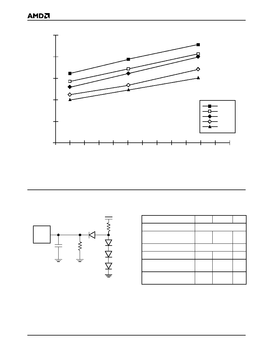
Figure 7.
Am28F512A--Average I
CC
Active vs. Frequency
V
CC
= 5.5 V, Addressing Pattern = Minmax
Data Pattern = Checkerboard
TEST CONDITIONS
Table 6.
Test Specifications
I
CC
Act
ive
in
mA
25
20
15
10
5
0
0
1
2
3
4
5
6
7
8
9
10
11
12
Frequency in MHz
55
∞
C
0
∞
C
25
∞
C
70
∞
C
125
∞
C
18880B-15
2.7 k
CL
6.2 k
5.0 V
Device
Under
Test
18880C-16
Figure 8.
Test Setup
Note: Diodes are IN3064 or equivalent
Test Condition
-70
All others
Unit
Output Load
1 TTL gate
Output Load Capacitance, C
L
(including jig capacitance)
30
100 pF
Input Rise and Fall Times
10
ns
Input Pulse Levels
0.0≠3.0
0.45≠2.4
V
Input timing measurement
reference levels
1.5
0.8, 2.0
V
Output timing measurement
reference levels
1.5
0.8, 2.0
V
Am28F512A
24
SWITCHING TEST WAVEFORMS
SWITCHING CHARACTERISTICS over operating range unless otherwise specified
AC Characteristics--Read Only Operation
Notes:
1. Guaranteed by design not tested.
2. Not 100% tested.
Parameter Symbols
Parameter Description
Am28F512A Speed Options
Unit
JEDEC
Standard
-70
-90
-120
-150
-200
t
AVAV
t
RC
Read Cycle Time (Note 2)
Min
70
90
120
150
200
ns
t
ELQV
t
CE
Chip Enable Access Time
Max
70
90
120
150
200
ns
t
AVQV
t
ACC
Address Access Time
Max
70
90
120
150
200
ns
t
GLQV
t
OE
Output Enable Access Time
Max
35
35
50
55
55
ns
t
ELQX
t
LZ
Chip Enable to Output in Low Z
(Note 2)
Min
0
0
0
0
0
ns
t
EHQZ
t
DF
Chip Disable to Output in High Z
(Note 1)
Max
20
20
30
35
35
ns
t
GLQX
t
OLZ
Output Enable to Output in Low Z
(Note 2)
Min
0
0
0
0
0
ns
t
GHQZ
t
DF
Output Disable to Output in
High Z (Note 2)
Max
20
20
30
35
35
ns
t
AXQX
t
OH
Output Hold from first of Address,
CE
#
, or OE
#
Change (Note 2)
Min
0
0
0
0
0
ns
t
VCS
V
CC
Setup Time to Valid Read
(Note 2)
Min
50
50
50
50
50
µs
18880C-17
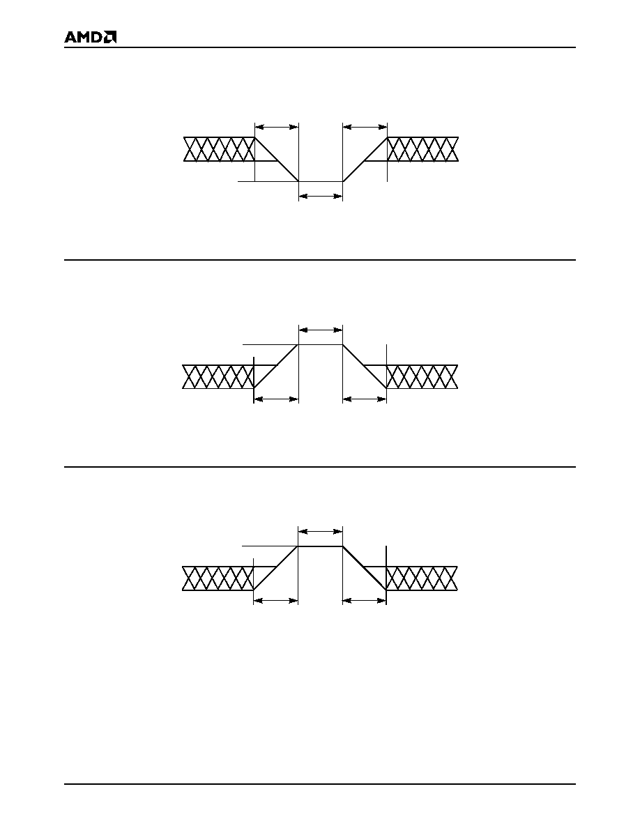
3 V
0 V
Input
Output
1.5 V
1.5 V
Test Points
AC Testing for -70 devices: Inputs are driven at 3.0 V for a
logic "1" and 0 V for a logic "0". Input pulse rise and fall times
are
10 ns.
2.4 V
0.45 V
Input
Output
Test Points
2.0 V
2.0 V
0.8 V
0.8 V
AC Testing (all speed options except -70): Inputs are driven
at 2.4 V for a logic "1" and 0.45 V for a logic "0". Input pulse
rise and fall times are
10 ns.
25
Am28F512A
AC Characteristics--Write/Erase/Program Operations
Notes:
1. Read timing characteristics during read/write operations are the same as during read-only operations. Refer to AC
Characteristics for Read Only operations.
2. Embedded Program Operation of 14 µs consists of 10 µs program pulse and 4 ms write recovery before read. This is the
minimum time for one pass through the programming algorithm.
3. Embedded Erase Operation of 5 sec consists of 4 sec array pre-programming time and one sec array erase time. This is a
typical time for one embedded erase operation.
4. Not 100% tested.
Parameter Symbols
Parameter Description
Am28F512A Speed Options
Unit
JEDEC
Standard
-70
-90
-120
-150
-200
t
AVAV
t
WC
Write Cycle Time (Note 4)
Min
70
90
120
150
200
ns
t
AVWL
t
AS
Address Setup Time
Min
0
0
0
0
0
ns
t
WLAX
t
AH
Address Hold Time
Min
45
45
50
60
75
ns
t
DVWH
t
DS
Data Setup Time
Min
45
45
50
50
50
ns
t
WHDX
t
DH
Data Hold Time
Min
10
10
10
10
10
ns
t
OEH
Output Enable Hold Time
for Embedded Algorithm only
Min
10
10
10
10
10
µs
t
GHWL
Read Recovery Time before Write
Min
0
0
0
0
0
µs
t
ELWLE
t
CSE
Chip Enable Embedded Algorithm
Setup Time
Min
20
20
20
20
20
ns
t
WHEH
t
CH
Chip Enable Hold Time
Min
0
0
0
0
0
ns
t
WLWH
t
WP
Write Pulse Width
Min
45
45
50
60
60
ns
t
WHWL
t
WPH
Write Pulse Width HIGH
Min
20
20
20
20
20
ns
t
WHWH3
Embedded Programming Operation
(Note 2)
Min
14
14
14
14
14
µs
t
WHWH4
Embedded Erase Operation (Note 2)
Typ
5
5
5
5
5
ms
t
VPEL
V
PP
Setup Time to Chip Enable LOW
(Note 4)
Min
100
100
100
100
100
ns
t
VCS
V
CC
Setup Time to Chip Enable LOW
(Note 4)
Min
50
50
50
50
50
µs
t
VPPR
V
PP
Rise Time 90% V
PPH
(Note 4)
Min
500
500
500
500
500
ns
t
VPPF
V
PP
Fall Time 10% V
PPL
(Note 4)
Min
500
500
500
500
500
ns
t
LKO
V
CC
< V
LKO
to Reset (Note 4)
Min
100
100
100
100
100
ns
Am28F512A
26
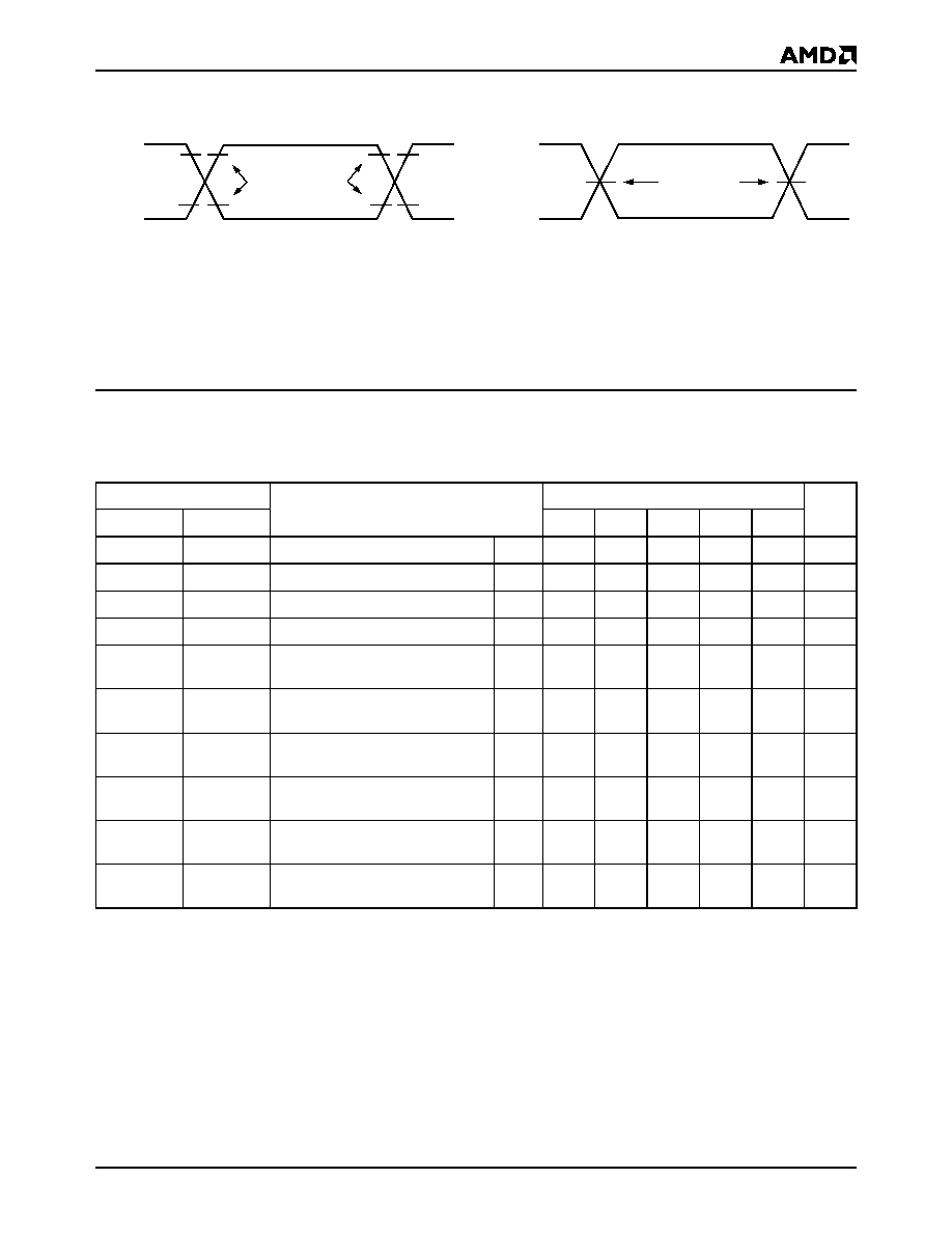
KEY TO SWITCHING WAVEFORMS
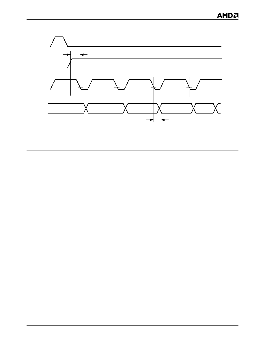
SWITCHING WAVEFORMS
WAVEFORM
INPUTS
OUTPUTS
Steady
Changing from H to L
Changing from L to H
Don't Care, Any Change Permitted
Changing, State Unknown
Does Not Apply
Center Line is High Impedance State (High Z)
Addresses
CE
#
(E
#
)
OE
#
(G
#
)
WE
#
(W
#
)
Data (DQ)
5.0 V
V
CC
0 V
Power-up, Standby
Device and
Address Selection
Outputs
Enabled
Data
Valid
Standby, Power-down
Addresses Stable
High Z
High Z
t
WHGL
t
AVQV
(t
ACC
)
t
EHQZ
(t
DF
)
t
GHQZ
(t
DF
)
t
ELQX
(t
LZ
)
t
GLQX
(t
OLZ
)
t
ELQV
(t
CE
)
t
GLQV
(t
OE
)
t
AXQX
(t
OH
)
Output Valid
t
AVAV
(t
RC
)
t
VCS
18880C-18
Figure 9.
AC Waveforms for Read Operations
27
Am28F512A
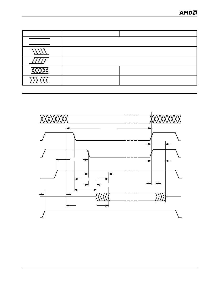
SWITCHING WAVEFORMS
t
WC
DQ7#
30h
t
RC
Data
#
Polling
Read
t
DF
t
OH
t
CE
t
OE
t
DS
t
CSE
t
WPH
t
DH
t
WP
t
GHWL
t
WHWH3 OR 4
Addresses
CE
#
OE
#
WE
#
Data
V
CC
V
PP
Embedded
Erase Setup
Embedded
Erase
Erase
Standby
30h
t
AH
t
AS
t
VCS
t
VPEL
DQ7#
18880C-19
Note:
DQ7
#
is the complement of the data written to the device.
Figure 10.
AC Waveforms for Embedded Erase Operation
Am28F512A
28
SWITCHING WAVEFORMS
t
WC
t
DS
DQ7
#
D
IN
t
AS
t
AH
t
RC
Data
#
Polling
Read
t
DF
t
OH
t
CE
t
OE
t
WPH
t
DH
t
WP
t
GHWL
Embedded
Program Setup
Embedded
Program
t
CSE
t
WHWH3 OR 4
50h
PA
t
VCS
t
VPEL
PA
DQ7#
DOUT
18880C-20
Notes:
1. D
IN
is data input to the device.
2. DQ7
#
is the complement of the data written to the device.
3. D
OUT
is the data written to the device.
Figure 11.
AC Waveforms for Embedded Programming Operation
Addresses
CE
#
OE
#
WE
#
Data
V
CC
V
PP
29
Am28F512A
AC CHARACTERISTICS--WRITE/ERASE/PROGRAM OPERATIONS
Alternate CE
#
Controlled Writes
Notes:
1. Read timing characteristics during read/write operations are the same as during read-only operations. Refer to AC
Characteristics for Read Only operations.
2. Embedded Program Operation of 14 µs consists of 10 µs program pulse and 4 ms write recovery before read. This is the
minimum time for one pass through the programming algorithm.
3. Embedded Erase Operation of 5 sec consists of 4 sec array pre-programming time and one sec array erase time. This is a
typical time for one embedded erase operation.
4. Not 100% tested.
Parameter Symbols
Parameter Description
Am28F512A Speed Options
Unit
JEDEC
Standard
-70
-90
-120
-150
-200
t
AVAV
t
WC
Write Cycle Time (Note 4)
Min
70
90
120
150
200
ns
t
AVEL
t
AS
Address Setup Time
Min
0
0
0
0
0
ns
t
ELAX
t
AH
Address Hold Time
Min
45
45
50
60
75
ns
t
DVEH
t
DS
Data Setup Time
Min
45
45
50
50
50
ns
t
EHDX
t
DH
Data Hold Time
Min
10
10
10
10
10
ns
t
OEH
Output Enable Hold Time
for Embedded Algorithm only
Min
10
10
10
10
10
µs
t
GHEL
Read Recovery Time before Write
Min
0
0
0
0
0
ns
t
WLEL
t
WS
WE# Setup Time by CE
#
Min
0
0
0
0
0
ns
t
EHWK
t
WH
WE# Hold Time
Min
0
0
0
0
0
ns
t
ELEH
t
CP
Write Pulse Width
Min
65
65
70
80
80
ns
t
EHEL
t
CPH
Write Pulse Width HIGH
Min
20
20
20
20
20
ns
t
EHEH3
Embedded Programming Operation
(Note 2)
Min
14
14
14
14
14
µs
t
EHEH4
Embedded Erase Operation (Note 3)
Typ
5
5
5
5
5
sec
t
VPEL
V
PP
Setup Time to Chip Enable LOW
(Note 4)
Min
100
100
100
100
100
ns
t
VCS
V
CC
Setup Time to Chip Enable LOW
(Note 4)
Min
50
50
50
50
50
µs
t
VPPR
V
PP
Rise Time 90% V
PPH
(Note 4)
Min
500
500
500
500
500
ns
t
VPPF
V
PP
Fall Time 10% V
PPL
(Note 4)
Min
500
500
500
500
500
ns
t
LKO
V
CC
< V
LKO
to Reset (Note 4)
Min
100
100
100
100
100
ns
Am28F512A
30
SWITCHING WAVEFORMS
t
VPEL
t
WC
Data
#
Polling
PA
DQ7
#
D
IN
t
AS
t
AH
t
GHEL
t
DH
t
CPH
t
EHEH3 OR 4
t
WS
t
DS
t
CP
Embedded
Program Setup
Embedded
Program
PA
D
OUT
DQ7
#
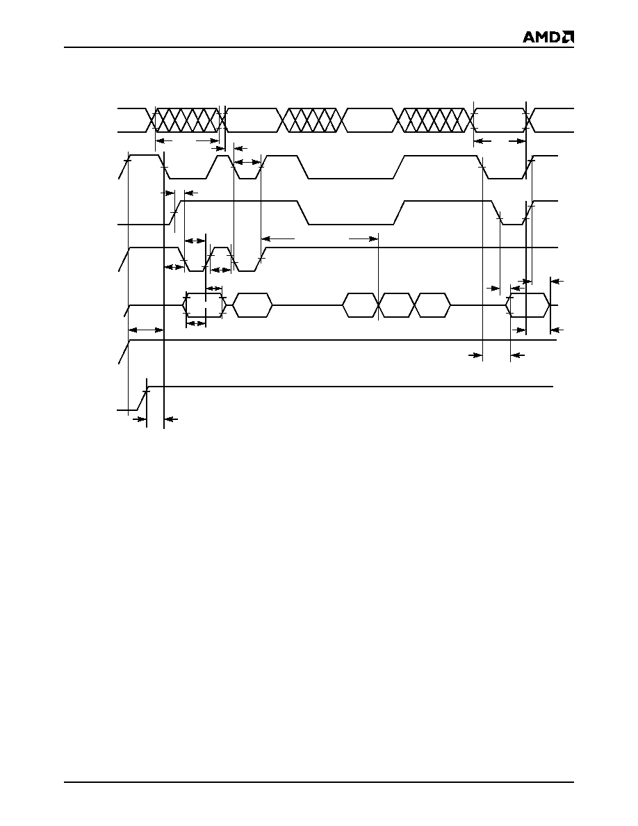
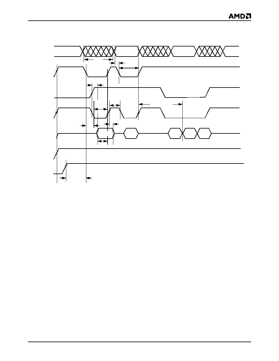
18880C-21
Notes:
1. D
IN
is data input to the device.
2. DQ7
#
is the complement of the data written to the device.
3. D
OUT
is the data written to the device.
Figure 12.
AC Waveforms for Embedded Programming Operation Using CE# Controlled Writes
Addresses
CE
#
OE
#
WE#
Data
V
CC
V
PP
50h
31
Am28F512A
ERASE AND PROGRAMMING PERFORMANCE
Notes:
1. 25
∞
C, 12 V V
PP
.
2. Maximum time specified is lower than worst case. Worst case is derived from the Embedded Algorithm internal counter which
allows for a maximum 6000 pulses for both program and erase operations. Typical worst case for program and erase is
significantly less than the actual device limit.
3. Typical worst case = 84 µs. DQ5 = "1" only after a byte takes longer than 96 ms to program.
LATCHUP CHARACTERISTICS
PIN CAPACITANCE
Note: Sampled, not 100% tested. Test conditions T
A
= 25∞C, f = 1.0 MHz.
DATA RETENTION
Parameter
Limits
Comments
Min
Typ
(Note 1)
Max
(Note 2)
Unit
Chip Erase Time
1
10
sec
Excludes 00h programming prior to erasure
Chip Programming Time
1
7
sec
Excludes system-level overhead
Write/Erase Cycles
100,000
Cycles
Byte Programming Time
14
µs
96
(Note 3)
ms
Parameter
Min
Max
Input Voltage with respect to V
SS
on all pins except I/O pins (Including A9 and V
PP
)
≠1.0 V
13.5 V
Input Voltage with respect to V
SS
on all pins I/O pins
≠1.0 V
V
CC
+ 1.0 V
Current
≠100 mA
+100 mA
Includes all pins except V
CC
. Test conditions: V
CC
= 5.0 V, one pin at a time.
Parameter
Symbol
Parameter Description
Test Conditions
Typ
Max
Unit
C
IN
Input Capacitance
V
IN
= 0
8
10
pF
C
OUT
Output Capacitance
V
OUT
= 0
8
12
pF
C
IN2
V
PP
Input Capacitance
V
PP
= 0
8
12
pF
Parameter
Test Conditions
Min
Unit
Minimum Pattern Data Retention Time
150
∞
C
10
Years
125
∞
C
20
Years
Am28F512A
32
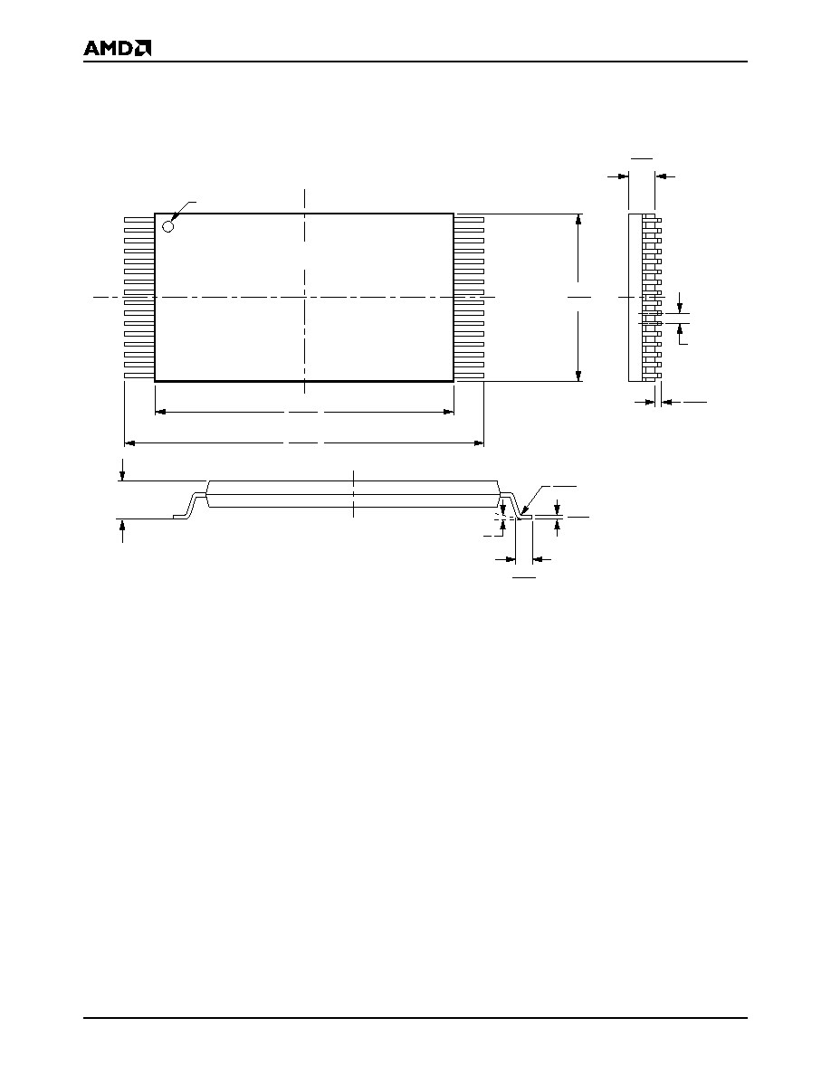
PHYSICAL DIMENSIONS
PD032--32-Pin Plastic DIP (measured in inches)
PL032--32-Pin Plastic Leaded Chip Carrier (measured in inches)
Pin 1 I.D.
1.640
1.670
.530
.580
.005 MIN
.045
.065
.090
.110
.140
.225
.120
.160
.016
.022
SEATING PLANE
.015
.060
16-038-S_AG
PD 032
EC75
5-28-97 lv
32
17
16
.630
.700
0
∞
10
∞
.600
.625
.009
.015
.050 REF.
.026
.032
TOP VIEW
Pin 1 I.D.
.485
.495
.447
.453
.585
.595
.547
.553
16-038FPO-5
PL 032
DA79
6-28-94 ae
SIDE VIEW
SEATING
PLANE
.125
.140
.009
.015
.080
.095
.042
.056
.013
.021
.400
REF.
.490
.530
33
Am28F512A
PHYSICAL DIMENSIONS
TS032--32-Pin Standard Thin Small Outline Package (measured in millimeters)
Pin 1 I.D.
1
18.30
18.50
7.90
8.10
0.50 BSC
0.05
0.15
0.95
1.05
16-038-TSOP-2
TS 032
DA95
3-25-97 lv
19.80
20.20
1.20
MAX
0.50
0.70
0.10
0.21
0
∞
5
∞
0.08
0.20
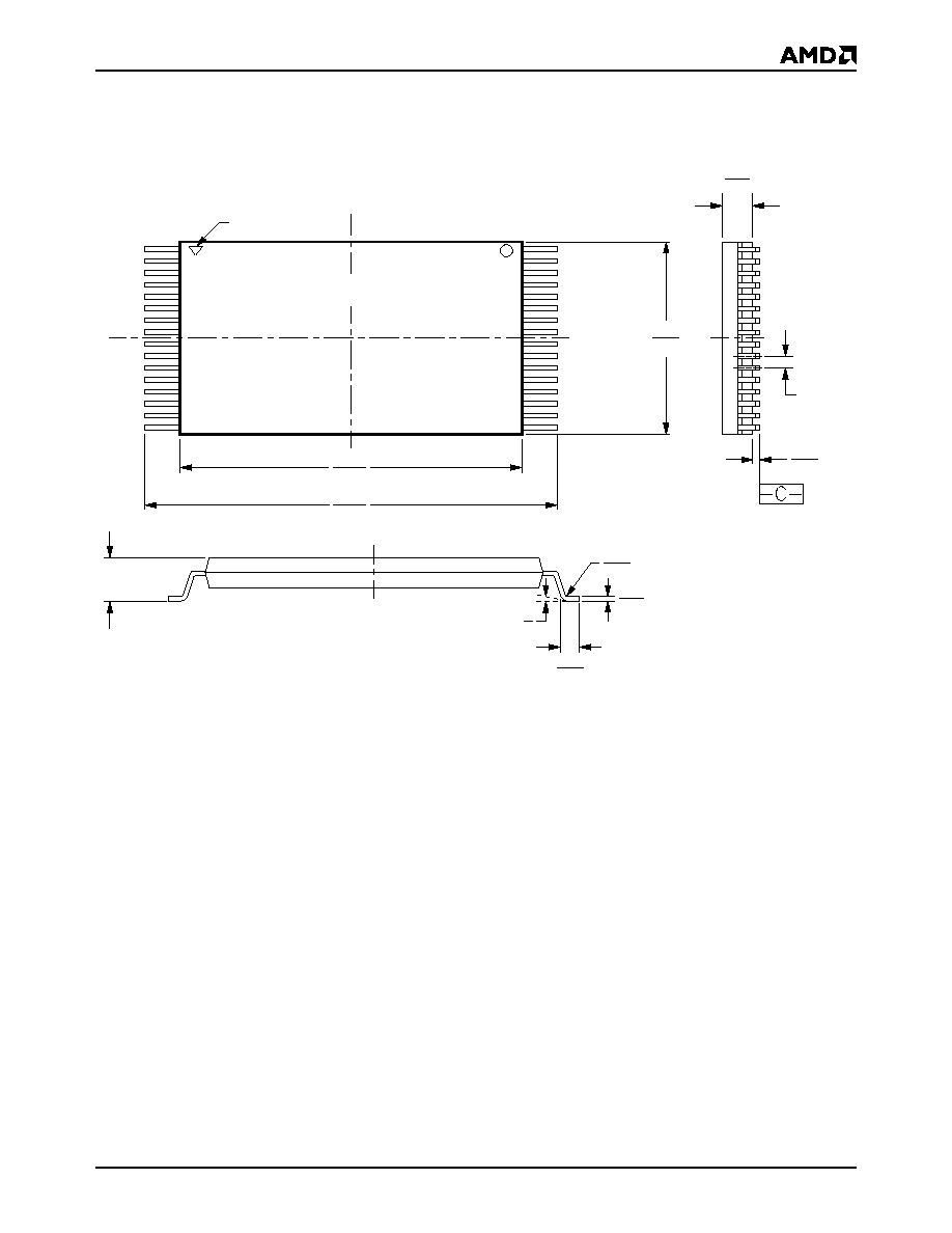
Am28F512A
34
PHYSICAL DIMENSIONS
TSR032--32-Pin Reversed Thin Small Outline Package (measured in millimeters)
DATA SHEET REVISION SUMMARY FOR AM28F512A
Revision C
Deleted -75, -95, and -250 speed options. Matched for-
matting to other current data sheets.
Revision C+1
Programming In A PROM Programmer
Deleted the paragraph "(Refer to the AUTO SELECT
paragraph in the ERASE, PROGRAM, and READ
MODE section for programming the Flash memory de-
vice in-system)."
Revision C+2
Product Selector Guide
Corrected maximum access time for -200 to 200 ns.
Connection Diagrams
On standard TSOP, corrected pin 9 to V
PP
and pin 10
to NC. On reverse TSOP, corrected pin 23 to NC and
pin 24 to V
PP
.
Trademarks
Copyright © 1998 Advanced Micro Devices, Inc. All rights reserved.
ExpressFlash is a trademark of Advanced Micro Devices, Inc.
AMD, the AMD logo, and combinations thereof are registered trademarks of Advanced Micro Devices, Inc.
Product names used in this publication are for identification purposes only and may be trademarks of their respective companies.
1
18.30
18.50
19.80
20.20
7.90
8.10
0.50 BSC
0.05
0.15
0.95
1.05
16-038-TSOP-2
TSR032
DA95
3-25-97 lv
Pin 1 I.D.
1.20
MAX
0.50
0.70
0.10
0.21
0
∞
5
∞
0.08
0.20